

Linear Technology LTC1655L Datasheet
1
LTC1655L
16-Bit Rail-to-Rail
Micropower DAC in
SO-8 Package
August 1999
FEATURES
■
16-Bit Monotonicity Over Temperature
■
3V Single Supply Operation
■
Deglitched Rail-to-Rail Voltage Output
■
SO-8 Package
■
I
CC(TYP)
: 600µA
■
Internal 1.25V Reference or External
Reference Override
■
Maximum DNL Error: 1LSB
■
Power-On Reset
■
3-Wire Cascadable Serial Interface
■
Low Cost
■
Pin Compatible Upgrade to 12-Bit LTC1453
■
5V Version Available (LTC1655)
The LTC®1655L is a rail-to-rail voltage output, 16-bit
digital-to-analog converter (DAC) in an SO-8 package. It
includes an output buffer and a reference. The 3-wire serial
interface is compatible with SPI/QSPI and MICROWIRE
TM
protocols. The SCK input has a Schmitt trigger that allows
direct optocoupler interface.
The LTC1655L has an onboard 1.25V reference that can be
overdriven to a higher voltage. The output swings from 0V
to 2.5V when using the internal reference. The typical
power dissipation is 1.6mW on a single 3V supply.
The LTC1655L is pin compatible with Linear Technology’s
12-bit V
OUT
DAC family, allowing an easy upgrade path.
It is the only buffered 16-bit DAC in an SO-8 package and
it includes an onboard reference for stand alone
performance.
DESCRIPTION
U
■
Digital Calibration
■
Industrial Process Control
■
Automatic Test Equipment
■
Smart Remote Transmitters
APPLICATIONS
U
, LTC and LT are registered trademarks of Linear Technology Corporation.
MICROWIRE is a trademark of National Semiconductor Corporation.
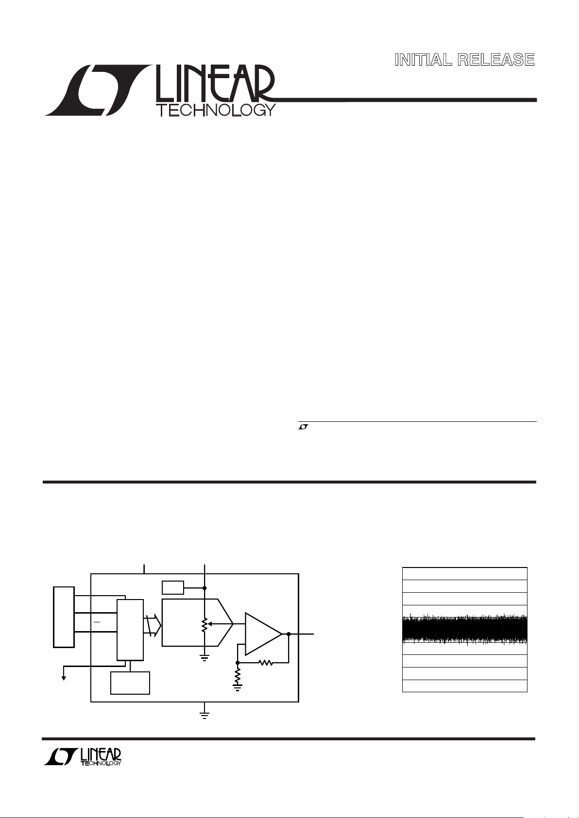
–
+
16-BIT
DAC
2.7V TO 5.5V 1.25V
GND
R
R
POWER-ON
RESET
TO
OTHER
DACS
16-BIT
SHIFT
REG
AND
DAC
LATCH
µP
D
IN
V
CC
16
REF
2
86
D
OUT
4
5
1655 TA01
SCK1
CS/LD3
7
RAIL-TO-RAIL
VOLTAGE
OUTPUT
(0V TO 2.5V)
V
OUT
REF
A 16-Bit Rail-to-Rail V
OUT
DAC Differential Nonlinearity
vs Input Code
CODE
0
–1.0
–0.2
–0.4
–0.6
–0.8
0
0.2
0.4
0.6
0.8
1.0
DNL ERROR (LSB)
16384 32768
1655 TA02
49152
65535
Final Electrical Specifications
Information furnished by Linear Technology Corporation is believed to be accurate and reliable.
However, no responsibility is assumed for its use. Linear Technology Corporation makes no representation that the interconnection of its circuits as described herein will not infringe on existing patent rights.
BLOCK DIAGRA
W
2
LTC1655L
ABSOLUTE MAXIMUM RATINGS
W
WW
U
ORDER PART
NUMBER
WU
U
PACKAGE
/
O
RDER I FOR ATIO
LTC1655LCN8
LTC1655LIN8
LTC1655LCS8
LTC1655LIS8
S8 PART MARKING
1655L
1655LI
Consult factory for Military grade parts.
SYMBOL PARAMETER CONDITIONS MIN TYP MAX UNITS
DAC
Resolution ● 16 Bits
Monotonicity ● 16 Bits
DNL Differential Nonlinearity Guaranteed Monotonic (Note 2) ● ±0.3 ±1.0 LSB
INL Integral Nonlinearity REF = 1.3V (External) (Note 2) ● ±8 ±20 LSB
ZSE Zero-Scale Error ● 0 3.5 mV
V
OS
Offset Error Measured at Code 200 ● ±0.5 ±3.5 mV
VOSTC Offset Error Tempco ±5 µV/°C
Gain Error REF = 2.2V (External) ● ±5 ±16 LSB
Gain Error Drift 0.5 ppm/°C
Power Supply
V
CC
Positive Supply Voltage For Specified Performance ● 2.7 5.5 V
I
CC
Supply Current 2.7V ≤ VCC ≤ 5.5V (Note 4) ● 600 1200 µA
Op Amp DC Performance
Short-Circuit Current Low V
OUT
Shorted to GND ● 70 140 mA
Short-Circuit Current High V
OUT
Shorted to V
CC
● 80 150 mA
Output Impedance to GND Input Code = 0 ● 80 160 Ω
Output Line Regulation Input Code = 65535, VCC = 2.7V to 5.5V, ● ±3 mV/V
with Internal Reference
AC Performance
Voltage Output Slew Rate (Note 3) ● ±0.3 ±0.7 V/µs
Voltage Output Settling Time (Note 3) to 0.0015% (16-Bit Settling Time) 20 µs
(Note 3) to 0.012% (13-Bit Settling Time) 10 µs
Digital Feedthrough 0.3 nV •s
Midscale Glitch Impulse DAC Switched Between 8000 and 7FFF 12 nV•s
(Note 1)
VCC to GND .............................................. –0.5V to 7.5V
TTL Input Voltage .................................... –0.5V to 7.5V
V
OUT
, REF ....................................... –0.5V to V
CC
+ 0.5V
Maximum Junction Temperature ......................... 125°C
Operating Temperature Range
LTC1655LC ............................................ 0°C to 70°C
LTC1655LI......................................... –40°C to 85°C
Storage Temperature Range ................ –65°C to 150°C
Lead Temperature (Soldering, 10 sec)................. 300°C
1
2
3
4
8
7
6
5
TOP VIEW
V
CC
V
OUT
REF
GND
SCK
D
IN
CS/LD
D
OUT
S8 PACKAGE
8-LEAD PLASTIC SO
N8 PACKAGE
8-LEAD PDIP
T
JMAX
= 125°C, θJA = 100°C/W (N8)
T
JMAX
= 125°C, θJA = 150°C/W (S8)
The ● denotes specifications which apply over the full operating temperature range, otherwise specifications are at TA = 25°C.
VCC = 2.7V to 5.5V, V
OUT
unloaded, REF unloaded.
ELECTRICAL CHARACTERISTICS
3
LTC1655L
ELECTRICAL CHARACTERISTICS
SYMBOL PARAMETER CONDITIONS MIN TYP MAX UNITS
Digital I/O
V
IH
Digital Input High Voltage VCC = 3V ● 2V
V
IL
Digital Input Low Voltage VCC = 3V ● 0.6 V
V
OH
Digital Output High Voltage I
OUT
= –1mA, D
OUT
Only, VCC = 3V ● VCC – 0.7 V
V
OL
Digital Output Low Voltage I
OUT
= 1mA, D
OUT
Only, VCC = 3V ● 0.4 V
I
LEAK
Digital Input Leakage VIN = GND to VCC, VCC = 3V ● ±10 µA
C
IN
Digital Input Capacitance (Note 6) 10 pF
Timing Characteristics
t
1
DIN Valid to SCK Setup VCC = 3V ● 60 ns
t
2
DIN Valid to SCK Hold VCC = 3V ● 0ns
t
3
SCK High Time VCC = 3V (Note 6) ● 60 ns
t
4
SCK Low Time VCC = 3V (Note 6) ● 60 ns
t
5
CS/LD Pulse Width VCC = 3V (Note 6) ● 80 ns
t
6
LSB SCK to CS/LD VCC = 3V (Note 6) ● 60 ns
t
7
CS/LD Low to SCK VCC = 3V (Note 6) ● 30 ns
t
8
D
OUT
Output Delay VCC = 3V, C
LOAD
= 100pF ● 20 300 ns
t
9
SCK Low to CS/LD Low VCC = 3V (Note 6) ● 30 ns
Reference Output
Reference Output Voltage ● 1.24 1.25 1.26 V
Reference Input Range (Notes 5, 6) 1.3 VCC/2 V
Reference Output Tempco 5 ppm/°C
Reference Input Resistance REF Overdriven to 1.3V ● 713 kΩ
Reference Short-Circuit Current ● 40 100 mA
Reference Output Line Regulation VCC = 2.7V to 5.5V ● ±1.5 mV/V
Reference Load Regulation I
OUT
= 100µA ● 0.5 mV
Note 1: Absolute Maximum Ratings are those values beyond which the life
of a device may be impaired.
Note 2: Nonlinearity is defined from code 128 to code 65535 (full scale).
See Applications Information.
Note 3: DAC switched between all 1s and code 400, slew rate is measured
from 0.75V to 1.75V.
Note 4: Digital inputs at 0V or V
CC
.
Note 5: Reference can be overdriven (see Applications Information).
Note 6: Guaranteed by design. Not subject to test.
The ● denotes specifications which apply over the full operating temperature range, otherwise specifications are at TA = 25°C.
VCC = 2.7V to 5.5V, V
OUT
unloaded, REF unloaded.
 Loading...