

Linear Technology LTC1654 Datasheet
LTC1654
Final Electrical Specifications
Dual 14-Bit Rail-to-Rail DAC
in 16-Lead SSOP Package
FEATURES
■
14-Bit Monotonic Over Temperature
■
Individually Programmable Speed/Power:
3.5µs Settling Time at 750µA
8µs Settling Time at 450µA
■
Maximum Update Rate: 0.9MHz
■
Smallest Dual 14-Bit DAC: 16-Lead Narrow
SSOP Package
■
Buffered True Rail-to-Rail Voltage Outputs
■
3V to 5V Single Supply Operation
■
User Selectable Gain
■
Power-On Reset and Clear Function
■
Schmitt Trigger On Clock Input Allows Direct
Optocoupler Interface
U
APPLICATIO S
■
Digital Calibration
■
Industrial Process Control
■
Automatic Test Equipment
■
Offset/Gain Adjustment
U
April 2000
DESCRIPTIO
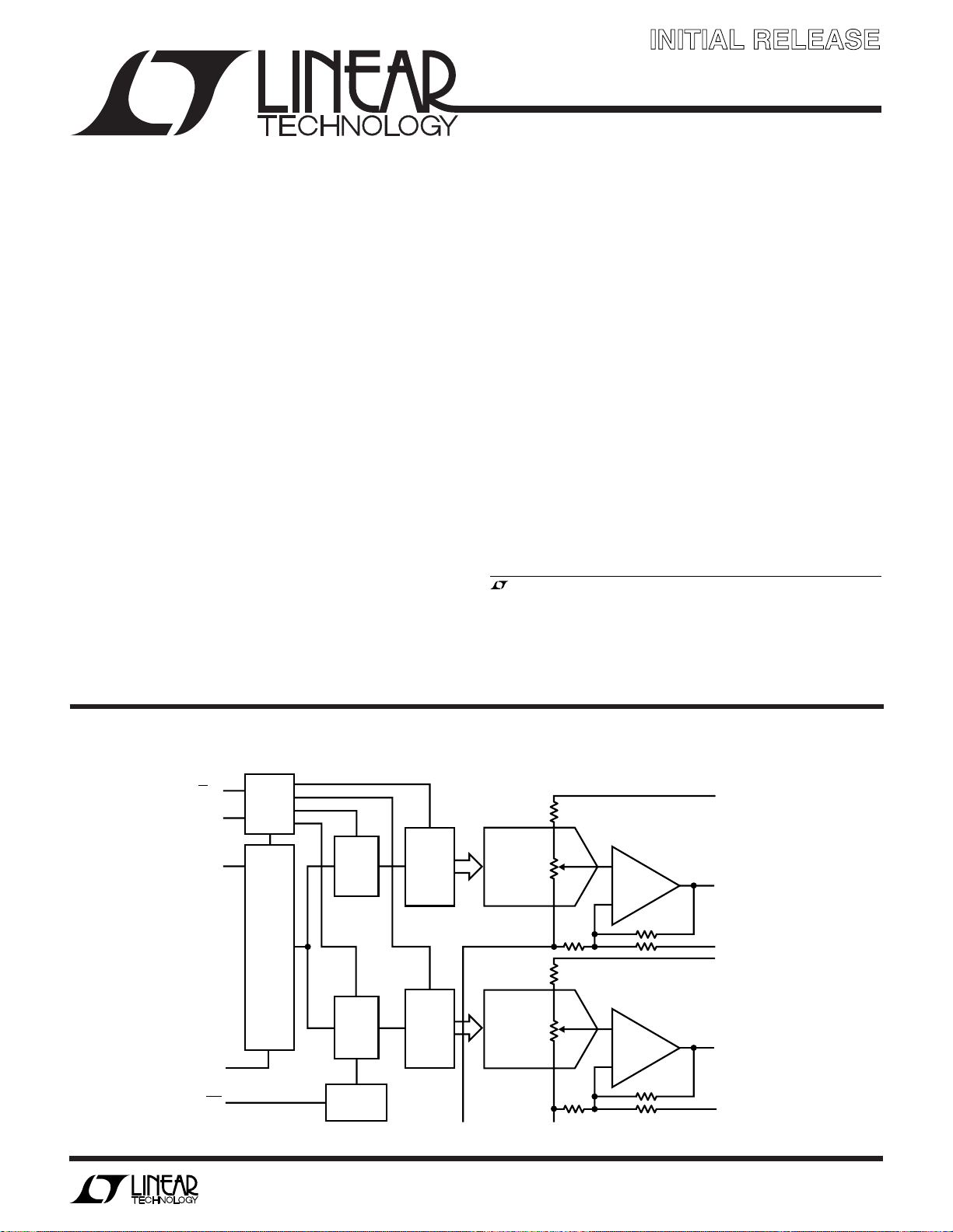
The LTC®1654 is a dual, rail-to-rail voltage output, 14-bit
digital-to-analog converter (DAC). It is available in a
16-lead narrow SSOP package, making it the smallest dual
14-bit DAC available. It includes output buffer amplifiers
and a flexible serial interface.
The LTC1654 has REFHI pins for each DAC that can be
driven up to VCC. The output will swing from 0V to VCC in
gain of 1 configuration or VCC/2 in gain of 1/2 configuration. It operates from a single 2.7V to 5.5V supply.
The LTC1654 has two programmable speeds: a FAST and
SLOW mode with ±1LSB settling times of 3.5µs or 8µs
respectively and supply currents of 750µA and 450µA in
the two modes. The LTC1654 also has shutdown capability, power-on reset and clear function to 0V.
, LTC and LT are registered trademarks of Linear Technology Corporation.
BLOCK DIAGRA
CS/LD
SCK
SDI
SDO
CLR
CONTROL
LOGIC
32-BIT
SHIFT
REGISTER
W
INPUT
LATCH
INPUT
LATCH
POWER-ON
RESET
DAC
REGISTER
DAC
REGISTER
DAC B
DAC A
REFHI B
+
V
OUT B
–
X1/X
B
1/2
REFHI A
+
V
OUT A
–
A
X
1/X1/2
REFLO AREFLO B
1654 BD
Information furnished by Linear Technology Corporation is believed to be accurate and reliable.
However, no responsibility is assumed for its use. Linear Technology Corporation makes no representation that the interconnection of its circuits as described herein will not infringe on existing patent rights.
1

LTC1654
WWWU
ABSOLUTE AXI U RATI GS
(Note 1)
VCC to GND .............................................. –0.5V to 7.5V
TTL Input Voltage, REFHI,
REFLO, X1/X
V
, SDO .................................. –0.5V to (VCC + 0.5V)
OUT
Operating Temperature Range
LTC1654C ............................................. 0°C to 70°C
LTC1654I ........................................ –40°C to 85°C
Maximum Junction Temperature ..........................125°C
Storage Temperature Range ................ –65°C to 150°C
Lead Temperature (Soldering, 10 sec)................. 300°C
ELECTRICAL CHARACTERISTICS
ture range, otherwise specifications are at TA = 25°C, VCC = 2.7V to 5.5V, V
(VCC = 5V), REFHI A, REFHI B = 2.048V (VCC = 2.7V), REFLO = 0V, X1/X
........................................ –0.5V to 7.5V
1/2
The ● denotes specifications which apply over the full operating tempera-
PACKAGE/ORDER I FOR ATIO
X
1/X1/2
X
1/X1/2
Consult factory for Military grade parts.
= 0V.
1/2
TOP VIEW
1
B
2
CLR
3
SCK
4
SDI
5
CS/LD
6
DGND
7
SDO
8
A
GN PACKAGE
16-LEAD NARROW PLASTIC SSOP
T
= 125°C, θJA = 95°C/W
JMAX
OUT A
, V
unloaded, REFHI A, REFHI B = 4.096V
OUT B
16
15
14
13
12
11
10
9
UU
W
ORDER PART
NUMBER
V
CC
V
OUT B
REFHI B
REFLO B
AGND
REFLO A
REFHI A
V
OUT A
LTC1654CGN
LTC1654IGN
GN PART MARKING
1654
1654I
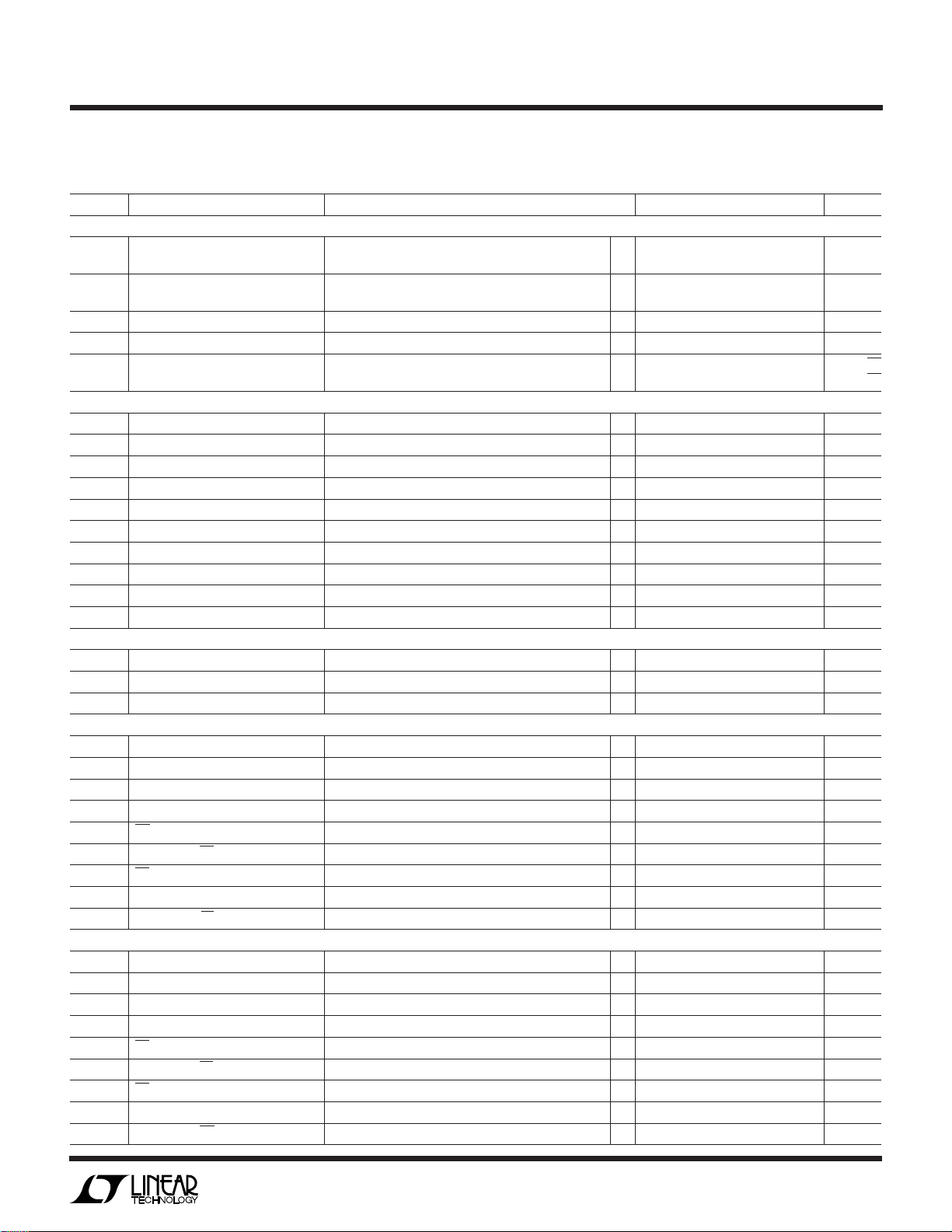
SYMBOL PARAMETER CONDITIONS MIN TYP MAX UNITS
DAC
Resolution ● 14 Bits
Monotonicity ● 14 Bits
DNL Differential Nonlinearity Guaranteed Monotonic (Note 2) ● ±1 LSB
INL Integral Nonlinearity Integral Nonlinearity (Note 2) ● ±4 LSB
ZSE Zero Scale Error C Grade ● 0 6.5 mV
V
OS
VOSTC Offset Error Tempco ±15 µV/°C
Power Supply
V
CC
I
CC
Op Amp DC Performance
Offset Error Measured at Code 50, C Grade ● ±6.5 mV
Gain Error ● ±15 LSB
Gain Error Drift 5 ppm/°C
Positive Supply Voltage For Specified Performance ● 2.7 5.5 V
Supply Current (SLOW/FAST) 2.7V ≤ VCC ≤ 5.5V (Note 5) SLOW ● 450 800 µA
Short-Circuit Current Low V
Short-Circuit Current High V
Output Impedance to GND Input Code = 0 ● 40 200 Ω
Output Line Regulation Input Code = 16383, VCC = 2.7V to 5.5V, ● 2.25 mV/V
I Grade
Measured at Code 50, I Grade ● ±9.0 mV
2.7V ≤ VCC ≤ 5.5V (Note 5) FAST ● 750 1300 µA
2.7V ≤ V
2.7V ≤ V
In Shutdown (Note 5) ● 730 µA
OUT
OUT
V
REF
≤ 3.3V (Note 5) SLOW ● 250 500 µA
CC
≤ 3.3V (Note 5) FAST ● 450 900 µA
CC
Shorted to GND ● 70 120 mA
Shorted to V
= 2.048V
CC
● 9.0 mV
● 80 120 mA
2
LTC1654
ELECTRICAL CHARACTERISTICS
ture range, otherwise specifications are at TA = 25°C, VCC = 2.7V to 5.5V, V
(VCC = 5V), REFHI A, REFHI B = 2.048V (VCC = 2.7V), REFLO = 0V, X1/X
The ● denotes specifications which apply over the full operating tempera-
1/2
OUT A
= 0V.
, V
unloaded, REFHI A, REFHI B = 4.096V
OUT B
SYMBOL PARAMETER CONDITIONS MIN TYP MAX UNITS
AC Performance
Voltage Output Slew Rate (Note 3) SLOW ● 0.20 V/µs
(Note 3) FAST
● 1.25 V/µs
Voltage Output Settling Time (Note 4) to ±1LSB, SLOW 8.0 µs
(Note 4) to ±1LSB, FAST 3.5 µs
Digital Feedthrough (Note 8) 1 nV•s
Midscale Glitch Impulse DAC Switch Between 8000 and 7FFF 20 nV•s
Output Noise Voltage Density at 1kHz, SLOW 540 nV/√Hz
at 1kHz, FAST 320 nV/√Hz
Digital I/O
V
IH
V
IL
V
OH
V
OL
V
IH
V
IL
V
OH
V
OL
I
LEAK
C
IN
Digital Input High Voltage VCC = 5V ● 2.4 V
Digital Input Low Voltage VCC = 5V ● 0.8 V
Digital Output High Voltage VCC = 5V, I
Digital Output Low Voltage VCC = 5V, I
= –1mA, D
OUT
= 1mA, D
OUT
Only ● VCC – 0.75 V
OUT
Only ● 0.4 V
OUT
Digital Input High Voltage VCC = 3V ● 2.4 V
Digital Input Low Voltage VCC = 3V ● 0.8 V
Digital Output High Voltage VCC = 3V, I
Digital Output Low Voltage VCC = 3V, I
Digital Input Leakage VIN = GND to V
= –1mA, D
OUT
= 1mA, D
OUT
CC
Only ● VCC – 0.75 V
OUT
Only ● 0.4 V
OUT
● ±10 µA
Digital Input Capacitance (Note 6) 10 pF
Reference Input
Reference Input Resistance REFHI to REFLO ● 30 60 kΩ
Reference Input Range (Notes 6, 7) ● 0VCCV
Reference Input Current In Shutdown ● 1 µA
Switching Characteristics (VCC = 4.5V to 5.5V)
t
1
t
2
t
3
t
4
t
5
t
6
t
7
t
8
t
9
SDI Valid to SCK Setup ● 30 ns
SDI Valid to SCK Hold (Note 6) ● 0ns
SCK High Time (Note 6) ● 15 ns
SCK Low Time (Note 6) ● 15 ns
CS/LD Pulse Width (Note 6) ● 15 ns
LSB SCK to CS/LD (Note 6) ● 10 ns
CS/LD Low to SCK (Note 6) ● 10 ns
SD0 Output Delay C
= 100pF ● 5 100 ns
LOAD
SCK Low to CS/LD Low (Note 6) ● 10 ns
Switching Characteristics (VCC = 2.7V to 5.5V)
t
1
t
2
t
3
t
4
t
5
t
6
t
7
t
8
t
9
SDI Valid to SCK Setup ● 45 ns
SDI Valid to SCK Hold (Note 6) ● 0ns
SCK High Time (Note 6) ● 20 ns
SCK Low Time (Note 6) ● 20 ns
CS/LD Pulse Width (Note 6) ● 20 ns
LSB SCK to CS/LD (Note 6) ● 15 ns
CS/LD Low to SCK (Note 6) ● 15 ns
SDO Output Delay C
= 100pF ● 5 150 ns
LOAD
SCK Low to CS/LD Low (Note 6) ● 15 ns
3
LTC1654
ELECTRICAL CHARACTERISTICS
Note 1: Absolute Maximum Ratings are those values beyond which the life
of a device may be impaired.
Note 2: Nonlinearity is defined from code 50 to code 16383 (full scale).
See Applications Information.
Note 3: 100pF Load Capacitor
Note 4: DAC switched between code 200 and code 16383.
U
UU
PI FU CTIO S
X1/X
1/2 Pin. When this pin is tied to V
up to REFHI/2 and when this pin is tied to REFLO, the
output will swing up to REFHI. These pins should not be
left floating.
CLR (Pin 2): The Asynchronous Clear Input.
SCK (Pin 3): The TTL Level Input for the Serial Interface
Clock.
SDI (Pin 4): The TTL Level Input for the Serial Interface
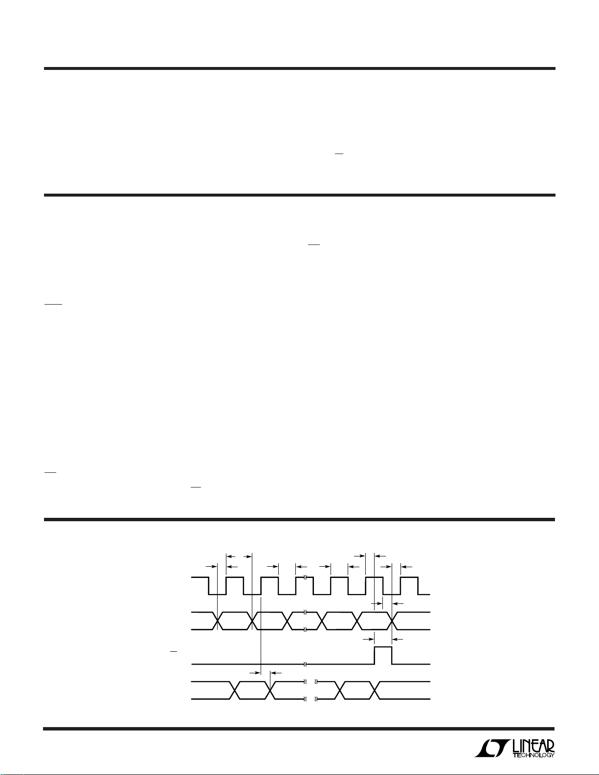
Data. Data on the SDI pin is latched into the shift register
on the rising edge of the serial clock. The LTC1654 requires a 24-bit word. The first 8 bits are control/address
followed by 16 data bits. The last two of the 16 data bits are
don’t cares. If daisy-chaining is desired, then a 32-bit data
word can be used with the first 8 being don’t cares and the
following 24 bits as above.
CS/LD (Pin 5): The TTL Level Input for the Serial Interface
Enable and Load Control. When CS/LD is low, the SCK
B, X1/X
1/2
A (Pins 1, 8): The Gain of 1 or Gain of
1/2
, the output will swing
OUT
Note 5: Digital inputs at 0V or VCC.
Note 6: Guaranteed by design.
Note 7: V
when output is unloaded. See Applications Information.
Note 8: CS/LD = 0, V
can only swing from (GND +VOS) to (VCC –VOS)
OUT
= 4.096 and data is being clocked in.
OUT
signal is enabled, so the data can be clocked in. When
CS/LD is pulled high, the control/address bits are
decoded.
DGND/AGND (Pins 6, 12): Digital and Analog Grounds.
SDO (Pin 7): The output of the shift register that becomes
valid on the rising edge of the serial clock.
V
OUT A/B
(Pins 9, 15): The Buffered DAC Outputs.
REFHI A/B (Pins 10, 14): The Reference High Inputs of the
LTC1654. There is a gain of 1 from this pin to the output
in a gain of 1 configuration. In a gain of 1/2 configuration,
there is a gain of 1/2 from this pin to V
OUT
.
REFLO A/B (Pins 11, 13): The Reference Low Inputs of the
LTC1654.
VCC (Pin 16): The Positive Supply Input. 2.7V ≤ VCC ≤ 5.5V.
Requires a 0.1µF bypass capacitor to ground.
UW
W
TI I G DIAGRA S
SCK
SDI
CS/LD
SDO
4
t
2
t
1
XX
(PREVIOUS
WORD)
t
4
XXXX
t
8
B0C3
C3 X X
t
t
3
6
t
7
t
9
t
5
CURRENT WORD
X
1654 TD01
 Loading...