

Linear Technology LTC1647-2, LTC1647-1, LTC1647-3 Datasheet
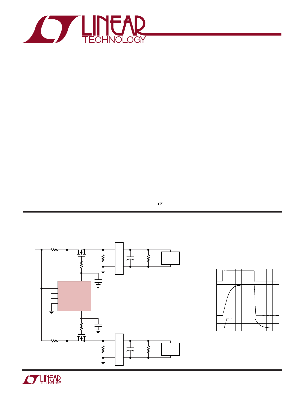
5ms/DIV
2.5V/DIV
1647-1/2/3 TA01a
V
ON
V
GATE
V
OUT
FEATURES
LTC1647-1/LTC1647-2/LTC1647-3
Dual Hot Swap Controllers
U
DESCRIPTIO
■
Allows Safe Board Insertion and Removal from a
Live Backplane
■
Programmable Electronic Circuit Breaker
■
FAULT Output Indication
■
Programmable Supply Voltage Power-Up Rate
■
High Side Drive for External MOSFET Switches
■
Controls Supply Voltages from 2.7V to 16.5V
■
Undervoltage Lockout
U
APPLICATIO S
■
Hot Board Insertion
■
Electronic Circuit Breaker
■
Portable Computer Device Bays
■
Hot Plug Disk Drive
The LTC®1647-1/LTC1647-2/LTC1647-3 are dual Hot
SwapTM controllers that permit a board to be safely inserted and removed from a live backplane.
Using external N-channel MOSFETs, the board supply
voltages can be ramped up at a programmable rate. A high
side switch driver controls the MOSFET gates for supply
voltages ranging from 2.7V to 16.5V. A programmable
electronic circuit breaker protects against overloads and
shorts. The ON pins are used to control board power or
clear a fault.
The LTC1647-1 is a dual Hot Swap controller with a
common VCC pin, separate ON pins and is available in an
SO-8 package. The LTC1647-2 is similar to the LTC1647-1
but combines a fault status flag with automatic retry at the
ON pins and is also available in the SO-8 package. The
LTC1647-3 has individual VCC pins, ON pins and FAULT
status pins for each channel and is available in a 16-lead
narrow SSOP package.
, LTC and LT are registered trademarks of Linear Technology Corporation.
Hot Swap is a trademark of Linear Technology Corporation.
TYPICAL APPLICATIO
3.3V V
SUPPLY
R1
ON1
ON2
0.1Ω
R5
0.1Ω
1
2
3
4
SENSE 1
V
CC
ON1
ON2
GND
SENSE 2
ID
Q1
1/2 MMDF3N02HD
R2
10Ω
86
GATE 1
LTC1647-1
GATE 2
75
R6
10Ω
Q2
1/2 MMDF3N02HD
U
VID Controller for Two Device Bays
DEVICE #1
R3** R4**C
C1
4.7nF
*C
** R3, R4, R7 AND R8 ARE OPTIONAL DISCHARGE
C3
4.7nF
R7** R8**C
+
CONNECTOR #1
IS USER-SELECTED BASED
LOAD
ON THE DEVICE REQUIREMENTS
RESISTORS WHEN DEVICES ARE POWERED-OFF
Q1, Q2: ON SEMICONDUCTOR
+
CONNECTOR #2
LOAD
DEVICE #2
LOAD
*
*
1394 PHY
AND/OR
USB PORT
1394 PHY
AND/OR
USB PORT
1647-1/2/3 TA01
ON/OFF Sequence
1
LTC1647-1/LTC1647-2/LTC1647-3
WW
W
U
ABSOLUTE AXI U RATI GS
(Note 1)
Supply Voltage (VCC) ............................................... 17V
Input Voltage (SENSE)................. –0.3V to (VCC + 0.3V)
Input Voltage (ON).....................................–0.3V to 17V
Output Voltage (FAULT).............................–0.3V to 17V
Output Voltage (GATE) ......... Internally Limited (Note 3)
UUW
PACKAGE/ORDER I FOR A TIO
TOP VIEW
V
1
CC
ON1
2
ON2
3
GND
4
8-LEAD PLASTIC SO
T
JMAX
8
7
6
5
S8 PACKAGE
= 150°C, θJA = 130°C/W
SENSE 1
SENSE 2
GATE 1
GATE 2
V
ON1/FAULT 1
ON2/FAULT 2
GND
T
1
CC
2
3
4
S8 PACKAGE
8-LEAD PLASTIC SO
= 150°C, θJA = 130°C/W
JMAX
Operating Temperature Range
Commercial .............................................0°C to 70°C
Industrial ............................................ –40°C to 85°C
Storage Temperature Range................. –65°C to 150°C
Lead Temperature (Soldering, 10 sec)..................300°C
1
2
3
4
5
6
7
8
TOP VIEW
16
15
14
13
12
11
10
9
V
SENSE 1
SENSE 2
GATE 1
GATE 2
NC
NC
NC
TOP VIEW
8
7
6
5
SENSE 1
SENSE 2
GATE 1
GATE 2
V
CC1
ON1
FAULT 1
ON2
FAULT 2
NC
NC
GND
CC2
GN PACKAGE
16-LEAD PLASTIC SSOP
T
= 150°C, θJA = 130°C/W
JMAX
ORDER PART NUMBER
LTC1647-1CS8
LTC1647-1IS8
S8 PART MARKING
16471
16471I
ORDER PART NUMBER
LTC1647-2CS8
LTC1647-2IS8
S8 PART MARKING
16472
16472I
ORDER PART NUMBER
LTC1647-3CGN
LTC1647-3IGN
GN PART MARKING
16473
16473I
Consult factory for Military grade parts.
ELECTRICAL CHARACTERISTICS
The ● denotes the specifications which apply over the full operating
temperature range, otherwise specifications are at TA = 25°C. VCC = 5V unless otherwise noted. (Note 2)
SYMBOL PARAMETER CONDITIONS MIN TYP MAX UNITS
V
I
I
V
V
V
I
CC
CC
CCX
LKO
LKH
CB
CP
V
Supply Range Operating Range ● 2.7 16.5 V
CCX
VCC Supply Current (Note 4) ON1, ON2 = V
V
Supply Current (Note 5, LTC1647-3) ONX = V
CCX
V
Undervoltage Lockout Coming Out of UVLO (Rising V
CCX
V
Undervoltage Lockout Hysteresis 210 mV
CCX
Circuit Breaker Trip Voltage VCB = V
V
CC1
= 5V, V
CCX
GATE X Output Current ONX High, FAULT X High, V
ONX Low, FAULT X High, V
ONX High, FAULT X Low, V
= V
, ICC = I
CC2
Individually Measured, ● 0.5 5 mA
= 12V or V
SENSEX
CCX
, I
CC2
– V
CC1
CCX
+ I
CC1
CC2
= 12V, V
CC1
CCX
= GND (Sourcing) ● 61014 µA
GATE
= VCC (Sinking) 50 µA
GATE
= 15V (Sinking) 50 mA
GATE
= 5V
CC2
) ● 2.30 2.45 2.60 V
● 1.0 6 mA
● 40 50 60 mV
2
LTC1647-1/LTC1647-2/LTC1647-3
ELECTRICAL CHARACTERISTICS
The ● denotes the specifications which apply over the full operating
temperature range, otherwise specifications are at TA = 25°C. VCC = 5V unless otherwise noted. (Note 2)
SYMBOL PARAMETER CONDITIONS MIN TYP MAX UNITS
∆V
V
ONHI
V
ONLO
V
ONHYST
I
IN
V
OL
I
LEAK
t
FAULT
t
RESET
t
ON
t
OFF
Note 1: Absolute Maximum Ratings are those values beyond which the life
of a device may be impaired.
Note 2: All currents into device pins are positive; all currents out of device
pins are negative. All voltages are referenced to ground unless otherwise
specified.
Note 3: An internal Zener on the GATE pins clamp the charge pump
voltage to a typical maximum operating voltage of 28V. External overdrive
of the GATE pin beyond the internal Zener voltage may damage the device.
External MOSFET Gate Drive (V
GATE
(V
GATE
GATE
– VCC), V
– VCC), V
CC1
CC1
= V
= 5V ● 10 13 17 V
CC2
= V
= 12V ● 10 15 19 V
CC2
ONX Threshold High ● 1.20 1.29 1.38 V
ONX Threshold Low ● 1.17 1.21 1.25 V
ONX Hysteresis 70 mV
ONX Input Current ON = GND or V
CC
● ±1 ±10 µA
FAULT X Output Low Voltage IO = 1mA, VCC = 5V ● 0.4 V
(LTC1647-2, LTC1647-3) I
= 5mA, VCC = 5V 0.8 V
O
FAULT X Output Leakage Current No Fault, FAULT X = VCC = 5V ±1 ±10 µA
(LTC1647-3)
Circuit Breaker Delay Time V
CCX
– V
= 0 to 100mV 0.3 µs
SENSEX
Circuit Breaker Reset Time ONX High to Low, to FAULT X High ● 50 100 µs
Turn-On Time ONX Low to High, to GATE X On 2 µs
Turn-Off Time ONX High to Low, to GATE X Off 1 µs
The GATE capacitance must be <0.15µF at maximum V
CC
pin clamp voltage is desired, use an external Zener diode.
Note 4: The total supply current I
is measured with V
CC
CC1
connected internally (LTC1647-1, LTC1647-2) or externally (LTC1647-3).
Note 5: The individual supply current I
The lower of the two supplies, V
CC1
is measured on the LTC1647-3.
CCX
and V
, will have its channel’s
CC2
current. The higher supply will carry the additional supply current of the
charge pump and the bias generator beside its channel’s current.
. If a lower GATE
and V
CC2
PIUTABLES
LTC1647-1 Pinout
PIN DESCRIPTION
1V
CC
2 ON1
3 ON2
4 GND
LTC1647-1 does not have the FAULT status feature.
LTC1647-2 Pinout
PIN DESCRIPTION
1V
CC
2 ON1 and FAULT 1
(Internally Tied Together)
3 ON2 and FAULT 2
(Internally Tied Together)
4 GND
The ONX/FAULT X must be connected to a driver via a resistor if the
autoretry feature is being used..
PIN DESCRIPTION
5 GATE 2
6 GATE 1
7 SENSE 2
8 SENSE 1
PIN DESCRIPTION
5 GATE 2
6 GATE 1
7 SENSE 2
8 SENSE 1
LTC1647-3 Pinout
PIN DESCRIPTION
1V
CC1
2 ON1
3 FAULT 1
4 ON2
5 FAULT 2
6NC
7NC
8 GND
PIN DESCRIPTION
9NC
10 NC
11 NC
12 GATE 2
13 GATE 1
14 SENSE 2
15 SENSE 1
16 V
CC2
3

LTC1647-1/LTC1647-2/LTC1647-3
UW
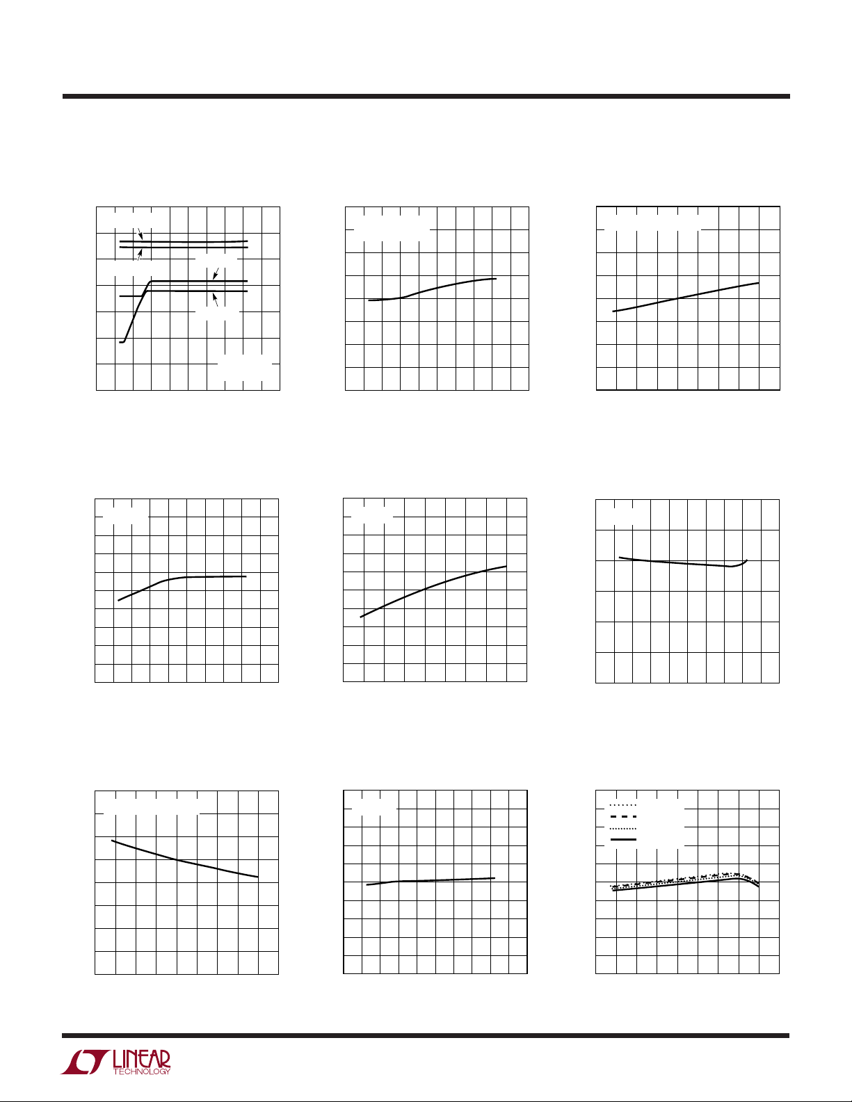
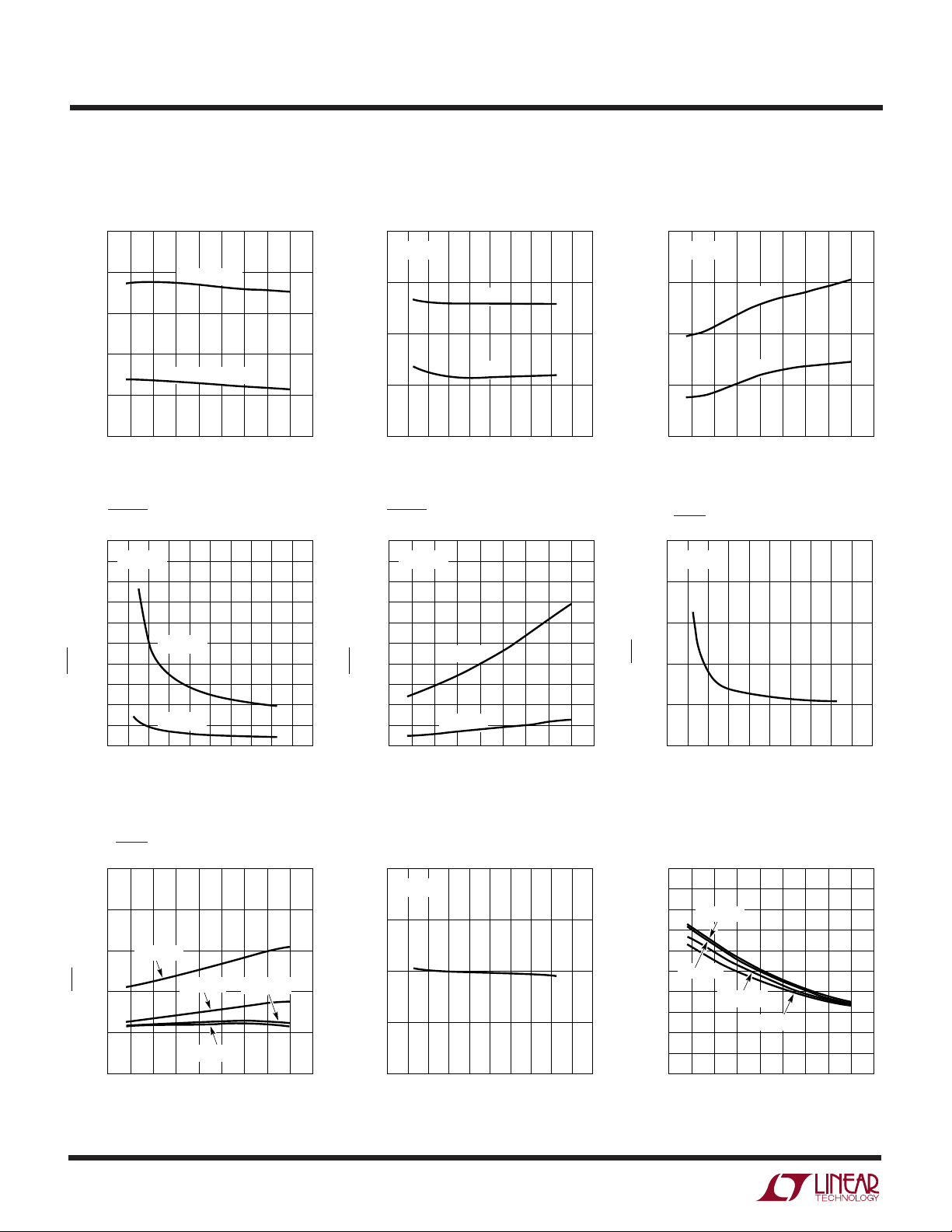
TYPICAL PERFOR A CE CHAR ACTERISTICS
ICC vs V
CC
6
TA = 25°C
= I
+ I
I
CC
CC1
5
VCC = V
4
3
(mA)
CC
I
2
1
0
2
I
vs V
CC2
5
TA = 25°C
4
3
(mA)
CC2
I
2
V
CC1
1
0
02468101214161820
CC2
= V
CC1
6 10 14 184 8 12 16
= ON1 = ON2
CC2
VCC (V)
CC2
V
= 15V
CC1
V
= 12V
CC1
= 3V
V
= 5V
CC1
V
(V)
CC2
1647-1/2/3 G01
1647-1/2/3 G04
ICC vs Temperature I
6
ICC = I
+ I
CC1
VCC = V
5
4
3
(mA)
CC
I
2
1
0
–75 –50 –25 0 25 50 75 100 125 150
(V
GATE
20
18
16
14
) (V)
12
CC
10
– V
8
GATE
(V
6
4
2
0
02468101214161820
CC2
= V
CC1
VCC = 15V VCC = 12V
VCC = 5V
– VCC) vs V
= ON1 = ON2
CC2
TEMPERATURE (°C)
CC
TA = 25°C
= V
V
CC
VCC (V)
CC1
VCC = 3V
1647-1/2/3 G02
= V
CC2
1647-1/2/3 G05
vs V
CC1
5
4
3
(mA)
CC1
I
2
1
0
02468101214161820
V
30
25
20
(V)
15
GATE
V
10
5
0
02468101214161820
TA = 25°C
V
CC1
vs V
GATE
CC2
= 15V
V
CC1
CC
V
= 5V
CC1
V
= 12V
CC1
V
VCC (V)
= 3V
CC2
(V)
TA = 25°C
V
CC
= V
CC1
1647-1/2/3 G03
= V
CC2
1647-1/2/3 G06
(V
– VCC) vs Temperature V
GATE
20
18
16
14
) (V)
12
CC
10
– V
8
GATE
(V
6
4
2
0
–75 –50 –25 0 25 50 75 100 125 150
VCC = 12V
VCC = 5V
VCC = 15V
TEMPERATURE (°C)
VCC = 3V
VCC = V
CC1
4
= V
CC2
1647-1/2/3 G07
vs Temperature (V
GATE
35
VCC = 15V
30
25
VCC = 5V
20
(V)
GATE
15
V
VCC = 3V
10
5
0
–75 –50 –25 0 25 50 75 100 125 150
TEMPERATURE (°C)
VCC = 12V
VCC = V
CC1
= V
CC2
1647-1/2/3 G08
– V
GATE1
20
V
18
CC1
16
14
) (V)
12
CC1
10
– V
8
GATE1
(V
6
V
4
2
0
02468101214161820
) vs Temperature
CC1
= 12V
V
= 5V
CC1
= 3V
CC1
V
CC2
(V)
V
CC1
= 15V
TA = 25°C
(LTC1647-3)
1647-1/2/3 G09
LTC1647-1/LTC1647-2/LTC1647-3
UW
TYPICAL PERFOR A CE CHAR ACTERISTICS
V
vs V
GATE1
35
V
30
25
V
20
(V)
GATE1
15
V
10
5
0
02468101214161820
CC1
CC1
= 15V
= 12V
CC2
V
= 5V
CC1
V
= 3V
CC1
TA = 25°C
(LTC1647-3)
V
(V)
CC2
GATE Output Sink Current vs V
100
TA = 25°C
90
80
70
60
50
40
30
20
GATE OUTPUT SINK CURRENT (µA)
10
0
02468101214161820
VCC (V)
1647-1/2/3 G10
CC
1647-1/2/3 G13
GATE Output Source Current vs
V
CC
14
TA = 25°C
13
= V
V
12
11
10
9
8
7
GATE OUTPUT SOURCE CURRENT (µA)
6
02468101214161820
=V
CC
CC1
CC2
VCC (V)
GATE Output Sink Current vs
Temperature
55
VCC = 5V
54
53
52
51
50
49
48
47
GATE OUTPUT SINK CURRENT (µA)
46
45
–75 –50 –25 0 25 50 75 100 125 150
TEMPERATURE (°C)
1647-1/2/3 G11
1647-1/2/3 G14
GATE Output Source Current vs
Temperature
14
VCC = V
13
12
11
10
9
8
7
GATE OUTPUT SOURCE CURRENT (µA)
6
–75 –50 –25 0 25 50 75 100 125 150
= V
= 5V
CC1
CC2
TEMPERATURE (°C)
GATE Fast Pull-Down Current vs
V
CC
60
TA = 25°C
55
50
45
40
35
GATE FAST PULL-DOWN CURRENT (mA)
30
02468101214161820
VCC (V)
1647-1/2/3 G12
1647-1/2/3 G15
GATE Fast Pull-Down Current vs
Temperature
80
VCC = V
70
60
50
40
30
20
10
GATE FAST PULL-DOWN CURRENT (mA)
0
–75 –50 –25 0 25 50 75 100 125 150
= V
CC1
= 5V
CC2
TEMPERATURE (°C)
1647-1/2/3 G16
Circuit Breaker Trip Voltage vs
V
CC
60
TA = 25°C
58
56
54
52
50
48
46
44
42
CIRCUIT BREAKER TRIP VOLTAGE (mV)
40
02468101214161820
VCC (V)
1647-1/2/3 G17
Circuit Breaker Trip Voltage vs
Temperature
60
58
56
54
52
50
48
46
44
42
CIRCUIT BREAKER TRIP VOLTAGE (mV)
40
–75 –50 –25 0 25 50 75 100 125 150
VCC = 15V
= 12V
V
CC
VCC = 5V
= 3V
V
CC
TEMPERATURE (°C)
1647-1/2/3 G18
5
LTC1647-1/LTC1647-2/LTC1647-3
UW
TYPICAL PERFOR A CE CHAR ACTERISTICS
Undervoltage Lockout Threshold
vs Temperature ON Threshold Voltage vs V
2.6
2.5
2.4
2.3
2.2
UNDERVOLTAGE LOCKOUT THRESHOLD (V)
2.1
–75 –50 –25 0 25 50 75 100 125 150
FAULT VOL vs V
2.0
TA = 25°C
1.8
1.6
1.4
(V)
1.2
OL
1.0
0.8
FAULT V
0.6
0.4
0.2
0
02468101214161820
RISING EDGE
FALLING EDGE
TEMPERATURE (°C)
CC
IOL = 5mA
IOL = 1mA
VCC (V)
1647-1/2/3 G19
1647-1/2/3 G22
1.35
TA = 25°C
1.30
1.25
1.20
ON THRESHOLD VOLTAGE (V)
1.15
02468101214161820
HIGH
LOW
VCC (V)
FAULT VOL vs Temperature T
2.0
VCC = 5V
1.8
1.6
1.4
(V)
1.2
OL
1.0
0.8
FAULT V
0.6
0.4
0.2
0
–75 –50 –25 0 25 50 75 100 125 150
IOL = 5mA
IOL = 1mA
TEMPERATURE (°C)
CC
1647-1/2/3 G20
1647-1/2/3 G23
ON Threshold Voltage vs
Temperature
1.35
VCC = 5V
1.30
1.25
1.20
ON THRESHOLD VOLTAGE (V)
1.15
–75 –50 –25 0 25 50 75 100 125 150
FAULT
1.0
TA = 25°C
0.8
0.6
(µs)
FAULT
T
0.4
0.2
0
02468101214161820
HIGH
LOW
TEMPERATURE (°C)
vs V
CC
VCC (V)
1647-1/2/3 G21
1647-1/2/3 G24
T
vs Temperature Circuit Breaker Reset Time vs V
FAULT
1.0
0.8
0.6
(µs)
FAULT
T
0.4
0.2
VCC = 3V
VCC = 5V
0
–75 –50 –25 0 25 50 75 100 125 150
TEMPERATURE (°C)
VCC = 12V
VCC = 15V
6
1647-1/2/3 G25
70
TA = 25°C
60
50
40
CIRCUIT BREAKER RESET TIME (µs)
30
02468101214161820
VCC (V)
CC
1647-1/2/3 G26
Circuit Breaker Reset Time vs
Temperature
60
58
56
54
52
50
48
46
44
CIRCUIT BREAKER RESET TIME (µs)
42
40
VCC = 3V
VCC = 5V
VCC = 12V
VCC = 15V
–75 –50 –25 0 25 50 75 100 125 150
TEMPERATURE (°C)
1647-1/2/3 G27
 Loading...