

Linear Technology LTC1645 Datasheet
FEATURES
LTC1645
Dual-Channel Hot Swap
Controller/Power Sequencer
U
DESCRIPTIO
■
Allows Safe Board Insertion and Removal from a
Live Backplane
■
Programmable Power Supply Sequencing
■
Programmable Electronic Circuit Breaker
■
User-Programmable Supply Voltage Power-Up and
Power-Down Rate
■
High Side Drivers for External N-Channel FETs
■
Controls Supply Voltages from 1.2V to 12V
■
Ensures Proper Power-Up Behavior
■
Undervoltage Lockout
■
Glitch Filter Protects Against Spurious RESET Signals
U
APPLICATIO S
■
Hot Board Insertion
■
Power Supply Sequencing
■
Electronic Circuit Breaker
U
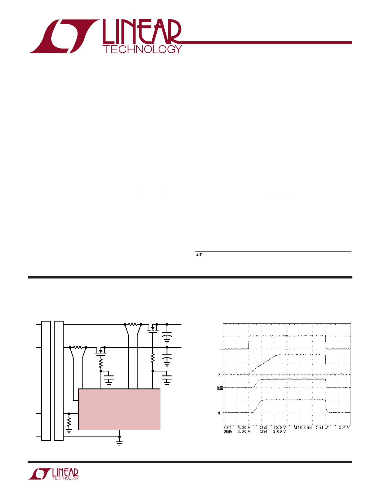
TYPICAL APPLICATIO
The LTC®1645 is a 2-channel Hot SwapTM controller that
allows a board to be safely inserted and removed from a
live backplane. Using external N-channel pass transistors,
the supply voltages can be ramped at a programmable
rate. Two high side switch drivers control the N-channel
gates for supply voltages ranging from 1.2V to 12V. The
two channels can be set to ramp up and down separately,
or they can be programmed to rise and fall simultaneously,
ensuring power supply tracking at the two outputs.
Programmable electronic circuit breakers protect against
shorts at either output. The RESET output can be used to
generate a system reset when a supply voltage falls below
a user-programmed voltage. An additional spare comparator is available for monitoring a second supply
voltage.
The LTC1645 is available in the 8- and 14-pin SO packages.
, LTC and LT are registered trademarks of Linear Technology Corporation.
Hot Swap is a trademark of Linear Technology Corporation.
V
IN2
V
IN1
ON
GND
CONNECTOR 1
CONNECTOR 2
PLUG-IN CARDBACKPLANE
5V and 3.3V Hot Swap
0.005Ω*
10k
IRF7413
10Ω
6
7
GATE1 SENSE2
SENSE1 V
8
V
CC1
5
ON
0.01µF
25V
LTC1645
(8-LEAD)
GND
4
0.005Ω*
CC2
IRF7413
10Ω
3
2
1
GATE2
*LRF1206-01-R005-J (IRC)
+
+
1645 TA01
C
LOAD2
C
LOAD1
0.01µF
25V
V
OUT2
3.3V
5A
V
OUT1
5V
5A
ON
5V/DIV
GATE
10V/DIV
V
OUT2
5V/DIV
V
OUT1
5V/DIV
5V and 3.3V Hot Swap Waveforms
n
1
LTC1645
WWWU
ABSOLUTE AXI U RATI GS
(Note 1)
Supply Voltage (V
CC1
, V
) ................................. 13.2V
CC2
Input Voltage
FB, ON, COMP+..................... –0.3V to (V
+ 0.3V)
CC1
TIMER ................................................. – 0.3V to 2.5V
SENSE1 ..................... (V
SENSE2 ...................... (V
– 0.7V) to (V
CC1
– 0.7V) to (V
CC1
+ 0.3V)
CC1
+ 0.3V)
CC2
Output Voltage
RESET, COMPOUT, FAULT .....................–0.3V to 16V
GATE1, GATE2................. Internally Limited (Note 3)
UU
W
PACKAGE/ORDER I FOR ATIO
ORDER PART
NUMBER
LTC1645CS8
LTC1645IS8
S8 PART MARKING
1645
1645I
V
CC2
SENSE2
GATE2
GND
TOP VIEW
1
2
3
4
S8 PACKAGE
8-LEAD PLASTIC SO
T
= 125°C, θJA = 150°C/W
JMAX
8
7
6
5
V
CC1
SENSE1
GATE1
ON
Output Current
GATE1, GATE2............................................... ±20mA
Operating Temperature Range
LTC1645C ............................................... 0°C to 70°C
LTC1645I............................................ –40°C to 85°C
Storage Temperature Range ................. –65°C to 150°C
Lead Temperature (Soldering, 10 sec).................. 300°C
ORDER PART
NUMBER
LTC1645CS
LTC1645IS
V
CC2
SENSE2
GATE2
FAULT
RESET
GND
TOP VIEW
1
2
3
4
5
6
FB
7
S PACKAGE
14-LEAD PLASTIC SO
T
= 125°C, θJA = 110°C/W
JMAX
14
13
12
11
10
9
8
V
CC1
SENSE1
GATE1
TIMER
ON
COMPOUT
+
COMP
Consult factory for Military grade parts.
ELECTRICAL CHARACTERISTICS
The ● denotes the specifications which apply over the full operating temperature range, otherwise specifications are at TA = 25°C.
2.375V ≤ V
SYMBOL PARAMETER CONDITIONS MIN TYP MAX UNITS
DC Characteristics
I
CC1
I
CC2
V
LKO1
V
LKO2
V
LKH
n
V
FB
∆V
FB
V
FBHST
V
COMP
∆V
COMP
V
COMPHST
≤ 12V, 1.2V ≤ V
CC1
V
Supply Current ON = V
CC1
V
Supply Current ON = V
CC2
V
Undervoltage Lockout High to Low ● 2.16 2.23 2.3 V
CC1
V
Undervoltage Lockout High to Low ● 1.06 1.12 1.18 V
CC2
V
Undervoltage Lockout Hysteresis 25 mV
CCn
FB Pin Voltage Threshold High to Low ● 1.226 1.238 1.250 V
FB Pin Threshold Line Regulation High to Low, V
FB Pin Voltage Threshold Hysteresis 5 mV
COMP+ Pin Voltage Threshold High to Low ● 1.226 1.238 1.250 V
COMP+ Pin Threshold Line Regulation High to Low, V
COMP+ Pin Voltage Threshold Hysteresis 5 mV
≤ 12V unless otherwise noted (Note 2).
CC2
= 5V, V
CC1
= 5V, V
CC1
= 3.3V ● 1.1 2.0 mA
CC2
= 3.3V ● 0.28 0.4 mA
CC2
= 2.375V to 12V ● 14 mV
CC1
= 2.375V to 12V ● 14 mV
CC1
2
LTC1645
TEMPERATURE (°C)
–40
0.8
1.0
1.4
20 60
1645 G03
0.6
0.4
–20 0
40 80 100
0.2
0
1.2
I
CC
n
(mA)
V
CC1
= 5V
V
CC2
= 3.3V
I
CC1
I
CC2
ELECTRICAL CHARACTERISTICS
The ● denotes the specifications which apply over the full operating temperature range, otherwise specifications are at TA = 25°C.
2.375V ≤ V
SYMBOL PARAMETER CONDITIONS MIN TYP MAX UNITS
V
TM
∆V
TM
I
TM
V
CB1
V
CB2
t
CBD
n
I
CP
∆V
GATE
n
V
ONFPD
V
ON1
V
ON2
V
ONHYST
I
ON
V
OL
≤ 12V, 1.2V ≤ V
CC1
≤ 12V unless otherwise noted (Note 2).
CC2
TIMER Pin Voltage Threshold ● 1.212 1.230 1.248 V
TIMER Pin Threshold Line Regulation V
TIMER Pin Current Timer On, V
Circuit Breaker Trip Voltage 1 V
Circuit Breaker Trip Voltage 2 V
Circuit Breaker Trip Delay V
GATEn Pin Output Current ON = 2.2V, V
External N-Channel Gate Drive ∆V
= 2.375V to 12V ● 19 mV
CC1
Timer Off, V
= (V
CB1
CC1
= (V
CB2
CC2
= (V
CB
n
CC
ON = 0.7V, V
ON = 0.3V, V
= (V
GATE
n
= 0.6V, V
TIMER
= 1.5V 12 mA
TIMER
– V
SENSE1
– V
SENSE2
– V
n
SENSE
= V
GATE
n
= V
GATE
n
= V
GATE
n
– V
GATE
n
= 5V ● –2.3 –2 –1.7 µA
CC1
) ● 46 50 56 mV
) ● 46 50 56 mV
) > 60mV 1.5 µs
n
, V
CC
CC
CC
= 5V, V
n
CC1
, V
= 5V, V
n
CC1
, V
= 5V, V
n
CC1
) ● 4.5 16 V
CC
n
= 3.3V ● –12.5 –10 –7.5 µA
CC2
= 3.3V ● 30 40 50 µA
CC2
= 3.3V 12 mA
CC2
ON Pin Fast Pull-Down Threshold Low to High ● 0.375 0.4 0.425 V
High to Low, Fast Pull-Down Engaged
● 0.35 0.375 0.4 V
ON Pin Threshold #1 Low to High, GATE1 Turns On ● 0.8 0.825 0.85 V
High to Low, GATE1 Turns Off
● 0.775 0.8 0.825 V
ON Pin Threshold #2 Low to High, GATE2 Turns On ● 2 2.025 2.050 V
High to Low, GATE2 Turns Off
● 1.975 2 2.025 V
ON Pin Hysteresis 25 mV
ON Pin Input Current V
Output Low Voltage RESET, FAULT, COMPOUT, I
CC1
= 5V, V
= 3.3V ● ±0.01 ±2 µA
CC2
= 1.6mA, V
OUT
= 5V ● 0.16 0.4 V
CC1
Note 1: Absolute Maximum Ratings are those values beyond which the life
of a device may be impaired.
Note 2: All currents into device pins are positive; all currents out of device
pins are negative. All voltages are referenced to ground unless otherwise
specified.
Note 3: An internal zener on the GATEn pins clamps the charge pump
voltage to a typical maximum operating voltage of 22V. External overdrive
of a GATE pin (for example, from capacitive coupling of V
beyond the internal zener voltage may damage the device. If a lower
GATEn pin clamp voltage is desired, use an external zener diode.
UW
TYPICAL PERFOR A CE CHARACTERISTICS
V
Supply Current vs Voltage V
CC1
3.0
TA = 25°C
2.5
2.0
(mA)
1.5
CC1
I
1.0
0.5
0
= 1.5V
V
CC2
V
= 12V
CC2
46810
V
(V)
CC1
123257911
1645 G01
3.5
3.0
2.5
2.0
(mA)
CC2
1.5
I
1.0
0.5
Supply Current vs Voltage
CC2
TA = 25°C
V
= 2.375V
CC1
0
3
5
68
4
2
1
V
CC2
(V)
V
CC1
7
= 12V
9
10 11 12
1645 G02
glitches)
CC
n
Supply Current vs Temperature
3
LTC1645
FEEDBACK TRANSIENT (mV)
0
0
GLITCH FILTER TIME (µs)
10
30
40
50
100
70
80
160
200
1645 G06
20
80
90
60
40
120
240
280
TA = 25°C
UW
TYPICAL PERFOR A CE CHARACTERISTICS
GATE Voltage vs Supply Voltage
25
TA = 25°C
20
15
(V)
n
GATE
10
5
0
4
5
311
2
HIGHEST VCC (V)
8
6
7
9
10
12
1645 G04
GATE Voltage vs Temperature
16.0
V
= 5V
CC1
15.8
15.6
15.4
15.2
(V)
n
15.0
GATE
14.8
14.6
14.4
14.2
14.0
–40
= 3.3V
V
CC2
40
20
0
–20
TEMPERATURE (°C)
60
80
Glitch Filter Time
vs Feedback Transient
100
1645 G05
RESET, FAULT, COMPOUT Output
Voltage vs Temperature
450
V
= 5V
CC1
400
350
300
250
200
150
OUTPUT VOLTAGE (mV)
100
50
0
SINK CURRENT = 3mA
SINK CURRENT = 1.6mA
–20 0 20 100
–40
TEMPERATURE (°C)
40 60 80
1645 G07
RESET, FAULT, COMPOUT Output
Voltage vs V
800
700
600
500
400
300
OUTPUT VOLTAGE (mV)
200
100
SINK CURRENT = 1.6mA
0
2
CC1
SINK CURRENT = 3mA
468 129357 11
V
(V)
CC1
TA = 25°C
10
1645 G08
Fast Pull-Down Current vs V
18
TA = 25°C
17
= 1.5V
V
CC2
16
15
14
13
12
11
10
FAST PULL-DOWN CURRENT (mA)
9
8
4
23 5 9 11
687
V
CC1
(V)
CC1
10
12
1645 G09
4

LTC1645
U
PI FU CTIO S
V
(Pin 1/Pin 1): Positive Supply Input. V
CC2
from 1.2V to 12V for normal operation. I
0.2mA. An undervoltage lockout circuit disables the
LTC1645 whenever the voltage at V
SENSE2 (Pin 2/Pin 2): V
a sense resistor placed in the supply path between V
and SENSE2, the circuit breaker trips when the voltage
across the resistor exceeds 50mV for more than 1.5µs. If
the circuit breaker trip current is set to twice the normal
operating current, only 25mV is dropped across the sense
resistor during normal operation. To disable the circuit
breaker, short V
GATE2 (Pin 3/Pin 3): Channel 2 High Side Gate Drive.
Connect to the gate of an external N-channel MOSFET. An
internal charge pump guarantees at least 4.5V of gate
drive. The charge pump is powered by the higher of V
and V
on by connecting a 10µA current source from the charge
pump output to the GATE2 pin and the voltage starts to
ramp up with a slope dv/dt = 10µA/C
pin is below 2V but above 0.4V, a 40µA current source
pulls GATE2 toward ground. If the ON pin is below 0.4V,
the circuit breaker trips or the undervoltage lockout circuit
trips, the GATE2 pin is immediately pulled to ground with
a 12mA (typ) current source.
FAULT (Pin 4/NA): Circuit Breaker Fault. FAULT is an
open-drain output that pulls low when the circuit breaker
function trips. The circuit breaker is reset by pulling the ON
pin below 0.4V. An external pull-up is required to generate
a logic high at the FAULT pin. When the ON pin is low,
FAULT will release.
The circuit breaker can be programmed to automatically
reset by connecting the FAULT pin to the ON pin. In this
circuit configuration, if a logic device is driving the ON pin,
use a series resistor between the logic output and the ON
pin to prevent large currents from flowing.
RESET (Pin 5/NA): Open-Drain RESET Output. The RESET
pin is pulled low when the voltage at the FB pin goes below
1.238V or V
old. The RESET pin goes high one timing cycle after the
voltage at the FB pin goes above the FB pin threshold. The
ON pin must remain above 0.8V during this timing cycle.
. When the ON pin exceeds 2V, GATE2 is turned
CC2
is below the undervoltage lockout thresh-
CC1
UU
(14-Lead Package/8-Lead Package)
CC2
Circuit Breaker Set Pin. With
CC2
and SENSE2 together.
CC2
can range
CC2
is typically
CC2
is less than 1.12V.
. While the ON
GATE2
CC2
CC1
An external pull-up is required to generate a logic high at
the RESET pin.
FB (Pin 6/NA): RESET Comparator Input. The FB pin is
used to monitor the output supply voltage with an external
resistive divider. When the voltage on the FB pin is lower
than 1.238V, the RESET pin is pulled low. A glitch filter on
the FB pin prevents fast transients from forcing RESET
low. When the voltage on the FB pin rises above the trip
point, the RESET pin goes high after one timing cycle.
GND (Pin 7/Pin 4): Ground. Connect to a ground plane for
optimum performance.
COMP+ (Pin 8/NA): Spare Comparator Noninverting Input. When the voltage on COMP+ is lower than 1.238V,
COMPOUT pulls low.
COMPOUT (Pin 9/NA): Open-Drain Spare Comparator
Output. COMPOUT pulls low when the voltage on COMP
is below 1.238V or V
threshold. An external pull-up is required to generate a
logic high at the COMPOUT pin.
ON (Pin 10/Pin 5): Analog Control Input. If the ON pin
voltage is below 0.4V, both GATE1 and GATE2 are immediately pulled to ground. While the voltage is between 0.4V
and 0.8V, both GATE1 and GATE2 are each pulled to
ground with a 40µA current source. While the voltage is
between 0.8V and 2V, the GATE1 pull-up is turned on after
one timing cycle, but GATE2 continues to be pulled to
ground with a 40µA current source. When the voltage
exceeds 2V, both the GATE1 and GATE2 pull-ups are
turned on one timing cycle after the voltage exceeds 0.8V.
The ON pin is also used to reset the electronic circuit
breaker. If the ON pin is brought below and then above
0.4V following the trip of the circuit breaker, the circuit
breaker resets, and a normal power-up sequence occurs.
TIMER: (Pin 11/NA): System Timing Pin. The TIMER pin
requires an external capacitor to ground to generate a
timing delay. The pin is used to set the delay before the
RESET pin goes high after the output supply voltage is
good as sensed by the FB pin. It is also used to set the delay
between the ON pin exceeding 0.8V and the GATE1 and
GATE2 pins turning on (GATE2 turns on only if the ON pin
exceeds 2V).
is below the undervoltage lockout
CC1
+
5
LTC1645
U
PI FU CTIO S
UU
(14-Lead Package/8-Lead Package)
Whenever the timer is inactive, an internal N-channel FET
shorts the TIMER pin to ground. Activating the timer
connects a 2µA current source from V
to the TIMER pin
CC1
and the voltage starts to ramp up with a slope dv/dt = 2µA/
C
. When the voltage reaches the trip point (1.23V),
TIMER
the timer is reset by pulling the TIMER pin back to ground.
The timer period is (1.23V • C
TIMER
)/2µA.
GATE1 (Pin 12/Pin 6): Channel 1 High Side Gate Drive.
Connect to the gate of an external N-channel MOSFET. An
internal charge pump guarantees at least 4.5V of gate
drive. The charge pump is powered by the higher of V
and V
. When the ON pin exceeds 0.8V, GATE1 is turned
CC2
CC1
on by connecting a 10µA current source from the charge
pump output to the GATE1 pin and the voltage starts to
ramp up with a slope dv/dt = 10µA/C
. While the ON
GATE1
pin is below 0.8V but above 0.4V, a 40µA current source
pulls GATE1 toward ground. If the ON pin is below 0.4V,
the circuit breaker trips or the undervoltage lockout circuit
trips, the GATE1 pin is immediately pulled to ground with
a 12mA (typ) current source.
SENSE1 (Pin 13/Pin 7): V
a sense resistor placed in the supply path between V
Circuit Breaker Set Pin. With
CC1
CC1
and SENSE1, the circuit breaker trips when the voltage
across the resistor exceeds 50mV for more than 1.5µs. If
the circuit breaker trip current is set to twice the normal
operating current, only 25mV is dropped across the sense
resistor during normal operation. To disable the circuit
breaker, short V
V
(Pin 14/Pin 8): Positive Supply Input. V
CC1
from 2.375V to 12V for normal operation. I
and SENSE1 together.
CC1
can range
CC1
is typically
CC1
1mA. An undervoltage lockout circuit disables the chip
whenever the voltage at V
logic is powered by V
is less than 2.23V. All internal
CC1
.
CC1
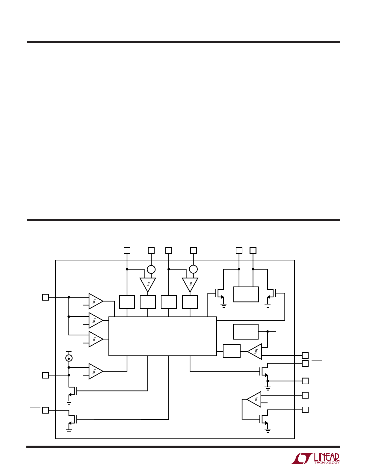
BLOCK DIAGRA
0.8V
0.4V
2µA
REF
+
–
2V
+
–
+
–
+
–
ON
TIMER
FAULT
10
11
4
W
V
CC1
14
2.23V
UVL
SENSE113V
+
1.5µs
FILTER
CC2
1
–
50mV 50mV
+
–
1.12V
UVL
LOGIC
SENSE2
+
1.5µs
FILTER
GATE112GATE2
2
–
+
–
GLITCH
FILTER
4× CHARGE
PUMP
1.238V
REFERENCE
3
REF
–
+
–
REF
+
6
5
7
8
9
FB
RESET
GND
+
COMP
COMPOUT
6
1645 BD
WUUU
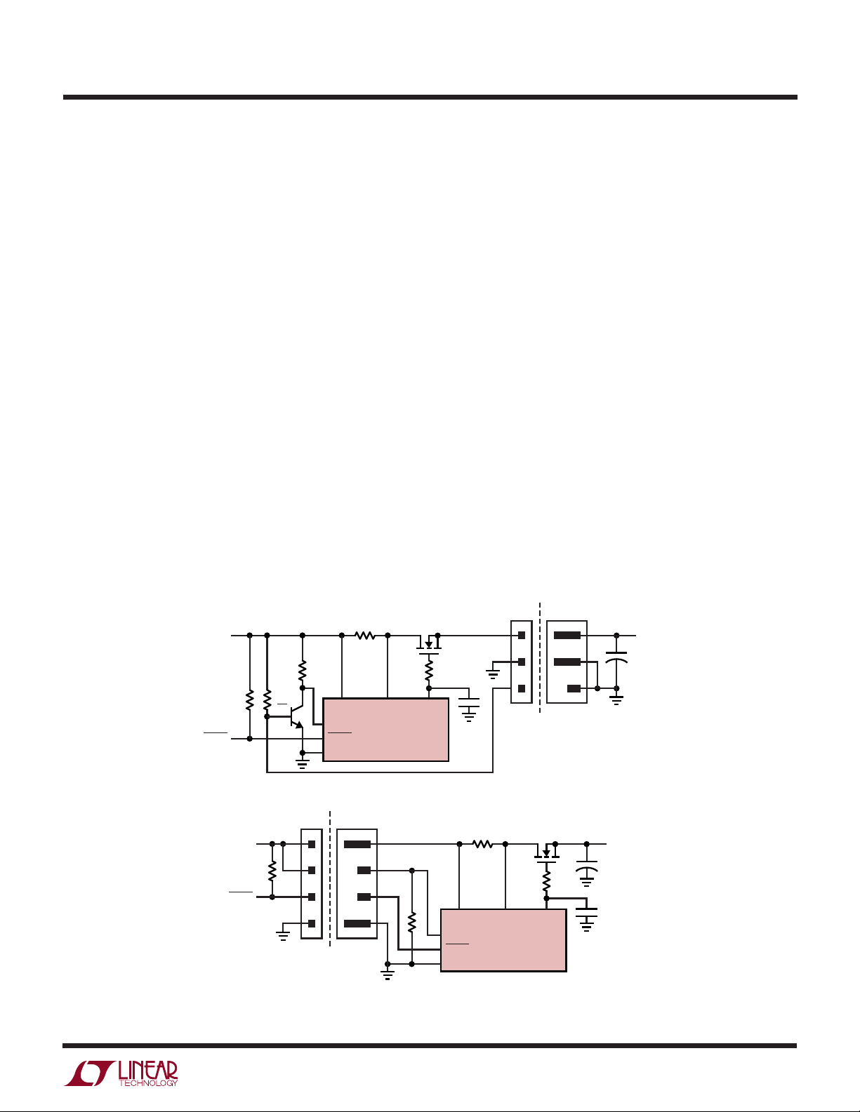
APPLICATIO S I FOR ATIO
LTC1645
Hot Circuit Insertion
When a circuit board is inserted into a live backplane, the
supply bypass capacitors on the board can draw huge
transient currents from the backplane power bus as they
charge. These transient currents can cause permanent
damage to the connector pins and produce glitches on the
system supply, resetting other boards in the system.
The LTC1645 is designed to turn a board’s supply voltages
on and off in a controlled manner, allowing the board to be
safely inserted or removed from a live backplane. The chip
provides a system reset signal and a spare comparator to
indicate when board supply voltages drop below userprogrammable voltages, and a fault signal to indicate if an
overcurrent condition has occurred.
The LTC1645 can be located before or after the connector
as shown in Figure 1. A staggered PCB connector can
sequence pin connections when plugging and unplugging
circuit boards. Alternatively, the control signal can be
generated by processor control.
Power Supply Tracking and Sequencing
Some applications require that the potential difference
between two power supplies not exceed a certain voltage.
This requirement applies during power-up and powerdown as well as during steady state operation, often to
prevent latch-up in a dual supply ASIC. Other systems
require one supply to come up after another, for example,
if a system clock needs to start before a block of logic.
Typical dual supplies or backplane connections may come
up at arbitrary rates depending on load current, capacitor
size, soft-start rates, etc. Traditional solutions are cumbersome and require complex circuitry to meet the power
supply requirements.
The LTC1645 provides a simple solution to power supply
tracking and sequencing needs. The LTC1645 guarantees
supply tracking by ramping the supplies up and down
together (see Figure 15). The sequencing capabilities of
the LTC1645 allow nearly any combination of supply
ramping (e.g., see Figure 17) to satisfy various sequencing specifications. See the Power Supply Tracking and
Sequencing Applications section for more information.
V
FAULT
CC
V
FAULT
CC
SENSE
V
ON
BACKPLANE
CONNECTOR
CC
ON
LTC1645
FAULT
GND
(a) Hot Swap Controller on Motherboard
STAGGERED PCB
EDGE CONNECTOR
(b) Hot Swap Controller on Daughterboard
GATE
V
ON
FAULT
GND
CC
BACKPLANE
CONNECTOR
SENSE
LTC1645
STAGGERED PCB
EDGE CONNECTOR
+
GATE
1645 F01
C
+
V
OUT
LOAD
C
V
LOAD
OUT
Figure 1. Staggered Pins Connection
7
LTC1645
WUUU
APPLICATIO S I FOR ATIO
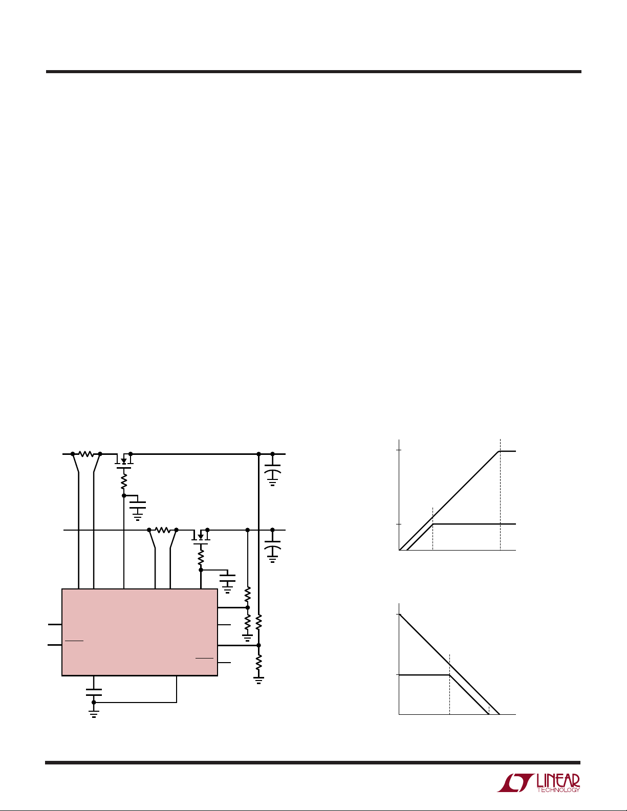
Power Supply Ramping
The power supplies on a board are controlled by placing
external N-channel pass transistors in the power paths as
shown in Figure 2. Consult Table 1 for a selection of
N-channel FETs suitable for use with the LTC1645. R
and R
SENSE2
provide current fault detection and R1 and R2
SENSE1
prevent high frequency oscillation. By ramping the gates
of the pass transistors up and down at a controlled rate,
the transient surge current (I = C • dv/dt) drawn from the
main backplane supply is limited to a safe value when the
board makes connection.
When power is first applied to the chip, the gates of the
N-channels (GATE1 and GATE2 pins) are pulled low. After
the ON pin is held above 0.8V for at least one timing cycle,
the voltage at GATE1 begins to rise with a slope equal to
dv/dt = 10µA/C1 (Figure 3), where C1 is the external
capacitor connected between the GATE1 pin and GND. If
the ON pin is brought above 2V (and the ON pin has been
held above 0.8V for at least one timing cycle), the voltage
at GATE2 begins to rise with a slope equal to dv/dt =
10µA/C2.
The ramp time for each supply is t = (V
• Cn)/10µA. If
CC
n
the ON pin is pulled below 2V for GATE2 or 0.8V for GATE1
(but above 0.4V), a 40µA current source is connected from
GATEn to GND, and the voltage at the GATEn pin will ramp
down, as shown in Figure 4.
Ringing
Good engineering practice calls for bypassing the supply
rail of any circuit. Bypass capacitors are often placed at the
supply connection of every active device, in addition to one
or more large value bulk bypass capacitors per supply rail.
If power is connected abruptly, the bypass capacitors slow
the rate of rise of voltage and heavily damp any parasitic
resonance of lead or trace inductance working against the
supply bypass capacitors.
The opposite is true for LTC1645 Hot Swap circuits on a
daughterboard. In most cases, on the powered side of the
N-channel FET switches (V
) there is no supply bypass
CC
n
capacitor present. An abrupt connection, produced by
plugging a board into a backplane connector, results in a
fast rising edge applied to the V
line of the LTC1645.
CC
n
R
CC1
CC2
10
4
SENSE1
SENSE1 GATE2
V
CC1
ON
FAULT
TIMER GND
V
V
Q1
R1
10Ω
C1
R
SENSE2
1314
(14-LEAD)
11 7
C
TIMER
12
LTC1645
1
V
SENSE2GATE1
CC2
2
COMPOUT
Q2
COMP
RESET
3
R2
10Ω
+
FB
V
+ ∆V
CCn
V
CCn
GATE
SLOPE = 10µA/C
V
CC
n
t
1
Figure 3. Supply Turning On
+ ∆V
GATE
GATE
n
V
OUT
V
CC
n
n
t
n
SLOPE = 40µA/C
3
t
V
OUT1
+
C
LOAD1
V
OUT2
+
C
LOAD2
C2
8
9
6
5
1645 F02
GATE
n
V
OUT
n
t
2
1645 F03
n
1645 F04
4
8
Figure 2. Typical Hot Swap Connection
Figure 4. Supply Turning Off
 Loading...