

Linear Technology LTC1642 Datasheet
Final Electrical Specifications
FEATURES
■
Single Channel Positive NFET Driver
■
Programmable Undervoltage and Overvoltage
Protection
■
Foldback Current Limit
■
Adjustable Current Limit Time-Out
■
Latch Off or Automatic Retry on Current Fault
■
Driver for SCR Crowbar on Overvoltage
■
Programmable Reset Timer
■
Reference Output with Uncommitted Comparator
■
VCC: 2.97V to 16.5V Normal Operation, Protected
Against Surges to 33V.
■
16-Pin SSOP Package
U
APPLICATIO S
■
Hot Board Insertion
■
Electronic Circuit Breaker
LTC1642
Hot Swap Controller
May 1999
U
DESCRIPTIO
TM
The LTC®1642 is a 16-pin Hot Swap
allows a board to be safely inserted and removed from a
live backplane. Using an external N-channel pass transistor, the board supply voltage can be ramped up at a
programmable rate. A high side switch driver controls the
N-channel gate for supply voltages ranging from 2.97V to
16.5V.
The SENSE pin allows foldback limiting of the load current,
with circuit breaker action after a programmable delay
time. The delay allows the part to power-up in current
limit. The CRWBR output can be used to trigger an SCR
for crowbar load protection after a programmable delay if
the input supply exceeds a programmable voltage. The
RESET output can be used to generate a system reset with
programmable delay when the supply voltage falls below
a programmable voltage. The ON pin can be used to cycle
the board power. The LTC1642 is available in the 16-pin
SSOP package.
, LTC and LT are registered trademarks of Linear Technology Corporation.
Hot Swap is a trademark of Linear Technology Corporation.
controller that
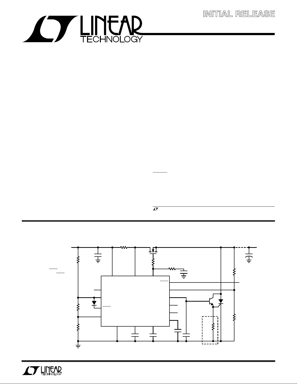
TYPICAL APPLICATIO
12V
R5
110k
1%
LATCH OFF: FLOAT FAULT
AUTOMATIC RETRY: TIE FAULT TO ON
UNDERVOLTAGE = 10.8V
R6
2.87k
1%
OVERVOLTAGE = 13.2V
R7
11.3k
RESET TIME = 200ms
CURRENT LIMIT TIME = 20ms
CROWBAR TIME = 90µs
1%
U
R1
0.010Ω
5%
C7
0.1µF
16 15 14
V
CC
10
COMPOUT
4
6
9
ON
FAULT
OV
GND BRK TMR
D1
1N4148
Information furnished by Linear Technology Corporation is believed to be accurate and reliable.
However, no responsibility is assumed for its use. Linear Technology Corporation makes no representation that the interconnection of its circuits as described herein will not infringe on existing patent rights.
SENSE GATE
LTC1642
823
C3
0.33µF
Q1
FDR9410A
R2
100Ω
5%
RST TMR
RESET
CRWBR
COMP
COMP
REF
C2
0.33µF
FB
–
+
0.1µF
R8
330Ω
5%
5
7
1
12
11
13
C5
C1
0.047µF
Q2
2N2222
220Ω
C6
0.01µF
R9 REQUIRED ONLY WITH SENSITIVE GATE SCRs,
NOT NEEDED WITH MCR12
5%
12V
AT 2.5A
+
C
LOAD
R3
107k
1%
POWER-GOOD = 11.4V
Q3
MCR
12DC
R4
13k
R9
1%
1642 TA01
1

LTC1642
WW
W
ABSOLUTE AXI U RATI GS
U
UUW
PACKAGE/ORDER I FOR A TIO
(Note 1)
Supply Voltage (VCC) .................................–0.3V to 33V
SENSE Pin ................................... –0.3V to (VCC + 0.3V)
GATE Pin ...................................................–0.3V to 27V
All Other Pins..........................................–0.3V to 16.5V
Operating Temperature Range
LTC1642C ...............................................0°C to 70°C
LTC1642I............................................ –40°C to 85°C
Storage Temperature Range................. –65°C to 150°C
Lead Temperature (Soldering, 10 sec)..................300°C
TOP VIEW
1
CRWBR
BRK TMR
RST TMR
ON
RESET
FAULT
GND
2
3
4
5
6
7
FB
8
GN PACKAGE
16-LEAD PLASTIC SSOP
T
= 150°C, θJA = 130°C/W
JMAX
16
15
14
13
12
11
10
9
V
CC
SENSE
GATE
REF
COMP
COMP
COMPOUT
OV
Consult factory for Military grade parts.
–
+
ORDER PART
NUMBER
LTC1642CGN
LTC1642IGN
DC ELECTRICAL CHARACTERISTICS
The ● denotes the specifications which apply over the full operating temperature range, otherwise specifications are at TA = 25°C.
VCC = 5V unless otherwise specified.
SYMBOL PARAMETER CONDITIONS MIN TYP MAX UNITS
I
CC
V
LKHI
V
LKLO
V
LKHYST
V
CC
V
FB
∆V
FB
V
FBHST
V
OV
∆V
OV
V
OVHYST
V
RST
∆V
RST
I
RST
V
BRK
∆V
BRK
I
BRK
V
CR
∆V
CR
I
CR
VCC Supply Current ON = V
V
Undervoltage Lockout (Low to High) ● 2.55 2.73 2.95 V
CC
V
Undervoltage Lockout (High to Low) ● 2.35 2.50 2.80 V
CC
V
Undervoltage Lockout Hysteresis 230 mV
CC
CC
● 1.25 3.0 mA
Operating Voltage Range 2.97 16.5 V
FB Pin Voltage Threshold (FB Falling) ● 1.208 1.220 1.232 V
FB Pin Threshold Line Regulation 2.97V ≤ VCC ≤ 16.5V ● 515 mV
FB Pin Voltage Threshold Hysteresis 3 mV
OV Pin Voltage Threshold (OV Rising) ● 1.208 1.220 1.232 V
OV Pin Threshold Line Regulation 2.97V ≤ VCC ≤ 16.5V ● 515 mV
OV Pin Voltage Theshold Hysteresis 3 mV
RST TMR Pin Voltage Threshold (RST TMR Rising) ● 1.200 1.220 1.250 V
RST TMR Pin Threshold Line Regulation 2.97V ≤ VCC ≤ 16.5V ● 515 mV
RST TMR Pin Current Timer On ● –2.5 –2.0 –1.5 µA
Timer Off, V
= 1.5V 10 mA
RSTTMR
BRK TMR Pin Voltage Threshold (BRK TMR Rising) ● 1.200 1.220 1.250 V
BRK TMR Pin Threshold Line Regulation 2.97V ≤ VCC ≤ 16.5V ● 515 mV
BRK TMR Pin Current Timer On ● –30 –20 –15 µA
Timer Off, V
= 1.5V 10 mA
BRKTMR
CRWBR Pin Voltage Theshold ● 375 410 425 mV
CRWBR Pin Threshold Line Regulation 2.97V ≤ VCC ≤ 16.5V ● 415 mV
CRWBR Pin Current CRWBR On, V
CRWBR On, V
CRWBR Off, V
= 0V ● –60 –45 –30 µA
CRWBR
= 2.1V ● –1500 –1000 µA
CRWBR
= 1.5V 2.3 mA
CRWBR
2
LTC1642
DC ELECTRICAL CHARACTERISTICS
The ● denotes the specifications which apply over the full operating temperature range, otherwise specifications are at TA = 25°C.
VCC = 5V unless otherwise specified.
SYMBOL PARAMETER CONDITIONS MIN TYP MAX UNITS
V
CB
I
CP
∆V
GATE
V
ONHI
V
ONLO
V
ONHYST
V
OL
I
PU
V
REF
∆V
LNR
∆V
LDR
I
RSC
V
COS
V
CHYST
Note 1: Absolute Maximum Ratings are those values beyond which the life
of a device may be impaired.
Circuit Breaker Trip Voltage VCB = (VCC – V
= (VCC – V
V
CB
GATE Pin Output Current Charge Pump On, V
Charge Pump Off, V
External N-Channel Gate Drive V
ON Pin Threshold (Low to High) 1.30 1.34 1.38 V
ON Pin Threshold (High to Low) ● 1.20 1.22 1.26 V
ON Pin Hysteresis 110 mV
Output Low Voltage RESET, FAULT, COMPOUT IO = 1.5mA ● 0.4 V
Logic Output Pull-Up Current RESET, FAULT = GND –15 µA
Reference Output Voltage No Load ● 1.208 1.220 1.232 V
Reference Line Regulation 2.97V ≤ VCC ≤ 16.5V, No Load ● 515 mV
Reference Load Regulation IO = 0mA to –1mA, Sourcing Only ● 2.5 7.5 mV
Reference Short-Circuit Current V
Comparator Offset Voltage VCM = V
Comparator Hysteresis VCM = V
– V
GATE
CC, VCC
– V
V
GATE
CC, VCC
– V
V
GATE
CC, VCC
= 0V 4.5 mA
REF
REF
REF
), VFB = GND ● 15 25 36 mV
SENSE
), VFB = 1V ● 45 52.5 60 mV
SENSE
= GND ● –30 –25 –20 µA
GATE
= 5V 10 mA
GATE
= 3V ● 4.5 5.9 8.0 V
= 5V ● 10 11.5 14 V
= 15V ● 4.5 8.5 18 V
● ±10 mV
3mV
UUU
PI FU CTIO S
CRWBR (Pin 1): Combination Overvoltage Timer and
Crowbar Circuit Trigger. The timer sets the overvoltage
time needed to trigger the crowbar circuit. To use the timer
connect a capacitor C to ground; the trigger time is
9ms•C(µF). When the timer is off an internal N-channel
pulls the pin to ground. The timer is started when the OV
comparator trips. A 45µA current source is connected
from VCC to the CRWBR pin, and the voltage increases at
a rate of 45/C(µF) Volts/second. When the voltage reaches
410mV the current sourced by the pin increases to 1.5mA.
Boost this current with an NPN emitter follower to trigger
a crowbar SCR.
BRK TMR (Pin 2): Analog Timer which Limits the Time the
Part Remains In Current Limit. To use the timer connect a
capacitor from BRK TMR to ground. BRK TMR is pulled to
ground until the sense resistor current reaches its limit,
when the pin begins sourcing 20µA and the pin voltage
increases at a rate of 20/C(µF) Volts/second. When the pin
reaches 1.23V the GATE pin is pulled to ground and the
FAULT output is asserted until the chip is reset. To allow
the part to remain in current limit indefinitely ground BRK
TMR.
RST TMR (Pin 3): Analog System Timer. To use the timer
connect a capacitor from RST TMR to ground. This timer
sets the delay from the ON pin going high to the start of the
GATE pin’s ramp; it also sets the delay from output voltage
good, as sensed by the FB pin, to RESET going high. When
the timer is off, an internal N-channel shorts RST TMR to
ground. When the timer is turned on a 2µA current from
VCC is connected and the RST TMR pin voltage starts to
ramp up at a rate of 2/C(µF) Volts/second. The timer trips
when the voltage reaches 1.23V.
3

LTC1642
UUU
PI FU CTIO S
ON (Pin 4): Control. When ON is low the GATE pin is
grounded and FAULT goes high. The GATE pin voltage
starts ramping up one RST TMR timing cycle after ON
goes high. Pulsing the ON pin low for at least 2µs also
resets the chip when it latches off after a sustained
overvoltage or current limit. The threshold on a low to high
transition is 1.34V with 110mV of hysteresis.
RESET (Pin 5): Open Drain Output. RESET is pulled low if
the voltage at the FB pin is below its trip point and goes
high one timing cycle after the FB voltage exceeds its trip
point plus 3mV of hysteresis. RESET has a weak pull-up to
one diode drop below VCC; an external resistor can pull the
pin above VCC.
FAULT (Pin 6): Open Drain Output. FAULT is pulled low
when the part latches itself off following a sustained
overvoltage or current limit. It goes high 2µs after the ON
pin goes low. FAULT has a weak pull-up to one diode drop
below VCC; an external resistor can pull the pin above VCC.
FB (Pin 7): Noninverting Input to An Analog Comparator;
the inverting input is tied to the 1.23V internal reference.
The FB comparator can be used with an external resistive
divider to monitor the output supply voltage. When the FB
voltage is lower than 1.23V the RESET pin is pulled low.
RESET goes high one system timing cycle after the voltage
at FB exceeds its threshold by 3mV of hysteresis. A low
pass filter at the comparator’s output prevents negative
voltage glitches from triggering a false reset.
GND (Pin 8): Chip Ground.
OV (Pin 9): Analog Input Used to Monitor Overvoltages.
When the voltage on OV exceeds its trip point the GATE pin
is pulled low immediately and the CRWBR timer starts. If
OV remains above its trip point (minus 3mV of hysteresis)
long enough for CRWBR to reach its trip point the part
latches off until reset by pulsing the ON pin low; otherwise,
the GATE pin begins ramping up one RST TMR timing
cycle after OV goes below its trip point.
COMPOUT (Pin 10): Uncommitted Comparator’s Open
Drain Output.
COMP– (Pin 12): Uncommitted Comparator’s Inverting
Input.
REF (Pin 13): The Reference Voltage Output, 1.232V
±2%. To ensure stability the pin should be bypassed with
a 0.1µF compensation capacitor. For VCC = 5V it can
source 1mA.
GATE (Pin 14): High Side Gate Drive for the External
N-Channel. An internal charge pump provides at least 4.5V
of gate drive, but can only source 25µA. The pin requires
an external series RC network to ground to compensate
the current limit loop, and to limit the maximum voltage
ramp which is dV/dt (V/s) = 25/C(µF). GATE is immediately
pulled to ground when the overvoltage comparator trips or
the input supply is below the undervoltage lockout trip
point. During current limit the GATE voltage is adjusted to
maintain constant load current until the BRK TMR pin
trips, when the pin is pulled to ground until the chip is
reset.
SENSE (Pin 15): Current Limit Set. To use the current limit
place a sense resistor in the supply path between VCC and
SENSE. Should the drop across the resistor exceed a
threshold voltage the GATE pin is adjusted to maintain a
constant load current and the timer at the BRK TMR pin is
started. To protect the external FET from thermal damage
the circuit breaker trips after the BRK TMR timing cycle. A
foldback feature makes the current limit decrease as the
voltage at FB approaches ground. Figure 3 quantifies the
relationship. To disable the current limit short SENSE to
VCC.
VCC (Pin 16): Positive Supply Voltage; between 2.97V and
16.5V in normal operation. An internal undervoltage lockout circuit holds the GATE pin at ground until VCC exceeds
2.73V. If VCC exceeds 16.5V an internal shunt regulator
protects the chip from VCC and SENSE pin voltages up to
33V. When the internal shunt regulator is active and the
charge pump is on the GATE pin voltage will usually be low
but this is not guaranteed; use the OV pin to ensure that the
pass device is off. The VCC pin also provides a Kelvin
connection to the high side of the SENSE resistor.
COMP+ (Pin 11): Uncommitted Comparator’s Noninverting Input.
4
 Loading...