

Linear Technology LTC1569-6 Datasheet
Low Power, 10th Order Lowpass Filter
Final Electrical Specifications
FEATURES
■
One External R Sets Cutoff Frequency
■
Root Raised Cosine Response
■
3mA Supply Current with a Single 3V Supply
■
Up to 64kHz Cutoff on a Single 3V Supply
■
10th Order, Linear Phase Filter in an SO-8
■
DC Accurate, V
■
Low Power Modes
■
Differential or Single-Ended Inputs
■
80dB CMRR (DC)
■
82dB Signal-to-Noise Ratio, VS = 5V
■
Operates from 3V to ±5V Supplies
OS(MAX)
= 5mV
U
APPLICATIO S
■
Data Communication Filters for 3V Operation
■
Linear Phase and Phase Matched Filters for I/Q
Signal Processing
■
Pin Programmable Cutoff Frequency Lowpass Filters
U
DESCRIPTIO
The LTC®1569-6 is a 10th order lowpass filter featuring
linear phase and a root raised cosine amplitude response.
The high selectivity of the LTC1569-6 combined with its
linear phase in the passband makes it suitable for filtering
both in data communications and data acquisition sys-
LTC1569-6
Linear Phase, DC Accurate,
September 1999
tems.
Furthermore, its root raised cosine response offers
the optimum pulse shaping for PAM data communications
. The filter attenuation is 50dB at 1.5 • f
at 2 • f
, and in excess of 80dB at 6 • f
CUTOFF
accuracy-sensitive applications benefit from the 5mV
maximum DC offset.
The LTC1569-6 sampled data filter does not require an
external clock yet its cutoff frequency can be set with a
single external resistor with a typical accuracy of 3.5% or
better
. The external resistor programs an internal oscillator whose frequency is divided by either 1, 4 or 16 prior to
being applied to the filter network. Pin 5 determines the
divider setting. Thus, up to three cutoff frequencies can be
obtained for each external resistor value. Using various
resistor values and divider settings, the cutoff frequency
can be programmed over a range of six octaves. Alternatively, the cutoff frequency can be set with an external
clock and the clock-to-cutoff frequency ratio is 64:1. The
ratio of the internal sampling rate to the filter cutoff
frequency is 128:1.
The LTC1569-6 is fully tested for a cutoff frequency of
64kHz with a single 3V supply.
The LTC1569-6 features power saving modes and it is
available in an SO-8 surface mount package.
, LTC and LT are registered trademarks of Linear Technology Corporation.
CUTOFF
CUTOFF
, 60db
. DC-
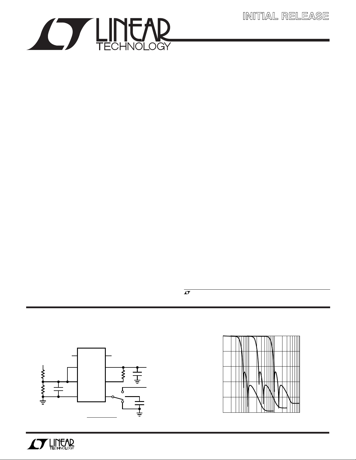
TYPICAL APPLICATIO
Single 3V Supply, 64kHz/16kHz/4kHz Lowpass Filter
18
+
IN
IN
3V
3.48k
2k
27
–
IN
LTC1569-6
36
GND
1µF
45
–
V
EASY TO SET f
CUTOFF
64kHz (10k/R
=
f
U
Frequency Response, f
0
OUTV
V
OUT
= 10k
R
EXT
+
V
R
X
1/16
EXT
1/4
1/1
)
DIV/CLK
:
CUTOFF
1, 4 OR 16
Information furnished by Linear Technology Corporation is believed to be accurate and reliable.
However, no responsibility is assumed for its use. Linear Technology Corporation makes no representation that the interconnection of its circuits as described herein will not infringe on existing patent rights.
3V
1µF
3V
100pF
1569-6 TA01
–20
–40
GAIN (dB)
–60
–80
–100
1
= 64kHz/16kHz/4kHz
CUTOFF
10 100 1000
FREQUENCY (kHz)
1569-6 TA01a
1
LTC1569-6
1
2
3
4
8
7
6
5
TOP VIEW
OUT
V
+
R
X
DIV/CLK
IN
+
IN
–
GND
V
–
S8 PACKAGE
8-LEAD PLASTIC SO
WU
A
W
O
LUTEXI TIS
S
A
WUW
ARB
U
G
PACKAGE
/
O
RDER I FOR ATIO
(Note 1)
Total Supply Voltage................................................ 11V
Power Dissipation.............................................. 500mW
Operating Temperature ................................ 0°C to 70°C
ORDER PART
NUMBER
LTC1569CS8-6
Storage Temperature ............................ –65°C to 150°C
Lead Temperature (Soldering, 10 sec).................. 300°C
S8 PART
MARKING
T
= 125°C, θJA = 150°C/W
JMAX
Consult factory for Industrial and Military grade parts.
LECTRICAL C CHARA TERIST
E
ICS
The ● denotes the specifications which apply over the full operating temperature range, otherwise specifications are at TA = 25°C.
VS = 3V (V+ = 3V, V– = 0V), f
PARAMETER CONDITIONS MIN TYP MAX UNITS
Filter Gain VS = 5V, f
Filter Phase VS = 2.7V, f
Filter Cutoff Accuracy R
when Self-Clocked V
Filter Output DC Swing VS = 3V, Pin 3 = 1.11V 2.1 V
(Note 6) ● 1.9 V
2
= 64kHz, R
CUTOFF
= 4.096MHz, fIN = 1280Hz = 0.02 • f
CLK
= 64kHz, VIN = 1.4V
f
CUTOFF
= 10k, Pin 5 Shorted to Pin 4 fIN = 32kHz = 0.5 • f
R
EXT
VS = 2.7V, f
f
CUTOFF
Pin 6 Shorted to Pin 4, External Clock f
f
CUTOFF
Pin 4, External Clock f
= 10.24k from Pin 6 to Pin 7, 62.5kHz ±1%
EXT
= 3V, Pin 5 Shorted to Pin 4
S
VS = 5V, Pin 3 = 2V 3.6 V
VS = ±5V, Pin 5 Shorted to Pin 7, R
= 1MHz, fIN = 312Hz = 0.02 • f
CLK
= 15.625kHz, VIN = 1V
= 4MHz, fIN = 1250Hz = 0.02 • f
CLK
= 62.5kHz, Pin 6 Shorted to fIN = 12.5kHz = 0.2 • f
= 10k unless otherwise specified.
LOAD
,f
P-P
,f
P-P
LOAD
= 12.8kHz = 0.2 • f
IN
f
= 51.2kHz = 0.8 • f
IN
= 64kHz = f
f
IN
= 97.5kHz = 1.5 • f
f
IN
f
= 128kHz = 2 • f
IN
= 192kHz = 3 • f
f
IN
= 3125kHz = 0.2 • f
IN
= 7812kHz = 0.5 • f
IN
= 12.5kHz = 0.8 • f
f
IN
= 15.625kHz = f
f
IN
f
= 23.44kHz = 1.5 • f
IN
= 31.25kHz = 2 • f
f
IN
= 46.88kHz = 3 • f
f
IN
= 31.25kHz = 0.5 • f
IN
= 50kHz = 0.8 • f
f
IN
f
= 62.5kHz = f
IN
= 93.75kHz = 1.5 • f
f
IN
= 20k 8.5 V
CUTOFF
CUTOFF
CUTOFF
CUTOFF
CUTOFF
CUTOFF
CUTOFF
CUTOFF
CUTOFF
CUTOFF
CUTOFF
CUTOFF
CUTOFF
CUTOFF
CUTOFF
CUTOFF
CUTOFF
CUTOFF
CUTOFF
CUTOFF
CUTOFF
CUTOFF
● –0.05 0.05 0.15 dB
● –0.25 –0.15 –0.05 dB
● –0.65 –0.55 –0.4 dB
● –1.3 –1.0 –0.7 dB
● –5.3 –3.8 –2.4 dB
● –60 –48 dB
● –62 –50 dB
● –71 –60 dB
● –0.12 0.05 0.16 dB
● –0.25 –0.15 –0.05 dB
● –0.65 –0.55 –0.4 dB
● –1.1 –0.9 –0.7 dB
● –3.6 –3.4 –3.2 dB
● –54 –50 dB
● –60 –55 dB
● –66 –60 dB
● – 114 –111 –108 Deg
● 79 82 85 Deg
● –83 –79 –75 Deg
● 156 162 168 Deg
● 3.2 V
15696
–11 Deg
–91 Deg
U
P-P
P-P
P-P
P-P
P-P
LTC1569-6
LECTRICAL C CHARA TERIST
E
The ● denotes the specifications which apply over the full operating temperature range, otherwise specifications are at TA = 25°C.
VS = 3V (V+ = 3V, V– = 0V), f
PARAMETER CONDITIONS MIN TYP MAX UNITS
Output DC Offset R
(Note 2) V
Output DC Offset Drift R
Clock Pin Logic Thresholds VS = 3V Min Logical “1” 2.7 V
when Clocked Externally Max Logical “0” 0.5 V
Power Supply Current f
(Note 3) Pin 5 Open, ÷ 4), f
Clock Feedthrough Pin 5 Open 0.1 mV
Wideband Noise Noise BW = DC to 2 • f
THD fIN = 3kHz, 1.5V
Clock-to-Cutoff 64
Frequency Ratio
Max Clock Frequency VS = 3V 5 MHz
(Note 4) V
Min Clock Frequency VS = 3V, 5V, TA < 85°C 1.5 kHz
(Note 5) V
Input Frequency Range Aliased Components <–65dB 0.9 • f
Note 1: Absolute maximum ratings are those values beyond which the life
of a device may be impaired.
Note 2: DC offset is measured with respect to Pin 3.
Note 3: If the internal oscillator is used as the clock source and the divide-
by-4 or divide-by-16 mode is enabled, the supply current is reduced as
much as 40% relative to the divide-by-1 mode.
= 4.096MHz, f
CLK
= 10k, Pin 5 Shorted to Pin 7 VS = 3V ±2 ±5mV
EXT
= 10k, Pin 5 Shorted to Pin 7 VS = 3V 25 µV/°C
EXT
VS = 5V Min Logical “1” 4.0 V
VS = ±5V Min Logical “1” 4.0 V
= 256kHz (40k from Pin 6 to Pin 7, VS = 3V 3 4 mA
CLK
f
= 4.096MHz (10k from Pin 6 to Pin 7, VS = 3V 8 mA
CLK
Pin 5 Shorted to Pin 4, ÷ 1), f
P-P
= 5V 5 MHz
S
= ±5V 7 MHz
V
S
= ±5V 3kHz
S
ICS
= 64kHz, R
CUTOFF
= 4kHz ● 5mA
CUTOFF
= 64kHz ● 11 mA
CUTOFF
CUTOFF
, f
= 32kHz 80 dB
CUTOFF
= 10k unless otherwise specified.
LOAD
= 5V ±6 ±12 mV
S
= ±5V ±15 mV
V
S
= 5V 25 µV/°C
V
S
V
= ±5V 75 µV/°C
S
Max Logical “0” 0.5 V
Max Logical “0” 0.5 V
VS = 5V 3.5 5 mA
● 6mA
VS = 10V 4.5 7 mA
● 8mA
V
= 5V 9 mA
S
VS = 10V 12 mA
Note 4: The maximum clock frequency is arbitrarily defined as the
frequency at which the filter AC response exhibits >1dB of gain peaking.
Note 5: The minimum clock frequency is arbitrarily defined as the frequecy
at which the filter DC offset changes by more than 5mV.
Note 6: For more details refer to the Input and Output Voltage Range
paragraph in the Applications Information section.
● 13 mA
● 17 mA
95 µV
CLK
RMS
RMS
Hz
3
LTC1569-6
UW
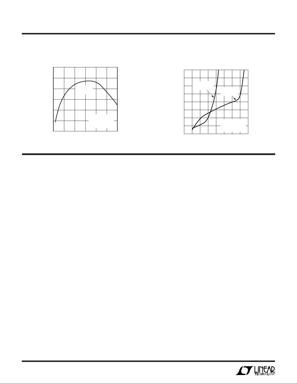
TYPICAL PERFOR A CE CHARACTERISTICS
–60
–65
–70
–75
THD (dB)
–80
–85
–90
0
VS = 5V
PIN 3 = 2V
VIN = 1.5V
P-P
f
= 32kHz
CUTOFF
+
IN
TO OUT
5 10 15 20 25 30
INPUT FREQUENCY (kHz)
1569-6 G01
THD (dB)
UUU
PIN FUNCTIONS
THD vs Input VoltageTHD vs Input Frequency
–50
–55
–60
–65
–70
–75
–80
–85
–90
VS = 3V
PIN 3 = 1.11V
0.5 1.0 1.5 2.0 2.5 3.0 3.5 4.0
0
INPUT VOLTAGE (V
VS = 5V
PIN 3 = 2V
fIN = 3kHz
f
CUTOFF
+
IN
TO OUT
)
P-P
= 32kHz
1569-6 G02
IN+/IN– (Pins 1, 2): Signals can be applied to either or
both input pins. The DC gain from IN+ (Pin 1) to OUT
(Pin␣ 8) is 1.0, and the DC gain from Pin 2 to Pin 8 is –1. The
input range, input resistance and output range are described in the Applications Information section. Input
voltages which exceed the power supply voltages should
be avoided. Transients will not cause latchup if the current
into/out of the input pins is limited to 20mA.
GND (Pin 3): The GND pin is the reference voltage for the
filter and should be externally biased to 2V (1.11V) to
maximize the dynamic range of the filter in applications
using a single 5V (3V) supply. For single supply operation,
the GND pin should be bypassed with a quality 1µF
ceramic capacitor to V– (Pin 4). The impedance of the
circuit biasing the GND pin should be less than 2kΩ as the
GND pin generates a small amount of AC and DC current.
For dual supply operation, connect Pin␣ 3 to a high quality
DC ground. A ground plane should be used. A poor ground
will increase DC offset, clock feedthrough, noise and
distortion.
+
V–/V
(Pins 4, 7): For 3V, 5V and ±5V applications a
quality 1µF ceramic bypass capacitor is required from V
+
(Pin 7) to V– (Pin 4) to provide the transient energy for the
internal clock drivers. The bypass should be as close as
possible to the IC. In dual supply applications (Pin 3 is
grounded), an additional 0.1µF bypass from V+ (Pin 7) to
GND (Pin 3) and V– (Pin 4) to GND (Pin 3) is recommended.
The maximum voltage difference between GND (Pin 3) and
V+ (Pin 7) should not exceed 5.5V.
DIV/CLK (Pin 5): DIV/CLK serves two functions. When the
internal oscillator is enabled, DIV/CLK can be used to
engage an internal divider. The internal divider is set to 1:1
when DIV/CLK is shorted to V– (Pin 4). The internal divider
is set to 4:1 when DIV/CLK is allowed to float (a 100pF
bypass to V– is recommended). The internal divider is set
to 16:1 when DIV/CLK is shorted to V+ (Pin 7). In the
divide-by-4 and divide-by-16 modes the power supply
current is reduced by as much as 40%.
When the internal oscillator is disabled (RX shorted
to V–) DIV/CLK becomes an input pin for applying an
external clock signal. For proper filter operation, the clock
waveform should be a squarewave with a duty cycle as
close as possible to 50% and CMOS voltages levels (see
Electrical Characteristics section for voltage levels). DIV/
CLK pin voltages which exceed the power supply voltages
should be avoided. Transients will not cause latchup if the
fault current into/out of the DIV/CLK pin is limited to 40mA.
4
 Loading...