

Linear Technology LTC1565-31 Datasheet

LTC1565-31
Final Electrical Specifications
650kHz Continuous Time,
Linear Phase Lowpass Filter
FEATURES
■
7th Order, 650kHz Linear Phase Filter in an SO-8
■
Differential Inputs and Outputs
■
Operates on a Single 5V or a ±5V Supply
■
Low Offset: 5mV Typical
■
75dB THD and SNR
■
78dB SNR
■
Shutdown Mode
■
Requires No External Components
■
Requires No External Clock Signal
U
APPLICATIO S
■
CDMA Base Stations
■
Data Communications
■
Antialiasing Filters
■
Smoothing or Reconstruction Filters
■
Matched Filter Pairs
■
Replacement for LC Filters
U
March 2000
DESCRIPTIO
The LTC®1565-31 is a 7th order, continuous time, linear
phase lowpass filter. The selectivity of the LTC1565-31,
combined with its linear phase and dynamic range, make it
suitable for filtering in data communications or data acquisition systems. The filter attenuation is 37dB at 2× f
and at least 72dB for frequencies above 3× f
CUTOFF
comparable LC filters, the LTC1565-31 achieves this selectivity with a linear phase response in the passband.
With 5% accuracy of the cutoff frequency, the LTC1565-31
can be used in applications requiring pairs of matched filters,
such as transceiver I and Q channels. Furthermore, the
differential inputs and outputs provide a simple interface for
these wireless systems.
With a single 5V supply and a 2V
input, the LTC1565-31
P-P
features an impressive spurious free dynamic range of 75dB.
The maximum signal-to-noise ratio is 78dB and it is achieved
with a 2.5V
input signal.
P-P
The LTC1565-31 features a shutdown mode where power
supply current is reduced to less than 10µA.
CUTOFF
. Unlike
U
TYPICAL APPLICATIO
Single 5V Supply, Differential 650kHz Lowpass Filter
0.1µF
1
+
V
IN
V
IN
+IN
2
–
–IN
LTC1565-31
3
GND
4
–
V
+OUT
–OUT
SHDN
8
7
6
+
V
5
V
OUT
V
OUT
5V
+
–
15645-31 TA01
0.1µF
Other cutoff frequencies and single-ended I/O can be provided upon request. Please contact LTC Marketing.
, LTC and LT are registered trademarks of Linear Technology Corporation.
Frequency Response
20
0
–20
5V
–40
–60
ATTENUATION (dB)
–80
–100
4
10
GAIN
GROUP DELAY
5
10
FREQUENCY (Hz)
6
10
1565-31 TA02
2.0
1.8
1.6
DELAY (µs)
1.4
1.2
1.0
0.8
7
10
Information furnished by Linear Technology Corporation is believed to be accurate and reliable.
However, no responsibility is assumed for its use. Linear Technology Corporation makes no representation that the interconnection of its circuits as described herein will not infringe on existing patent rights.
1
LTC1565-31
1
2
3
4
8
7
6
5
TOP VIEW
+OUT
–OUT
V
+
SHDN
+IN
–IN
GND
V
–
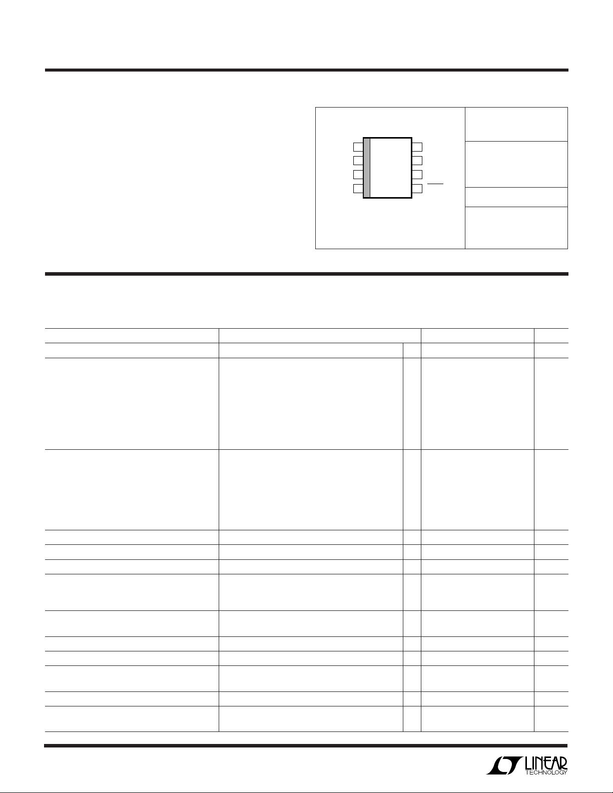
S8 PACKAGE
8-LEAD PLASTIC SO
WW
W
ABSOLUTE MAXIMUM RATINGS
U
U
W
PACKAGE/ORDER INFORMATION
U
(Note 1)
Total Supply Voltage............................................... 11V
Power Dissipation............................................. 500mW
Operating Temperature Range
LTC1565-31CS8 ..................................... 0°C to 70°C
LTC1565-31IS8 ................................. –40°C to 85°C
Storage Temperature Range ................ –65°C to 150°C
ORDER PART
NUMBER
LTC1565-31CS8
LTC1565-31IS8
S8 PART MARKING
Lead Temperature (Soldering, 10 sec)................. 300°C
T
= 150°C, θJA = 80°C/W (NOTE 5)
JMAX
Consult factory for Military grade parts.
ELECTRICAL CHARACTERISTICS
temperature range, otherwise specifications are at TA = 25°C. VS = 5V (V+ = 5V, V– = 0V), R
The ● denotes the specifications which apply over the full operating
= 10k from each output to AC ground,
LOAD
and Pin 5 open unless otherwise specified.
PARAMETER CONDITIONS MIN TYP MAX UNITS
Operating Supply Voltage 4.75 11 V
Filter Gain VIN = 1V
f
f
f
f
f
f
f
Filter Phase VIN = 1V
f
f
f
f
f
f
Phase Linearity Ratio of 600kHz Phase/300kHz Phase ● 1.97 2 2.03
Wideband Noise Noise BW = DC to 2 • f
THD fIN = 100kHz, 1V
Filter Differential DC Swing Maximum Difference Between Pins 7 and 8
V
VS = ±5V ● ±2.2 ±2.3 ±2.5 V
Filter DC Common Mode Range (Note 4) Upper V+ – 1.5 V
Lower V
Input Bias Current 0.1 0.3 0.6 µA
Input Offset Current 25 nA
Input Resistance Common Mode, VIN = 1.5V to 3.5V >50 MΩ
Differential >50 MΩ
Input Capacitance 2pF
Output DC Offset (Note 3) VS = 5V ±5 ±12 mV
2
V
S
, fIN = 25kHz ● –0.3 0 0.3 dB
P-P
= 200kHz (Gain Relative to 25kHz) ● –0.2 0 0.1 dB
IN
= 300kHz (Gain Relative to 25kHz) ● –0.7 –0.4 –0.1 dB
IN
= 500kHz (Gain Relative to 25kHz) ● –2.2 –1.6 –1.0 dB
IN
= 650kHz (Gain Relative to 25kHz) ● –4 –3 –2 dB
IN
= 900kHz (Gain Relative to 25kHz) ● –11 –7 dB
IN
= 1.3MHz (Gain Relative to 25kHz) ● –36 –31 dB
IN
= 2.3MHz (Gain Relative to 25kHz) –72 dB
IN
, fIN = 25kHz –13 Deg
P-P
= 200kHz –101 Deg
IN
= 300kHz ● –162 –150 –138 Deg
IN
= 500kHz 113 Deg
IN
= 600kHz ● 34 60 85 Deg
IN
= 650kHz 36 Deg
IN
= 900kHz –92 Deg
IN
CUTOFF
(Note 2) 85 dB
P-P
= 5V ● ±1.4 ±1.7 ±1.9 V
S
–
= ±5V (Note 6) ±5 ±12 mV
156531
56531I
115 µV
+ 0.8 V
RMS
P
P
LTC1565-31
ELECTRICAL CHARACTERISTICS
temperature range, otherwise specifications are at TA = 25°C. VS = 5V (V+ = 5V, V– = 0V), R
and Pin 5 open unless otherwise specified.
PARAMETER CONDITIONS MIN TYP MAX UNITS
Output DC Offset Drift VS = 5V –400 µV/°C
= ±5V –400 µV/°C
V
S
Ground Voltage (Pin 3) in VS = 5V ● 2.49 2.51 2.52 V
Single Supply Applications
SHDN Pin Logic Thresholds VS = 5V, Minimum Logical “1” 4.2 V
V
= 5V, Maximum Logical “0” 3.3 V
S
VS = ±5V, Minimum Logical “1” 2.75 V
= ±5V, Maximum Logical “0” 2.50 V
V
S
SHDN Pin Pull-Up Current VS = 5V 5 µA
= ±5V 9 µA
V
S
Power Supply Current VS = 5V ● 24 31 mA
= ±5V ● 25 33 mA
V
S
Power Supply Current in Shutdown Mode Shutdown. Includes SHDN Pull-Up Current
V
= 5V ● 4816 µA
S
= ±5V ● 10 20 40 µA
V
S
Note 1: Absolute Maximum Ratings are those values beyond which the life
of a device may be impaired.
Note 2: Input and output voltages expressed as peak-to-peak numbers are
assumed to be fully differential.
Note 3: Output DC offset is measured between Pin 8 and Pin 7 with Pin 1
and Pin 2 connected to Pin 3.
Note 4: A 250mV
The DC voltages at Pins 1 and 2 are equal. This is the “common mode
, 100kHz differential signal is applied to Pins 1 and 2.
P-P
The ● denotes the specifications which apply over the full operating
= 10k from each output to AC ground,
LOAD
voltage.” The “common mode range” is the range of common mode
voltages for which the 250mV
2nd or 3rd harmonic distortion.
Note 5: Thermal resistance varies depending upon the amount of PC board
metal attached to the device. θ
board covered with 2 oz copper on both sides.
Note 6: Output DC offset measurements are performed by automatic test
equipment approximately 0.5 seconds after application of power.
differential output has better than 65dB
P-P
is specified for a 3.8 square inch test
JA
UUU
PIN FUNCTIONS
+IN, –IN (Pins 1, 2): Input Pins. Signals can be applied to
either or both input pins. The DC gain from differential
inputs (Pin 1 to Pin 2) to the differential outputs (Pin 8 to
Pin 7) is 1.0V/V. The input range is described in the
Applications Information section.
GND (Pin 3): Ground. The ground pin is the reference
voltage for the filter and is internally biased to one-half the
total power supply voltage of the filter, maximizing the
dynamic range of the filter. For single supply operation,
the ground pin should be bypassed with a quality 0.1µF
ceramic capacitor to Pin 4. For dual supply operation,
connect Pin 3 to a high quality DC ground. A ground plane
should be used. A poor ground will increase noise and
distortion.
The impedance seen at Pin 3 is 2.5kΩ in normal mode. In
shutdown, the pin is internally biased to the same levels
as normal mode. The impedance in shutdown mode is
typically 500kΩ but varies with supply voltage and
temperature.
V–, V+ (Pins 4, 6): Power Supply Pins. For a single 5V
supply (Pin 4 grounded), a quality 0.1µF ceramic bypass
capacitor is required from the positive supply pin (Pin 6)
to the negative supply pin (Pin 4). The bypass should be as
close as possible to the IC. For dual supply applications
(Pin 3 is grounded), bypass Pin 6 to Pin 3 and Pin 4 to Pin
3 with a quality 0.1µF ceramic capacitor.
The maximum voltage difference between the ground pin
(Pin 3) and the positive supply pin (Pin 6) should not
exceed 5.5V.
3
 Loading...