

Linear Technology LTC1562-2 Datasheet
FEATURES
■
Continuous Time—No Clock
■
Four 2nd Order Filter Sections, 20kHz to 300kHz
Center Frequency
■
Butterworth, Chebyshev, Elliptic or Equiripple
Delay Response
■
Lowpass, Bandpass, Highpass Responses
■
99dB Typical S/N, ±5V Supply (Q = 1)
■
93dB Typical S/N, Single 5V Supply (Q = 1)
■
Rail-to-Rail Input and Output Voltages
■
DC Accurate to 3mV (Typ)
■
±0.5% Typical Center Frequency Accuracy
■
“Zero-Power” Shutdown Mode
■
Single or Dual Supply, 5V to 10V Total
■
Resistor-Programmable fO, Q, Gain
U
APPLICATIO S
■
High Resolution Systems (14 Bits to 18 Bits)
■
Antialiasing/Reconstruction Filters
■
Data Communications, Equalizers
■
Dual or I-and-Q Channels (Two Matched 4th Order
Filters in One Package)
■
Linear Phase Filtering
■
Replacing LC Filter Modules
LTC1562-2
Very Low Noise, Low Distortion
Active RC Quad Universal Filter
U
DESCRIPTIO
The LTC®1562-2 is a low noise, low distortion continuous
time filter with rail-to-rail inputs and outputs, optimized for a
center frequency (fO) of 20kHz to 300kHz. Unlike most
monolithic filters, no clock is needed. Four independent 2nd
order filter blocks can be cascaded in any combination, such
as one 8th order or two 4th order filters. Each block’s
response is programmed with three external resistors for
center frequency, Q and gain, using simple design formulas.
Each 2nd order block provides lowpass and bandpass outputs. Highpass response is available if an external capacitor
replaces one of the resistors. Allpass, notch and elliptic
responses can also be realized.
The LTC1562-2 is designed for applications where dynamic
range is important. For example, by cascading 2nd order
sections in pairs, the user can configure the IC as a dual 4th
order Butterworth lowpass filter with 90dB signal-to-noise
ratio from a single 5V power supply. Low level signals can
exploit the built-in gain capability of the LTC1562-2. Varying
the gain of a section can achieve a dynamic range as high as
114dB with a ±5V supply.
Other cutoff frequency ranges can be provided upon request.
Please contact LTC Marketing.
, LTC and LT are registered trademarks of Linear Technology Corporation.
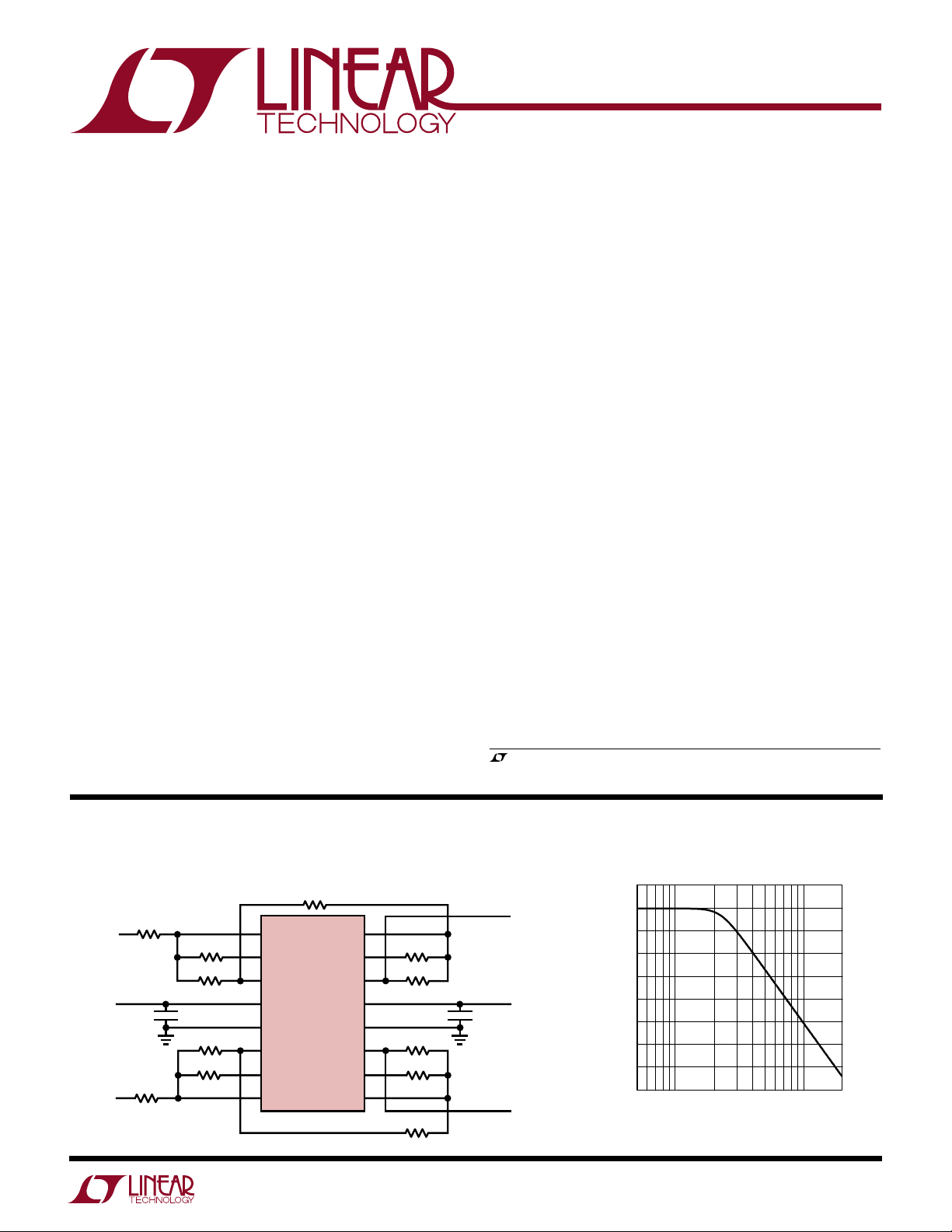
TYPICAL APPLICATIO
Dual 4th Order 200kHz Butterworth Lowpass Filter, SNR 96dB
R
7.87k
IN1
V
IN1
5V
R
IN3
V
IN2
*V– ALSO AT PINS 4, 7, 14 & 17
ALL RESISTORS 1% METAL FILM
7.87k
RQ1 4.22k
R21 7.87k
0.1µF
R23 7.87k
R
4.22k
Q3
1
INV B
2
V1 B
3
V2 B
5
+
LTC1562-2
V
6
SHDN
8
V2 A
9
V1 A
10
INV A
U
Amplitude Response
R
7.87k
IN2
V
0.1µF
OUT1
–5V*
V
OUT2
INV C
V1 C
V2 C
AGND
V2 D
V1 D
INV D
20
10.2k
R
Q2
19
R22 7.87k
18
16
–
V
15
R24 7.87k
13
10.2k
R
Q4
12
11
R
7.87k
IN4
1562-2 TA01
10
0
–10
–20
–30
–40
GAIN (dB)
–50
–60
–70
–80
50k
100k
1.5M1M
FREQUENCY (Hz)
1562-2 TA02
1
LTC1562-2
WW
W
U
ABSOLUTE MAXIMUM RATINGS
(Note 1)
Total Supply Voltage (V+ to V–) .............................. 11V
Maximum Input Voltage
at Any Pin ....................(V– – 0.3V) ≤ V ≤ (V+ + 0.3V)
Storage Temperature Range ................. –65°C to 150°C
Operating Temperature Range
LTC1562C-2 ............................................ 0°C to 70°C
LTC1562I-2 ........................................ –40°C to 85°C
Lead Temperature (Soldering, 10 sec).................. 300°C
ELECTRICAL CHARACTERISTICS
range, otherwise specifications are at T
specs are for a single 2nd order section, R
= 25°C. VS = ±5V, outputs unloaded, SHDN pin to logic “low”, unless otherwise noted. AC
A
= R2 = 10.4k ±0.1%, RQ = 9.09k ±0.1%, f
IN
The ● denotes specifications that apply over the full operating temperature
U
W
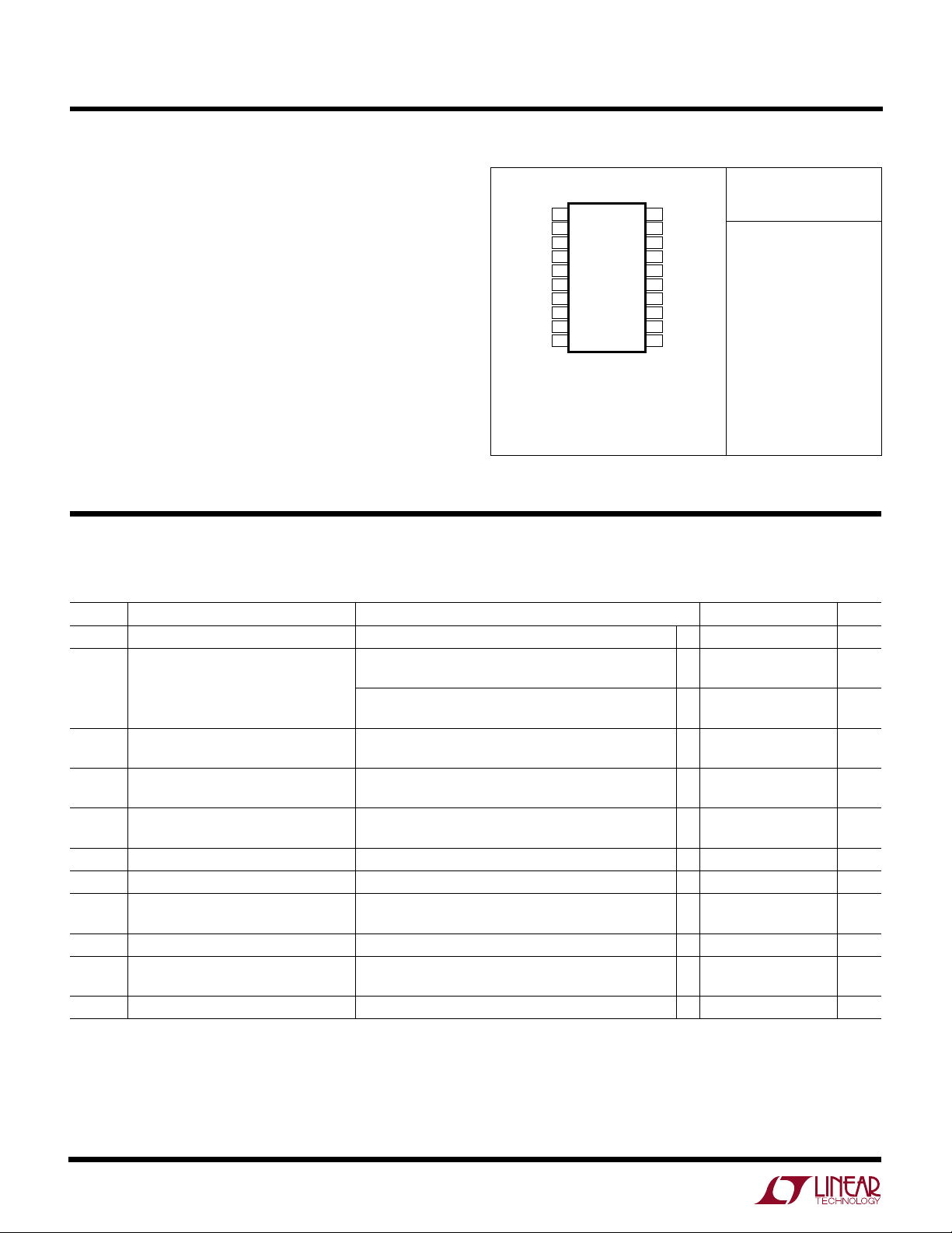
PACKAGE/ORDER INFORMATION
TOP VIEW
INV B
1
V1 B
2
V2 B
3
–*
V
4
+
V
5
SHDN
6
–*
V
7
V2 A
8
V1 A
9
INV A
10
G PACKAGE
20-LEAD PLASTIC SSOP
*G PACKAGE PINS 4, 7, 14, 17 ARE
SUBSTRATE/SHIELD CONNECTIONS
AND MUST BE TIED TO V
T
= 150°C, θJA = 136°C/W
JMAX
Consult factory for Military grade parts.
= 175kHz.
O
20
INV C
19
V1 C
18
V2 C
–*
17
V
–
16
V
15
AGND
–*
14
V
13
V2 D
12
V1 D
11
INV D
–
ORDER PART
NUMBER
LTC1562CG-2
LTC1562IG-2
U
SYMBOL PARAMETER CONDITIONS MIN TYP MAX UNITS
V
S
I
S
V
OS
H
L
Total Supply Voltage 4.75 10.5 V
Supply Current VS = ±2.375V, RL = 5k, CL = 30pF, Outputs at 0V 21 23.5 mA
= ±5V, RL = 5k, CL = 30pF, Outputs at 0V 22.5 25 mA
V
S
VS = ±2.375V, RL = 5k, CL = 30pF, Outputs at 0V ● 28 mA
V
= ±5V, RL = 5k, CL = 30pF, Outputs at 0V ● 30 mA
S
Output Voltage Swing, V2 Outputs VS = ±2.375V, RL = 5k, CL = 30pF ● 4.2 4.6 V
VS = ±5V, RL = 5k, CL = 30pF ● 9.3 9.8 V
Output Voltage Swing, V1 Outputs VS = ±2.375V, RL = 5k, CL = 30pF, f = 250kHz 4.5 V
VS = ±5V, RL = 5k, CL = 30pF, f = 250kHz 8.4 9.7 V
DC Offset Magnitude, V2 Outputs VS = ±2.375V, Input at AGND Voltage 3 17 mV
= ±5V, Input at AGND Voltage 3 17 mV
V
S
DC AGND Reference Point VS = Single 5V Supply 2.5 V
Center Frequency (fO) Error (Notes 2, 3) VS = ±5V, V2 Output Has RL = 5k, CL = 30pF 0.5 1.7 %
Lowpass Passband Gain at V2 Output VS = ±2.375V, fIN = 10kHz, ● 0 +0.05 +0.1 dB
V2 Output Has R
Q Accuracy VS = ±2.375V, V2 Output Has RL = 5k, CL = 30pF +2 %
Wideband Output Noise VS = ±2.375V, BW = 400kHz, Input AC GND 39 µV
VS = ±5V, BW = 400kHz, Input AC GND 39 µV
Input-Referred Noise, Gain = 100 BW = 400kHz, fO = 200kHz, Q = 1, Input AC GND 7.3 µV
= 5k, CL = 30pF
L
P-P
P-P
P-P
P-P
RMS
RMS
RMS
2
LTC1562-2
ELECTRICAL CHARACTERISTICS
range, otherwise specifications are at T
specs are for a single 2nd order section, R
= 25°C. VS = ±5V, outputs unloaded, SHDN pin to logic “low”, unless otherwise noted. AC
A
= R2 = 10.4k ±0.1%, RQ = 9.09k ±0.1%, f
IN
The ● denotes specifications that apply over the full operating temperature
= 175kHz.
O
SYMBOL PARAMETER CONDITIONS MIN TYP MAX UNITS
THD Total Harmonic Distortion, V2 Output fIN = 20kHz, 2.8V
R
= 5k, CL = 30pF
L
fIN = 20kHz, 9V
= 5k, CL = 30pF
R
L
Shutdown Supply Current SHDN Pin to V
SHDN Pin to V
, V1 and V2 Outputs Have –100 dB
P-P
, V1 and V2 Outputs Have – 82 dB
P-P
+
+
, VS = ±2.375V 1.0 µA
1.5 15 µA
Shutdown-Input Logic Threshold 2.5 V
Shutdown-Input Bias Current SHDN Pin to 0V –10 – 20 µA
Shutdown Delay SHDN Pin Steps from 0V to V
+
20 µs
Shutdown Recovery Delay SHDN Pin Steps from V+ to 0V 100 µs
Inverting Input Bias Current, Each Biquad 5 pA
Note 1: Absolute Maximum Ratings are those values beyond which the life
Note 3: Tighter frequency tolerance is available, consult factory.
of a device may be impaired.
Note 2: f
change from ±5V to ±2.375 supplies is – 0.2% typical,
O
temperature coefficient magnitude, 25°C to 85°C, is
f
O
50ppm/°C typical.
As with the LTC1562, fO decreases with increasing temperature.
UW
TYPICAL PERFOR A CE CHARACTERISTICS
fO Error vs Nominal fO (V
3.0
TA = 25°C
2.5
= R
R
IN
120
Q
160 200 240 280260140 180 220
NOMINAL fO (kHz)
2.0
1.5
1.0
0.5
0
–0.5
ERROR (%)
O
f
–1.0
–1.5
–2.0
–2.5
–3.0
= ±5V)
S
Q = 5
Q = 2.5
Q = 1
1562-2 G01
fO Error vs Nominal fO (V
3.0
TA = 25°C
2.5
= R
R
IN
120
Q
160 200 240 280260140 180 220
NOMINAL fO (kHz)
2.0
1.5
1.0
0.5
0
–0.5
ERROR (%)
O
f
–1.0
–1.5
–2.0
–2.5
–3.0
S
Q = 5
Q = 2.5
Q = 1
= ±2.5V)
1562-2 G02
Q Error vs Nominal fO (V
45
40
35
30
25
20
15
Q ERROR (%)
10
5
0
–5
100
TA = 70°C
= 25°C
T
A
= RQ
R
IN
140 180 220 300240120 160 200 280
NOMINAL fO (kHz)
= ±5V)
S
Q = 5
Q = 2.5
Q = 1
260
1562-2 G03
3
LTC1562-2
UW
TYPICAL PERFOR A CE CHARACTERISTICS
Q Error vs Nominal fO (V
55
50
45
40
35
30
25
20
Q ERROR (%)
15
10
5
0
–5
100
TA = 70°C
= 25°C
T
A
= RQ
R
IN
140 180 220 300240120 160 200 280
NOMINAL fO (kHz)
LP Noise vs Nominal f
(V
= ±5V, 25°C) (Figure 3,
S
V2 Output) (RIN = R2)
100
90
80
)
70
RMS
60
50
40
LP NOISE (µV
30
20
10
120
140 180
160
NOMINAL fO (kHz)
Q = 5
Q = 2.5
Q = 1
200
Q = 5
Q = 2.5
O
220
= ±2.5V)
S
Q = 1
260
240
1562-2 G04
260
1562-2 G07
280
Peak BP Gain vs Nominal f
(V
= ±5V) (Figure 3, V1 Output)
S
3.00
2.75
2.50
2.25
2.00
1.75
1.50
1.25
1.00
PEAK BP GAIN (dB)
0.75
0.50
0.25
0
100
TA = 70°C
T
R
= RQ
IN
120 160
140
BP Noise vs Nominal f
(V
= ±5V, 25°C) (Figure 3,
S
V1 Output) (RIN = RQ)
100
90
80
)
70
RMS
60
50
40
BP NOISE (µV
30
20
10
120
140 180
160
NOMINAL fO (kHz)
= 25°C
A
200 280
180
NOMINAL fO (kHz)
Q = 5
Q = 2.5
Q = 1
200
220
Q = 2.5
220
O
240
Q = 5
Q = 1
240
O
260
260
1562-2 G08
Peak BP Gain vs Nominal f
(V
= ±2.5V) (Figure 3, V1 Output)
S
1562-2 G5
300
4.00
3.75
3.50
3.25
3.00
2.75
2.50
2.25
2.00
1.75
1.50
1.25
PEAK BP GAIN (dB)
1.00
0.75
0.50
0.25
0
100
TA = 70°C
T
A
R
= RQ
IN
120 160
140
= 25°C
Distortion vs External Load
Resistance and Frequency
(V
= ±5V, 25°C) (Figure 8)
S
0
2nd ORDER LOWPASS
–10
= 200kHz
f
O
Q = 0.7
–20
OUTPUT LEVEL 1V
±5V SUPPLIES
–30
–40
–50
–60
–70
–80
–90
THD (AMPLITUDE BELOW FUNDAMENTAL) (dB)
–100
280
10k
EXTERNAL LOAD RESISTANCE (Ω)
RMS
fIN = 100kHz
f
= 50kHz
IN
= 20kHz
f
IN
5k
Q = 5
Q = 2.5
Q = 1
200 280
220
180
NOMINAL fO (kHz)
(2.83V
)
P-P
2k
240
1562-2 G09
260
O
300
1562-2 G6
THD (AMPLITUDE BELOW FUNDAMENTAL) (%)
100
10
1
0.1
0.01
0.001
1k
UUU
PIN FUNCTIONS
Power Supply Pins: The V+ and V– pins should be
bypassed with 0.1µF capacitors to an adequate analog
ground or ground plane. These capacitors should be
connected as closely as possible to the supply pins. Pins
4, 7, 14 and 17 are internally connected to V– (Pin 16) and
should also be tied to the same point as Pin 16 for best
shielding. Low noise linear supplies are recommended.
Switching supplies are not recommended as they will
lower the filter dynamic range.
4
Analog Ground (AGND): The AGND pin is the midpoint of
a resistive voltage divider, developing a potential halfway
between the V+ and V– pins, with an equivalent series
resistance nominally 7k. This serves as an internal ground
reference. Filter performance will reflect the quality of the
analog signal ground and an analog ground plane
surrounding the package is recommended. The analog
ground plane should be connected to any digital ground at
a single point. For dual supply operation, the AGND pin
UUU
PIN FUNCTIONS
LTC1562-2
should be connected to the ground plane (Figure 1). For
single supply operation, the AGND pin should be bypassed
to the ground plane with at least a 0.1µF capacitor (at least
1µF for best AC performance) (Figure 2).
ANALOG
GROUND
PLANE
+
V
0.1µF
SINGLE-POINT
SYSTEM GROUND
10
1
2
3
4
5
6
7
8
9
LTC1562-2
20
19
18
17
16
15
14
13
12
11
GROUND PLANE
DIGITAL
(IF ANY)
–
V
0.1µF
Shutdown (SHDN): When the SHDN input goes high or is
open-circuited, the LTC1562-2 enters a “zero-power”
shutdown state and only junction leakage currents flow.
The AGND pin and the amplifier outputs (see Figure 3)
assume a high impedance state and the amplifiers effectively disappear from the circuit. (If an input signal is
applied to a complete filter circuit while the LTC1562-2 is
in shutdown, some signal will normally flow to the output
through passive components around the inactive op amps.)
A small pull-up current source at the SHDN input
defaults
the LTC1562-2 to the shutdown state if the SHDN pin is left
floating
. Therefore, the user
must
connect the SHDN pin
to a logic “low” (0V for ±5V supplies, V– for 5V total
supply) for normal operation of the LTC1562-2. (This
convention permits true “zero-power” shutdown since not
even the driving logic must deliver current while the part
is in shutdown.) With a single supply voltage, use V– for
logic “low,” do not connect SHDN to the AGND pin.
1562-2 F01
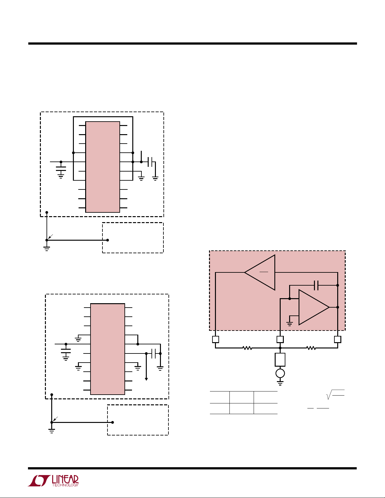
Figure 1. Dual Supply Ground Plane Connection
(Including Substrate Pins 4, 7, 14, 17)
ANALOG
GROUND
PLANE
+
V
0.1µF
SINGLE-POINT
SYSTEM GROUND
10
1
2
3
4
5
6
7
8
9
LTC1562-2
20
19
18
17
16
15
14
13
12
+
V
11
GROUND PLANE
/2
REFERENCE
DIGITAL
(IF ANY)
1µF
1562-2 F01
Figure 2. Single Supply Ground Plane Connection
(Including Substrate Pins 4, 7, 14, 17)
1/4 LTC1562-2
1
sR1C*
*R1 AND C ARE PRECISION
INTERNAL COMPONENTS
C
–
+
V2 V1
ZIN TYPE
R
C
R2
RESPONSE
AT V1
BANDPASS
HIGHPASS
RESPONSE
AT V2
LOWPASS
BANDPASS
INV
Z
IN
+
V
IN
–
R
Q
IN EACH CASE,
= (200kHz)
f
O
RQ
Q =
R2
7958Ω
()
R2
200kHz
()
f
O
1562-2 F03
Figure 3. Equivalent Circuit of a Single 2nd Order Section
(Inside Dashed Line) Shown in Typical Connection. Form of
ZIN Determines Response Types at the Two Outputs (See Table)
5
 Loading...