

Linear Technology LTC1560-1 Datasheet
LTC1560-1
FREQUENCY (MHz)
0.1
–90
GAIN (dB)
–70
–50
–30
–10
110
1560-1 TA02
10
–80
–60
–40
–20
0
f
CUTOFF
= 1MHz/500kHz
1MHz/500kHz
Continuous Time,
Low Noise, Lowpass Elliptic Filter
FEATURES
■
5th Order, 1MHz Elliptic Filter in SO-8 Package
■
Pin Selectable 1MHz/500kHz Cutoff Frequency
■
Signal-to-Noise Ratio (SNR): 75dB
■
Signal-to-Noise Ratio with –63dB THD: 69dB
■
Passband Ripple (f
■
Stopband Attenuation Better Than 60dB
■
No External Components Required
= 1MHz): ±0.3dB
CUTOFF
U
APPLICATIONS
■
Antialiasing Filters
■
Smoothing or Reconstruction Filters
■
Communication Filters
U
DESCRIPTION
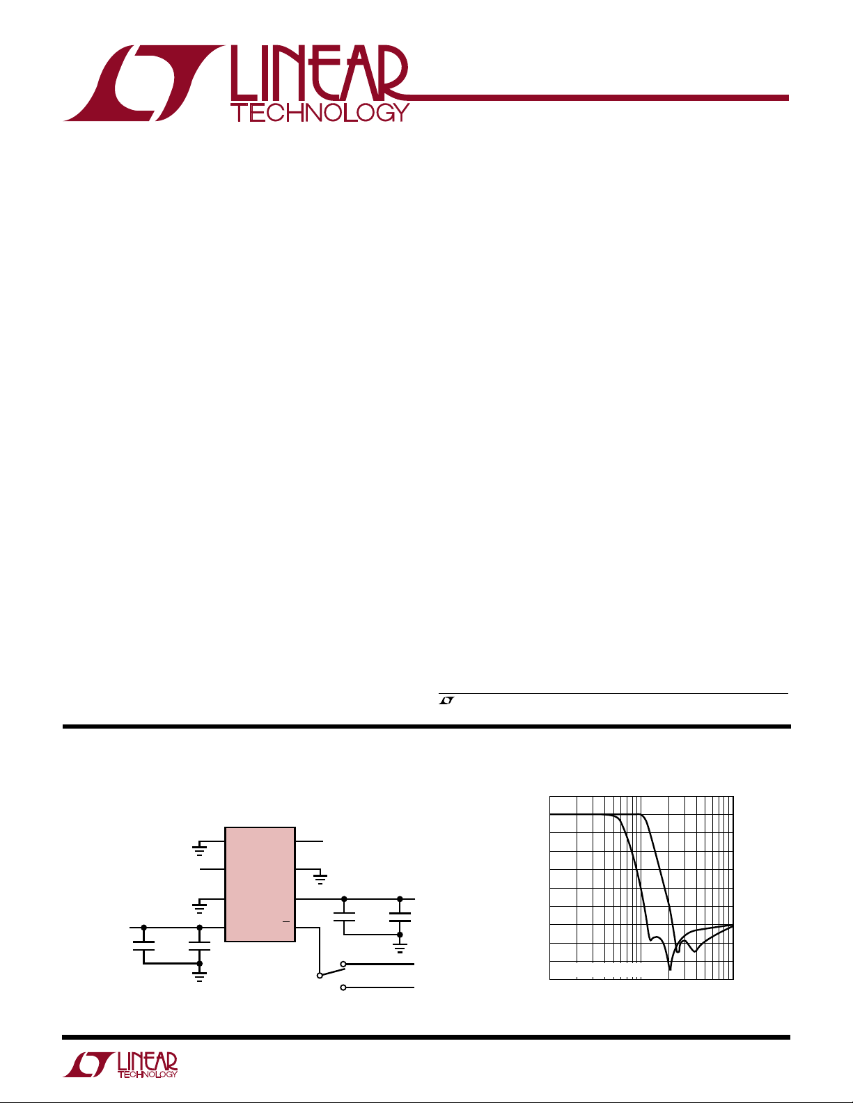
The LTC®1560-1 is a 5th order, continuous-time, lowpass
filter.
The elliptic transfer function of the LTC1560-1 was
carefully chosen to reach a compromise between selectivity, for antialiasing applications, and transient response.
The filter cutoff frequency, f
, is pin selectable to
CUTOFF
either 500kHz (Pin 5 to V+) or 1MHz (Pin 5 to V–). When
programmed for 1MHz, the passband ripple is typically
± 0.2dB up to 0.55f
transition band gain is –24dB at 1.4f
2f
. Stopband attenuation is 63dB at 2.43f
CUTOFF
and ±0.3dB to 0.9f
CUTOFF
CUTOFF
. The
CUTOFF
and –51dB at
and
CUTOFF
above, remaining at least 60dB to 10MHz with proper
board layout. When the LTC1560-1 is programmed for
f
= 500kHz, the filter response closely follows the
CUTOFF
1MHz case with the exception of passband flatness near
the cutoff frequency; the gain at f
CUTOFF
is –1.3dB.
The LTC1560-1, unlike other high frequency filters, is
designed for low noise and low distortion. With a 1V
RMS
input signal, the signal-to-noise ratio is 69dB and the THD
is –63dB. The maximum SNR of 75dB is obtained with a
2.1V
input signal. This results in –46dB THD.
RMS
The LTC1560-1 operates with ±5V supplies, has a power
saving mode and is available in an SO-8 surface mount
package.
Other cutoff frequencies from 450kHz to 1.5MHz can be
obtained. Demo board DC135A is available for the
LTC1560-1. For more information please contact LTC
Marketing.
, LTC and LT are registered trademarks of Linear Technology Corporation.
TYPICAL APPLICATION
1MHz/500kHz Elliptic Lowpass Filter
1
GND
2
V
3
GND
4
V
–5V
0.1µF
V
IN
0.01µF
IN
LTC1560-1
–
0.5f
V
OUT
SHDN
V
C/fC
U
Frequency Response
8
V
OUT
7
(OR –5V)
6
+
5
0.1µF
5V
0.01µF
–5V
1MHz
5V
500kHz
1560-1 TA01
1
LTC1560-1
WW
W
ABSOLUTE MAXIMUM RATINGS
Total Supply Voltage (V+ to V–) ............................. 12V
Power Dissipation............................................. 400mW
Burn-In Voltage ................................................... ±5.5V
Operating Temperature Range
LTC1560-1C ........................................... 0°C to 70°C
LTC1560-1I ....................................... –40°C to 85°C
Maximum Junction Temperature ......................... 150°C
Storage Temperature Range ................. – 65°C to 150°C
Lead Temperature (Soldering, 10 sec).................. 300°C
U
U
W
PACKAGE/ORDER INFORMATION
TOP VIEW
GND
1
V
2
IN
GND
3
–
V
4
S8 PACKAGE
8-LEAD PLASTIC SO
T
= 150°C, θJA = 125°C/ W
JMAX
Consult factory for Military grade parts.
V
8
OUT
SHDN
7
+
V
6
0.5fC/f
5
C
ORDER PART
NUMBER
LTC1560-1CS8
LTC1560-1IS8
S8 PART MARKING
15601
15601I
U
ELECTRICAL CHARACTERISTICS
VS = ±5V, TA = 25°C, Pin 5 = –5V (f
PARAMETER CONDITIONS MIN TYP MAX UNITS
Operating Supply Voltage Range ±4.5 ±5.0 ±5.5 V
Passband Gain (f
Transition Band Gain (Note 1) VIN = 0.5V
Stopband Gain (f
Passband Gain (f
Output Voltage Swing RL = 5k ● ±1.9 ±3V
Output DC Offset (VOS) ±250 mV
Power Supply Current (IS) ● 22 29 mA
Power Supply Current in Shutdown Mode Pin 7 at 5V 1 mA
Total Output Noise VIN (Pin 2) Tied to Ground, f
Total Harmonic Distortion (THD) VIN = 1V
Input Resistance (RIN) ● 6 8 10 kΩ
= 1MHz) VIN = 0.5V
CUTOFF
= 1MHz) (Note 2) fIN = 2.44MHz ● –70 –65 dB
CUTOFF
= 500kHz) fIN = 100kHz, Pin 5 = 5V 0.14 dB
CUTOFF
= 1MHz), Pin 7 = 0V unless otherwise specified.
CUTOFF
= 20kHz 0.17 dB
RMS,fIN
f
= 100kHz ● –0.3 0.18 0.6 dB
IN
f
= 300kHz 0.08 dB
IN
f
= 550kHz (Gain Relative to 100kHz) ● –0.35 0.05 0.3 dB
IN
= 850kHz (Gain Relative to 100kHz) ● –0.8 –0.3 0 dB
f
IN
f
= 950kHz (Gain Relative to 100kHz) ● –3.0 0.6 0.5 dB
IN
f
= f
IN
= 1.4MHz ● –24 –18 dB
RMS,fIN
f
= 1.9MHz –42 dB
IN
f
= 2.0MHz –51 dB
IN
f
= 3.0MHz –68 dB
IN
f
= 6.0MHz –66.1 dB
IN
f
= f
IN
f
= 1.4MHz –45 dB
IN
VIN (Pin 2) Tied to Ground, f
, fIN = 200kHz, f
RMS
f
= 300kHz, f
IN
= 1MHz, f
f
IN
fIN = 300kHz, f
f
= 500kHz, f
IN
= 1MHz (Gain Relative to 100kHz) ● –5.0 – 1.0 1.0 dB
CUTOFF
= 500kHz ● –4 –1.6 0.5 dB
CUTOFF
= 1MHz, BW = 2MHz 350 µV
CUTOFF
= 0.5MHz, BW = 1MHz 322 µV
CUTOFF
= 1MHz, BW = 1MHz –63 dB
CUTOFF
= 1MHz, BW = 1MHz –61 dB
CUTOFF
= 1MHz, BW = 2MHz –62 dB
CUTOFF
= 0.5MHz, BW = 1MHz –62 dB
CUTOFF
= 0.5MHz, BW = 1MHz –63 dB
CUTOFF
RMS
RMS
The ● denotes specifications which apply over the full operating
temperature range.
Note 1: To properly measure high frequency characteristics of the filter, a
noninverting output buffer is recommended as shown on the demo board
2
connection diagram, Figure 2. A small resistor (e.g. 100Ω) can also be
used instead of the buffer to isolate any high capacitive load (C
from the filter output.
Note 2: The stopband gain at 2.44MHz is guaranteed by design.
> 10pF)
L
FREQUENCY (MHz)
0.1
GAIN (dB)
0
0.2
0.4
0.6
0.5
1560-1 G03
–0.2
–0.4
–0.6
0.2
0.3
0.4
0.6 0.7 0.8 0.9 1.0
f
CUTOFF
= 1MHz
W
U
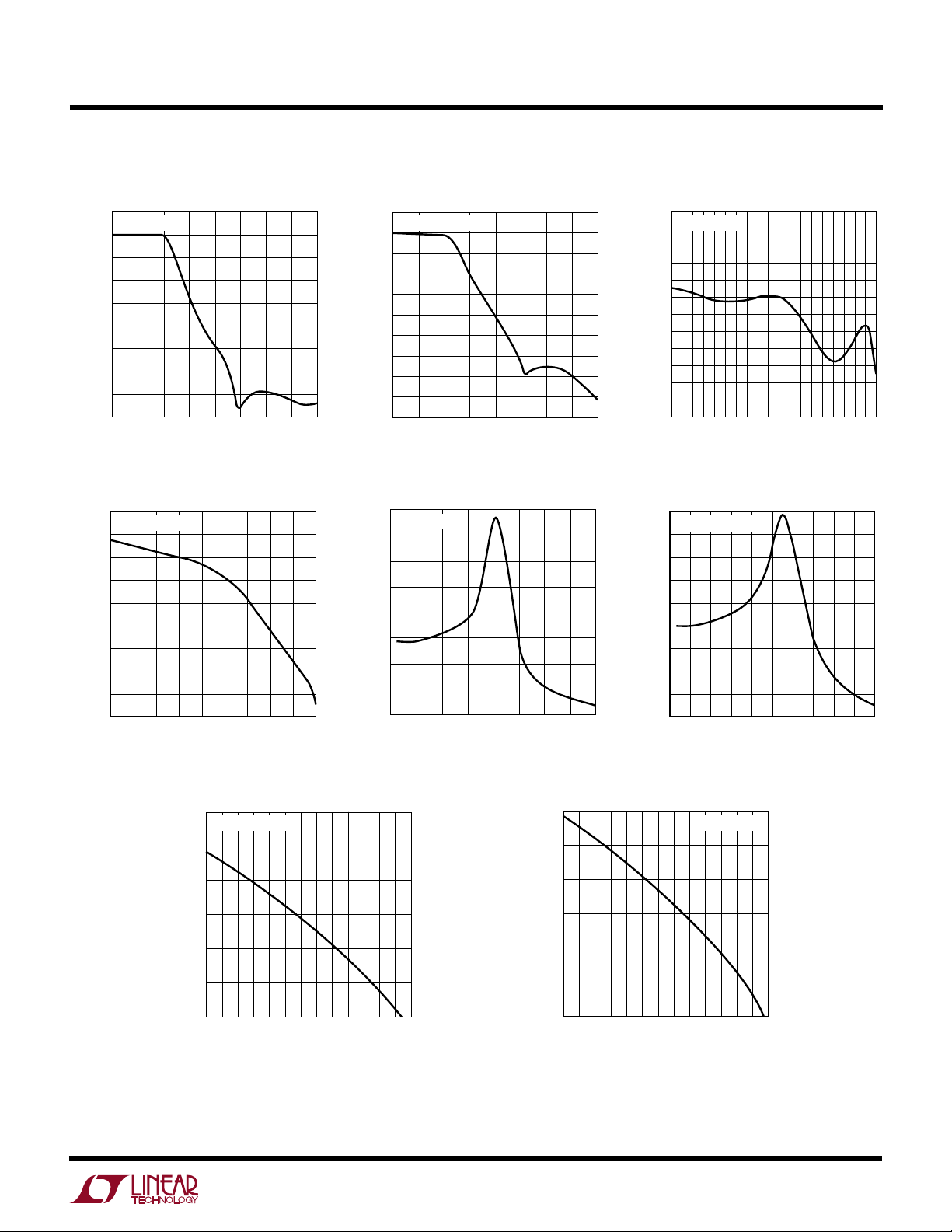
TYPICAL PERFORMANCE CHARACTERISTICS
LTC1560-1
Frequency Response
10
f
= 1MHz
CUTOFF
0
–10
–20
–30
–40
GAIN (dB)
–50
–60
–70
–80
0.4
0.2
0
–0.2
–0.4
–0.6
GAIN (dB)
–0.8
–1.0
–1.2
–1.4
0
f
CUTOFF
1
= 500kHz
2
FREQUENCY (MHz)
0.20.1 0.5
FREQUENCY (MHz)
3
1560-1 G01
0.3 0.4
1560-1 G04
Frequency Response Passband Gain
10
f
= 500kHz
CUTOFF
0
–10
–20
–30
–40
GAIN (dB)
–50
–60
–70
–80
4
–90
0
Group Delay
1.6
f
CUTOFF
1.4
1.2
1.0
0.8
0.6
GROUP DELAY (µs)
0.4
0.2
0
0
0.25
= 1MHz
0.50
0.5
1.0
FREQUENCY (MHz)
1.0
0.75
FREQUENCY (MHz)
1.25
1.5
1.50
1560-1 G02
1.75
1560-1 G05
2.0
2.0
GROUP DELAY (µs)
2.25
2.00
1.75
1.50
1.25
1.00
0.75
0.50
0.25
Group DelayPassband Gain
0
0
f
= 500kHz
CUTOFF
0.1 0.3
0.2 0.4 0.5 0.6 0.7 0.8 0.9 1.0
FREQUENCY (MHz)
1560-1 G06
Phase vs Frequency
45
f
CUTOFF
0
–45
–90
PHASE (DEG)
–135
–180
–225
20
= 500kHz
180
FREQUENCY (kHz)
Phase vs Frequency
0
–45
–90
–135
PHASE (DEG)
–180
–225
–270
260100
340
500420
1560-1 G07
20
180
340
FREQUENCY (kHz)
f
= 1MHz
CUTOFF
500 660 820 980
1560-1 G08
3
 Loading...