

Linear Technology LTC1559-5, LTC1559-3.3 Datasheet
1
LTC1559-3.3/LTC1559-5
Backup Battery Controller
with Fixed Output
■
Complete Battery Backup System in an SO-8,
16-Pin GN or SO Package
■
Generates Fixed Backup Voltage (3.07V/4.63V) from
a Single 1.2V NiCd Button Cell
■
Automatic Main Supply to Backup Switching
■
Minimum 100mW Output Power
■
Automatic Fast Recharge of NiCd Battery
■
Programmable NiCd Trickle Charge Current
■
Smart NiCd Charger Minimizes Recharge Time and
Maximizes System Efficiency After Backup
■
Onboard Power-Up and Push-Button Reset
Generator
■
Performs VCC Supervisory Functions
■
Reset Assertion Guaranteed at VCC = 1V
■
Short-Circuit Protection
■
Thermal Limiting
FEATURES
DESCRIPTION
U
The LTC®1559 is a backup battery controller that provides
all the functions necessary to implement a backup 3.3V or
5V power supply using a single NiCd cell. It includes a 1.2V
to 3.07V/4.63V boost converter, an intelligent 2-stage
battery charger, automatic backup switching and a microprocessor reset generator. The boost converter uses a
synchronous switching architecture to achieve a typical
efficiency of 70%, ensuring maximum backup lifetime
from a small NiCd cell.
The on-chip NiCd charger uses an internal gas gauge to
minimize fast recharge time and prevent overcharging of
the backup cell, thereby improving system efficiency and
extending the life of the backup cell. The LTC1559 also
provides a user programmable trickle charge current to
compensate for self-discharge losses in the backup cell.
The LTC1559’s automatic backup switching scheme
requires minimum intervention from the host system and
provides feedback to the host to minimize system loading
in the backup state. Its internal VCC fault detector and reset
generator eliminate the need for a separate microprocessor supervisory chip in most applications.
The LTC1559 is available in an SO-8, 16-pin GN or SO
package.
APPLICATIONS
U
■
Notebook Computers
■
Palmtop Computers/PDAs
■
Portable Instruments
■
Battery-Powered Systems
, LTC and LT are registered trademarks of Linear Technology Corporation.
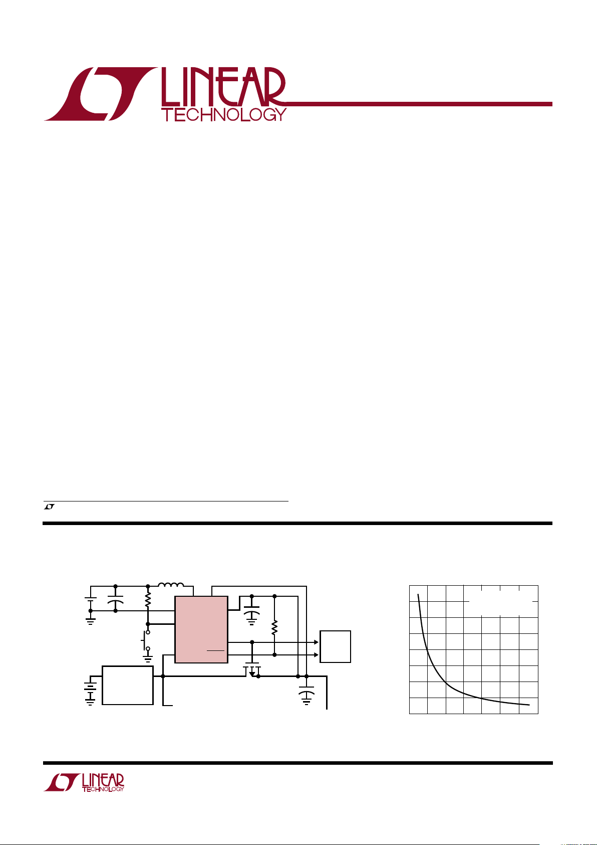
TYPICAL APPLICATION
U
CTL
C1
1µF
**BACKUP
BATTERY
1.2V
NiCd
MAIN
BATTERY
4.5V TO 28V
R1
68k
SW
LTC1559-3.3
*L1
22µH
GND
PS
7
1
8
5
6
3
S1
RESET
1559 TA01
2
4
V
BAK
V
CC
RESET
BACKUP
+
C3
100µF
10V
V
OUT
3.3V AT NORMAL MODE
3A
V
BAK
33mA (3.07V) AT BACKUP MODE
>33mA (3.3V) AT NORMAL MODE
C2
1µF
SYSTEM
µP
R2
100k
Q1
P-MOSFET
Si9424DY
* SUMIDA CD54-22µH
** PANASONIC P-11AAH
† CONSULT LTC1435 DATA SHEET FOR
APPLICATION CIRCUIT INFORMATION
†
LTC1435
SYNCHRONOUS
BUCK
REGULATOR
+
+
Backup Time vs
V
BAK
Output Load Current
V
BAK
LOAD CURRENT (mA)
0
BACKUP TIME (MINUTES)
800
700
600
500
400
300
200
100
0
15 25
1559 TA02
510
20 30 35
V
BAK
= 3.07V
NiCd CELL = P-11AAH
(110mA Hrs)
2
LTC1559-3.3/LTC1559-5
ABSOLUTE MAXIMUM RATINGS
W
WW
U
(Note 1)
Terminal Voltages
VCC........................................................................ 6V
V
BAK
.................................................................... 12V
SW ...................................................................... 14V
All Other Pins .............................. – 0.3V to VCC + 0.3V
SW Input Currents ............................................. 500mA
V
BAK
Output Current ................... Short-Circuit Protected
Operating Ambient Temperature Range ....... 0°C to 70°C
Junction Temperature .......................................... 125°C
Storage Temperature Range .................. –65°C to 150°C
Lead Temperature (Soldering, 10 sec)...................300°C
ORDER PART
NUMBER
ORDER PART
NUMBER
S8 PART MARKING
LTC1559CS8-3.3
LTC1559CS8-5
ELECTRICAL CHARACTERISTICS
V
BAT
= 1.2V, TA = 0°C to 70°C unless otherwise noted.
LTC1559CGN-3.3
LTC1559CGN-5
LTC1559CS-3.3
LTC1559CS-5
Consult factory for Industrial and Military grade parts.
T
JMAX
= 125°C, θJA = 130°C/ W
1
2
3
4
8
7
6
5
TOP VIEW
S8 PACKAGE
8-LEAD PLASTIC SO
SW
GND
CTL
PS
V
BAK
V
CC
BACKUP
RESET
T
JMAX
= 125°C, θJA = 110°C/ W (GN)
T
JMAX
= 125°C, θJA = 110°C/ W (S)
TOP VIEW
S PACKAGE
16-LEAD PLASTIC SO
GN PACKAGE
16-LEAD PLASTIC SSOP
1
2
3
4
5
6
7
8
16
15
14
13
12
11
10
9
SW
SW
PGND
GND
CTL
SHDN
PS
NC
V
BAK
V
BAK
V
CC
BACKUP
RESET
RESET
NC
LOBAT
PACKAGE/ORDER INFORMATION
W
U
U
SYMBOL PARAMETER CONDITIONS MIN TYP MAX UNITS
Battery Backup Switching
V
CC
Operating Voltage Range LTC1559-3.3 ● 2.900 3.5 V
LTC1559-5 ● 4.400 5.5 V
V
BAT
Backup Battery Cell Voltage ● 1.0 1.2 1.5 V
I
VCC
Quiescent Supply Current (Note 2) ● 155 250 µA
I
BAT
Peak Inductor Current (Backup) Boost Converter in Low Current Mode (Note 7) ● 80 165 225 mA
Boost Converter in High Current Mode (Note 7) ● 225 330 445 mA
I
BAT(SHDN)
Battery Standby Current VCC = 0V ● 0.1 15 µA
I
VCC(SHDN)
Supply Current During Shutdown (Note 3) ● 50 µA
V
BAK(ON)VCC
Backup Request/Booster Assertion LTC1559-3.3 ● 3.011 3.070 3.127 V
Trip Point (Note 4) LTC1559-5 ● 4.475 4.625 4.775 V
V
BAK(OFF)VCC
Backup Deassertion Trip Point LTC1559-3.3 ● 3.061 3.119 3.176 V
(Note 4) LTC1559-5 ● 4.550 4.700 4.850 V
V
LOBAT1
Low V
BAT
Detect (Note 3) ● 0.95 1.00 1.05 V
V
UVLO(ON)VCC
UVLO Trip Voltage (Note 4) LTC1559-3.3 ● 2.904 3.003 3.102 V
LTC1559-5 ● 4.400 4.550 4.700 V
V
UVLO(OFF)VCC
UVLO Trip Voltage (Note 4) LTC1559-3.3 ● 3.061 3.119 3.176 V
LTC1559-5
● 4.550 4.700 4.850 V
155933
15595
3
LTC1559-3.3/LTC1559-5
ELECTRICAL CHARACTERISTICS
V
BAT
= 1.2V, TA = 0°C to 70°C unless otherwise noted.
SYMBOL PARAMETER CONDITIONS MIN TYP MAX UNITS
UVLO Reset Monitor
V
LOBAT2VBAT
UVLO Trip Voltage (Note 5) ● 0.85 0.9 0.95 V
Backup Battery Charger
I
CHGF
Battery Charge Current During Fast Recharge ● 11 16 21 mA
I
CHGT
User-Programmable Trickle Charge ● 0.05 2 mA
Current Range
Q
RECH
Fast Recharge Factor (Note 6) 1.35 1.6 1.85 C/C
Q
TRK
Nominal Trickle Charge Multiplier Factor I
CHGT
= 1mA ● 8 10 12 A/A
V
CTL(CLAMP)
CTL Clamp Voltage in Trickle Mode I
CHGT
= 1mA ● 0.45 0.5 0.55 V
Push-Button Reset
V
CTL
CTL Input Threshold 250 mV
t
CTL
CTL Input Low Time (Debounce Time) 20 26 ms
Reset Timer
t
HRESET
Push-Button Duration for Hard Reset 1.10 1.8 3.4 sec
t
RST
RESET Pulse Width V
CTL
Low for <t
HRESET
(Soft Reset) ● 50 80 150 µs
V
CTL
Low for >t
HRESET
(Hard Reset) ● 115 185 345 ms
V
RST1
RESET Output Voltage VCC = 1V, I
SINK
= 10µA ● 5 200 mV
V
RST
RESET Output Voltage VCC = 4.25V, I
SINK
= 1.6mA ● 0.1 0.4 V
I
SC
RESET Output Current Output Source Current VCC = 3.3V 10 mA
Output Source Current VCC = 5V 20 mA
Short-Circuit Current Output Sink Current VCC = 3.3V 20 mA
Output Sink Current V
CC
= 5V 40 mA
PS Comparator
V
HYST
Comparator Threshold Hysteresis TA = 25°C90mV
Internal VCC Monitor Comparator
tr UVLO, Comparator Propagation Delay (Rising) 7.5 µs
Shutdown Pin (Note 3)
V
SHDN
SHDN Input Threshold Logic Low, V
IL
● 0.8 V
Logic High, V
IH
● 2V
I
SHDN
SHDN Pin Bias Current VCC = 5V, V
SHDN
= 0V ● 815 µA
The ● denotes specifications which apply over the full operating
temperature range.
Note 1: Absolute Maximum Ratings are those values beyond which the life of
a device may be impaired.
Note 2: Quiescent current is measured during push-button reset.
Note 3: Only applies to 16-pin version.
Note 4: Although the V
BAK(ON)
, V
BAK(OFF)
, V
UVLO(ON)
and V
UVLO(OFF)
threshold voltages have a specification tolerance, they are guaranteed by
design and tested in production never to overlap.
Note 5: Low cell voltage reset is only triggered when 0.25V < V
CTL
< 0.9V
for at least 20µs while in backup mode.
Note 6: Fast recharge factor is defined as the ratio of charge replenished to
the NiCd battery during fast recharge to the charge withdrawn from the
NiCd battery during backup.
Note 7: The LTC1559 switches automatically between the low and high
operating current levels. See Applications Information for more details.
4
LTC1559-3.3/LTC1559-5
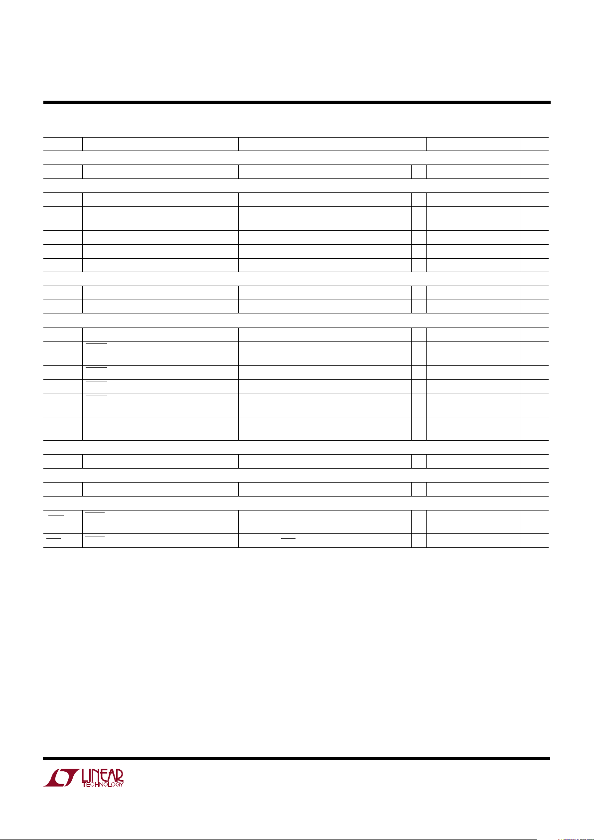
TYPICAL PERFORMANCE CHARACTERISTICS
UW
NiCd TERMINAL VOLTAGE (V)
1.0
OUTPUT POWER (mW)
140
120
100
80
60
40
20
0
1.1 1.2 1.3 1.4
1559 G01
IPK = 330mA
C
L
= 200µF
Output Power vs Battery Voltage
Boost Converter Switching
FrequencyBackup Time vs Battery Capacity
Normalized Fast Recharge
Current vs Temperature
Trickle Charge Multiplier Factor
Boost Converter Switching
Duty Cycle
TEMPERATURE (°C)
0
0.950
CURRENT RATIO (mA/mA)
0.960
0.970
0.980
0.990
25 50
1559 G06
75
1.000
0.955
0.965
0.975
0.985
0.995
1.005
Fast Recharge Time (Assume
NiCd Battery Fully Exhausted)
BATTERY CAPACITY (mA Hr)
64
0
TIME (HOURS)
10
20
30
40
60
128 256
1559 G07
512
50
RESET Output Voltage
vs Supply Voltage
SUPPLY VOLTAGE (V)
0
0
RESET VOLTAGE (V)
1
2
3
4
6
1
234
4.55V
1559 G08
56
5
4.7V
LTC1559-5
RESET Output Voltage
vs Supply Voltage
OUTPUT VOLTAGE, V
BAK
(V)
2
DUTY CYCLE (%)
40
60
10
1559 G04
20
0
4
6
8
100
80
LTC1559-3.3
V
BAT
= 1.2V
I
PK
= 330mA
NiCd CELL CAPACITY (mA Hr)
50
BACKUP TIME (HOURS)
3.5
3.0
2.5
2.0
1.5
1.0
0.5
0
125 250 375 500
1559 G02
V
BAT
= 1.2V
P
OUT
= 100mW
OUTPUT VOLTAGE, V
BAK
(V)
2
SWITCHING FREQUENCY (kHz)
50
75
10
1559 G03
25
0
4
6
8
125
100
LTC1559-3.3
V
BAT
= 1.2V
I
PK
= 330mA
NiCd BATTERY TRICKLE CURRENT (mA)
10.5
10.4
10.3
10.2
10.1
10.0
9.9
9.8
9.7
9.6
9.5
TRICKLE CHARGE FACTOR (mA/mA)
1559 G05
0 0.2 0.4 0.6
0.8
1.0
1.2 1.4 1.6 1.8 2.0
SUPPLY VOLTAGE (V)
0
RESET VOLTAGE (V)
4.0
3.5
3.0
2.5
2.0
1.5
1.0
0.5
0
1
234
3V
1559 G09
LTC1559-3.3
3.12V

5
LTC1559-3.3/LTC1559-5
PIN FUNCTIONS
UUU
Pin Numbers Are Shown First for the SO-8 Package
Then the GN16 and S16 Packages
SW (Pins 1/1, 2): Boost Converter Switching Node. Con-
nect a 22µ H inductor from SW to the positive terminal of
the backup cell. In backup mode, this node is alternately
switched between ground and V
BAK
, generating the backup
output voltage. In fast or trickle charge mode, an internal
regulator outputs a constant DC current from this pin
through the 22µH inductor and into the NiCd battery.
During power-up or undervoltage lockout (UVLO), the SW
pin enters a high impedance state.
GND (Pins 2/4): System Ground. The low power internal
circuitry returns to this pin in the 16-pin packages. GND
and PGND are bonded together to this pin in the 8-pin
package.
CTL (Pins 3/5): Control. This pin provides three functions.
In backup mode this pin is a high impedance input and
monitors the backup battery cell voltage (V
BAT
). If V
BAT
drops below 0.9V, the LTC1559 enters UVLO. During
trickle charge mode, an external resistor R
EXT
sets the
trickle charge current. In all modes, pulling the CTL pin
below 250mV generates either a “soft” or “hard” reset
pulse. See the Applications Information section for more
information.
PS (Pins 4/7): Power Supply Sense. This pin senses the
presence of the main supply and triggers the LTC1559 to
terminate backup mode. During backup, VCC is driven
externally by the LTC1559’s boost convert’s output (V
BAK
).
When PS > VCC during backup, the LTC1559 pulls down
the BACKUP pin, reconnecting the system regulator output to the system VCC. The PS pin is needed in applications
that use a P-channel MOSFET (driven by the BACKUP
signal) to isolate the system regulator during backup. If
not needed, PS can be disabled by tying it to ground.
RESET (Pins 5/11): System Reset, Active Low. This is an
open-drain output. This pin provides a low going reset
signal to the system processor. A 200ms pulse is generated if the CTL pin is pulled low for more than two seconds
(“hard” reset) or if the LTC1559 comes out of UVLO. This
“hard reset” stops the internal boost converter if it is
running. This pin is held low if the LTC1559 is in UVLO and
is guaranteed to be valid when VCC is greater than or equal
to 1V.
RESET also provides a low going 100µ s signal whenever
the CTL pin is pulled low for less than two seconds (“soft”
reset). Unlike hard reset, soft reset does not affect the
LTC1559’s current operating mode.
BACKUP (Pins 6/13): System Backup Signal. This is a
TTL-compatible output driver that pulls low unless the
LTC1559 is in backup mode. BACKUP signals the system
controller that the system is in backup mode so that it can
reduce system loading. BACKUP can also be used to drive
the gate of a P-channel MOSFET in series with the main
system regulator’s output. See the Applications Information section for more details.
VCC (Pins 7/14): Power Supply Input. All internal circuits
except the boost converter are powered from this pin. A
0.1µF bypass capacitor is required from VCC to ground.
The UVLO detector inside the LTC1559 monitors VCC. If
VCC drops below the rated output voltage by 9%, the
LTC1559 enters UVLO mode and RESET is asserted. The
LTC1559-3.3 exits UVLO if VCC rises to greater than
–5.5% of the rated output voltage. The LTC1559-5 exits
UVLO if VCC rises to greater than –6% of the rated output
voltage. See the Applications Information section for more
details.
V
BAK
(Pins 8/15, 16): Backup Supply Output. The LTC1559’s
boost converter provides the regulated output voltage to
the system through V
BAK
during backup mode.
16-Pin GN and SO Packages
PGND (Pin 3): Power Ground. The internal driver circuitry
returns to this pin. PGND should be connected to a low
impedance ground plane in close proximity to the NiCd
battery cell.
SHDN (Pin 6): Chip Shutdown. A TTL-compatible active
low voltage at SHDN puts the LTC1559 into low power
shutdown mode. In shutdown, all internal circuits power
down and are held in a reset state. The SW, CTL and V
BAK
pins enter into high impedance states. In shutdown mode,
supply current drops to below 50µA and current drawn
from the backup cell drops to below 15µA.
6
LTC1559-3.3/LTC1559-5
LOBAT (Pin 9): Low Backup Battery Detector Output. This
is an open-drain output with an internal weak pull-up. It is
asserted if the NiCd cell terminal voltage drops below
1.0V. This pin is pulled high if the LTC1559 is in trickle
charge mode.
PIN FUNCTIONS
UUU
1559 SW01
V
BAT
MAIN
BATTERY
C
OUT
BACKUP
SYSTEM
V
CC
1.2V
NiCd
SW
22µH
LTC1559
RESET
PS
Q
EXT
V
BAK
V
CC
BACKUP
TO
SYSTEM
CONTROL
V
IN
FOR MORE DETAILED CIRCUIT APPLICATION SCHEMATICS,
PLEASE REFER TO THE TYPICAL APPLICATIONS SECTION
MAIN SYSTEM
REGULATOR
V
OUT
V
BAT
BACKUP
RESET
V
CC
PS
1559 SW02
200ms
RATED BATTERY TERMINAL VOLTAGE
RATED V
CC
VOLTAGE
–5.5% (LTC1559-3.3)
–6% (LTC1559-5)
1
2
3
4
Cold Power Boot-Up (Main Battery Replaced/Turned On)
Simplified LTC1559 Connections in a Battery Backup System
SWITCHING WAVEFORMS
UW
–
+
LEVEL SENSE
AND DEBOUNCE
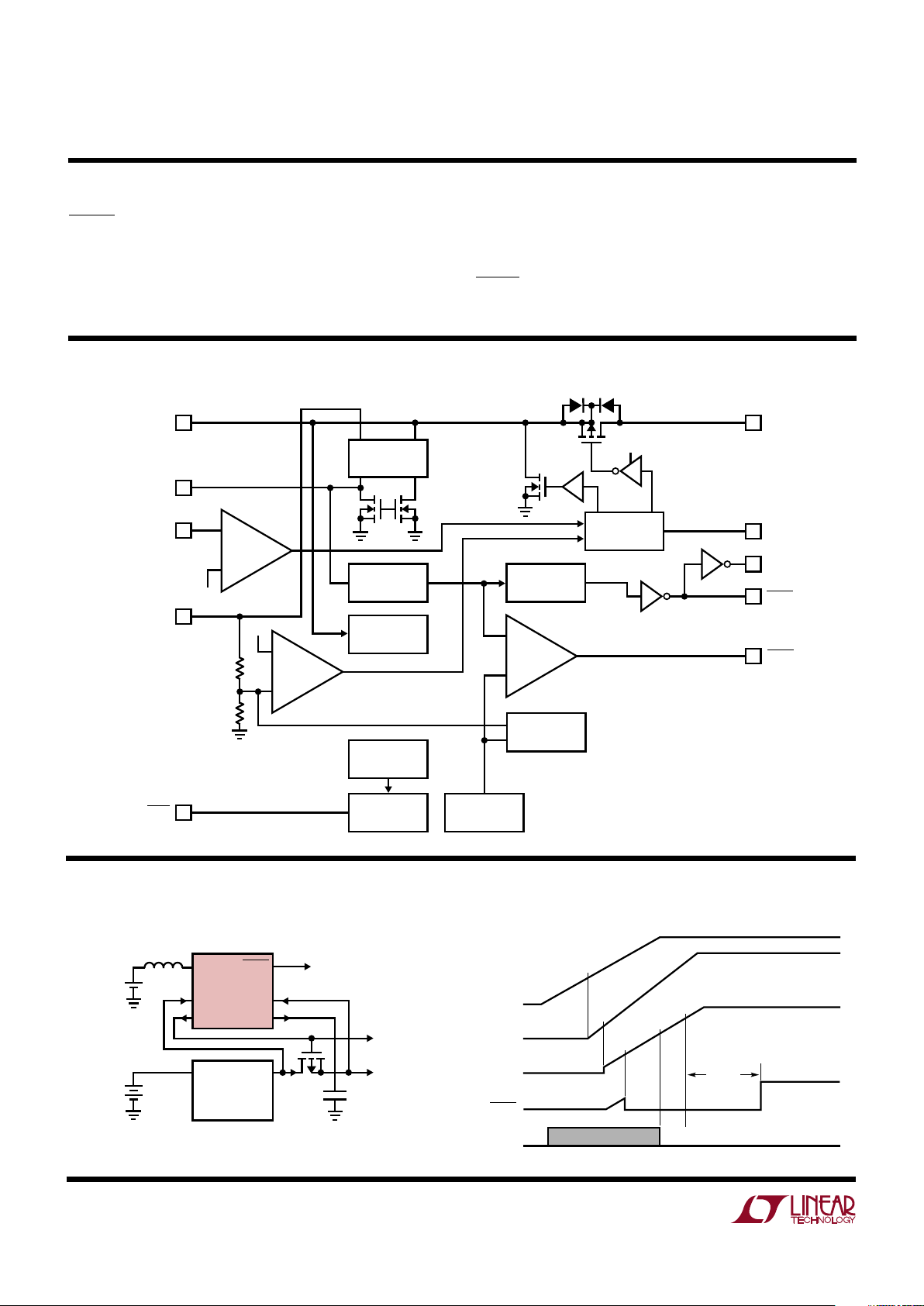
THERMAL
LIMIT
SHUTDOWN
LOGIC
BANDGAP
V
REF
= 1.272V
CHARGER
RESET
GENERATOR
BOOST/BACKUP
LOGIC
GAS GAUGE
V
REF
V
REF
V
CC
SHDN
PS
RESET
N1
P1
V
BAK
VCC/V
BAK
CTL
SW
–
+
–
+
UVLO
DETECTOR
RESET
BACKUP
LOBAT
1559 BD
BLOCK DIAGRAM
W
RESET (Pin 12): System Reset, Active High. This is a TTLcompatible output driver. It can connect to systems that
require active high logic. The RESET output will go high if
RESET is pulled low.
 Loading...