

Linear Technology LTC1553 Datasheet
FEATURES
■
5-Bit Digitally Programmable 1.8V to 3.5V Fixed
Output Voltage
■
Provides All Features Required by the
Intel
Pentium® II Processor VRM 8.2 DC/DC
Converter Specification
■
Flags for Power Good, Over-Temperature and
Overvoltage Fault
■
19A Output Current Capability from a 5V or 12V Supply
■
Dual N-Channel MOSFET Synchronous Driver
■
Initial Output Accuracy: ±1.5%
■
Excellent Output Accuracy: ±2% Typ Over Line,
Load and Temperature Variations
■
High Efficiency: Over 95% Possible
■
Adjustable Current Limit Without External Sense
Resistors
■
Fast Transient Response
■
Available in 20-Lead SSOP and SW Packages
U
APPLICATIONS
■
Power Supply for Pentium II, SPARC, ALPHA and
PA-RISC Microprocessors
■
High Power 5V or 12V to 1.8V-3.5V Regulators
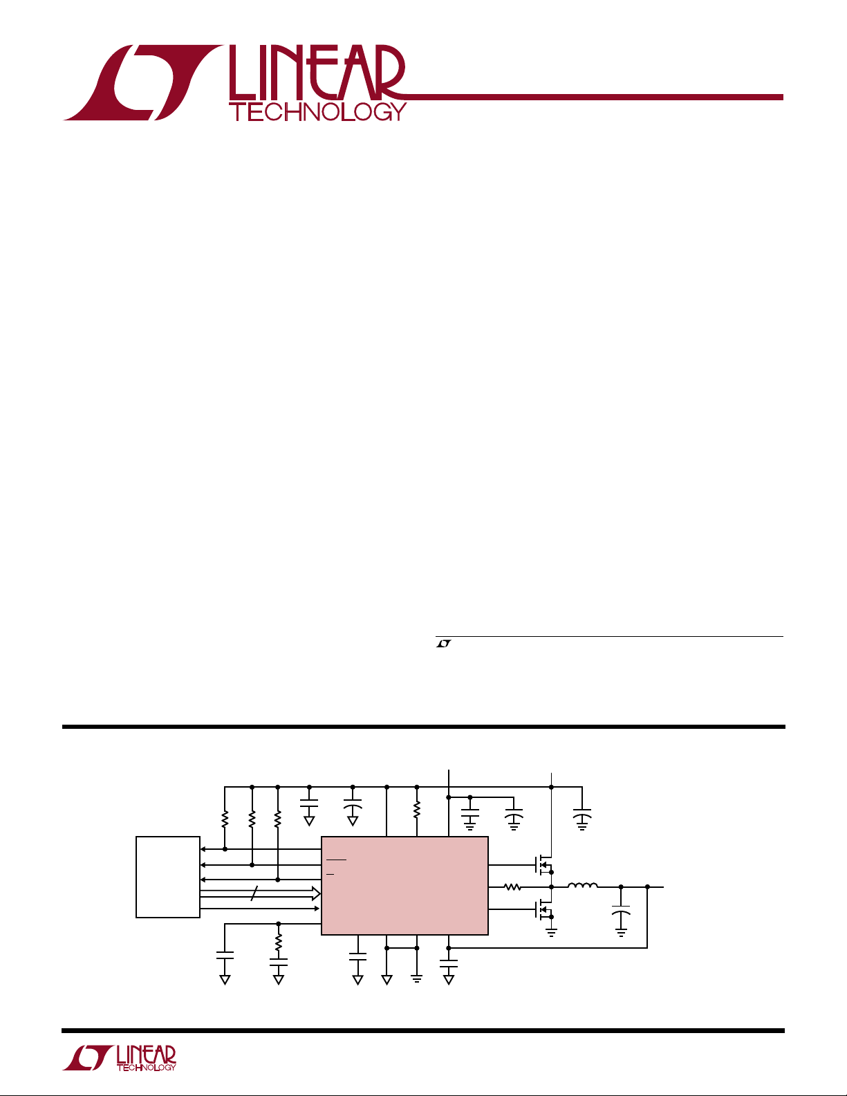
LTC1553
5-Bit Programmable
Synchronous Switching
Regulator Controller for
Pentium
®
II Processor
U
DESCRIPTION
The LTC®1553 is a high power, high efficiency switching
regulator controller optimized for 5V or 12V input to 1.8V-
3.5V output applications. It features a digitally programmable
output voltage, a precision internal reference and an internal
feedback system that provides output accuracy of ±1.5% at
room temperature and typically ±2% over-temperature, load
current and line voltage shifts. The LTC1553 uses a synchronous switching architecture with two external N-channel
output devices, providing high efficiency and eliminating the
need for a high power, high cost P-channel device. Additionally, it senses the output current across the on-resistance of
the upper N-channel FET, providing an adjustable current
limit without an external low value sense resistor.
The LTC1553 free-runs at 300kHz and can be synchronized
to a faster external clock if desired. It includes all the inputs
and outputs required to implement a power supply conforming to the
Converter Specification
, LTC and LT are registered trademarks of Linear Technology Corporation.
Pentium is a registered trademark of Intel Corporation.
Intel Pentium® II Processor VRM 8.2 DC/DC
.
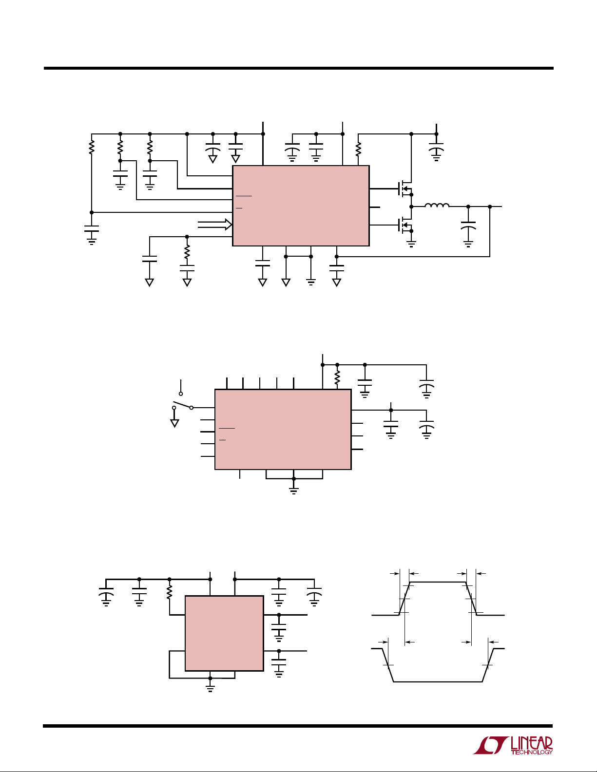
TYPICAL APPLICATION
5.6k
5.6k
PENTIUM® II
SYSTEM
C1
150pF
5
5.6k
R
8.2k
U
C
CC
0.01µF
+
0.1µF
10µF CIN**
PWRGD
FAULT
OT
VID0 TO VID4
OUTEN
COMP
C
SS
0.1µF
V
SS SGND GND SENSE
CC
LTC1553
PV
CC
12V
2.7k
I
MAX
0.1µF
PV
CC
G1
I
FB
G2
0.1µF
Figure 1. 5V to 1.8V-3.5V Supply Application
V
IN
5V
+
10µF
Q1*
20Ω
Q2*
*SILICONIX SUD50N03-10
**SANYO 10MV1200GX
†
COILTRONICS CTX02-13198 OR
PANASONIC 12TS-2R5SP
††
AVX TPSE337M006R0100
+
L
2µH
18A
O†
1200µF
× 4
C
OUT
330µF
× 7
V
OUT
1.8V TO
††
+
3.5V
14A
1553 F01
1
LTC1553
WW
W
U
ABSOLUTE MAXIMUM RATINGS
(Note 1)
Supply Voltage
VCC........................................................................ 9V
PVCC................................................................... 20V
Input Voltage
IFB (Note 2)............................................ PVCC + 0.3V
I
...................................................... –0.3V to 13V
MAX
All Other Inputs ......................... –0.3V to VCC + 0.3V
Digital Output Voltage............................... – 0.3V to 13V
IFB Input Current (Notes 2, 3) .......................... – 100mA
Operating Temperature Range ..................... 0°C to 70°C
Storage Temperature Range ................. –65°C to 150°C
Lead Temperature (Soldering, 10 sec.)................. 300°C
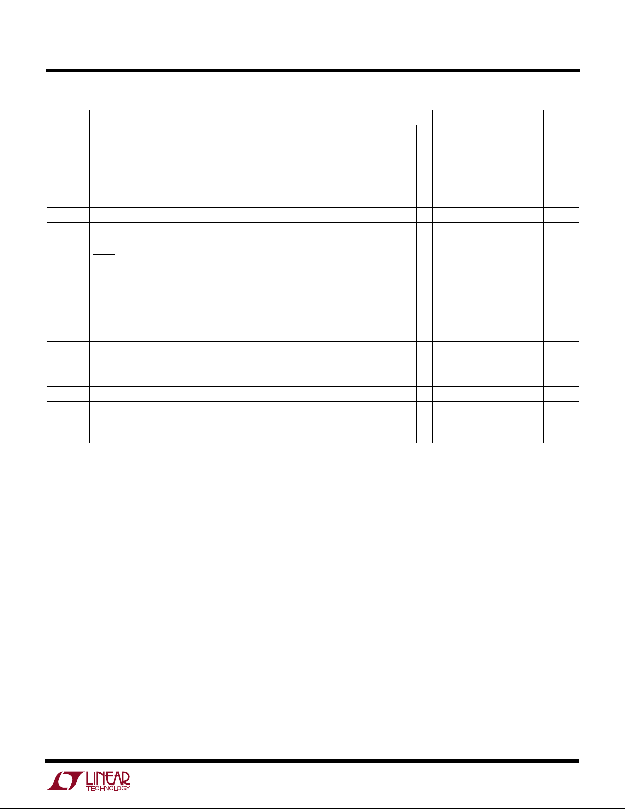
ELECTRICAL CHARACTERISTICS
VCC = 5V, PVCC = 12V, TA = 25°C, unless otherwise noted. (Note 3)
U
W
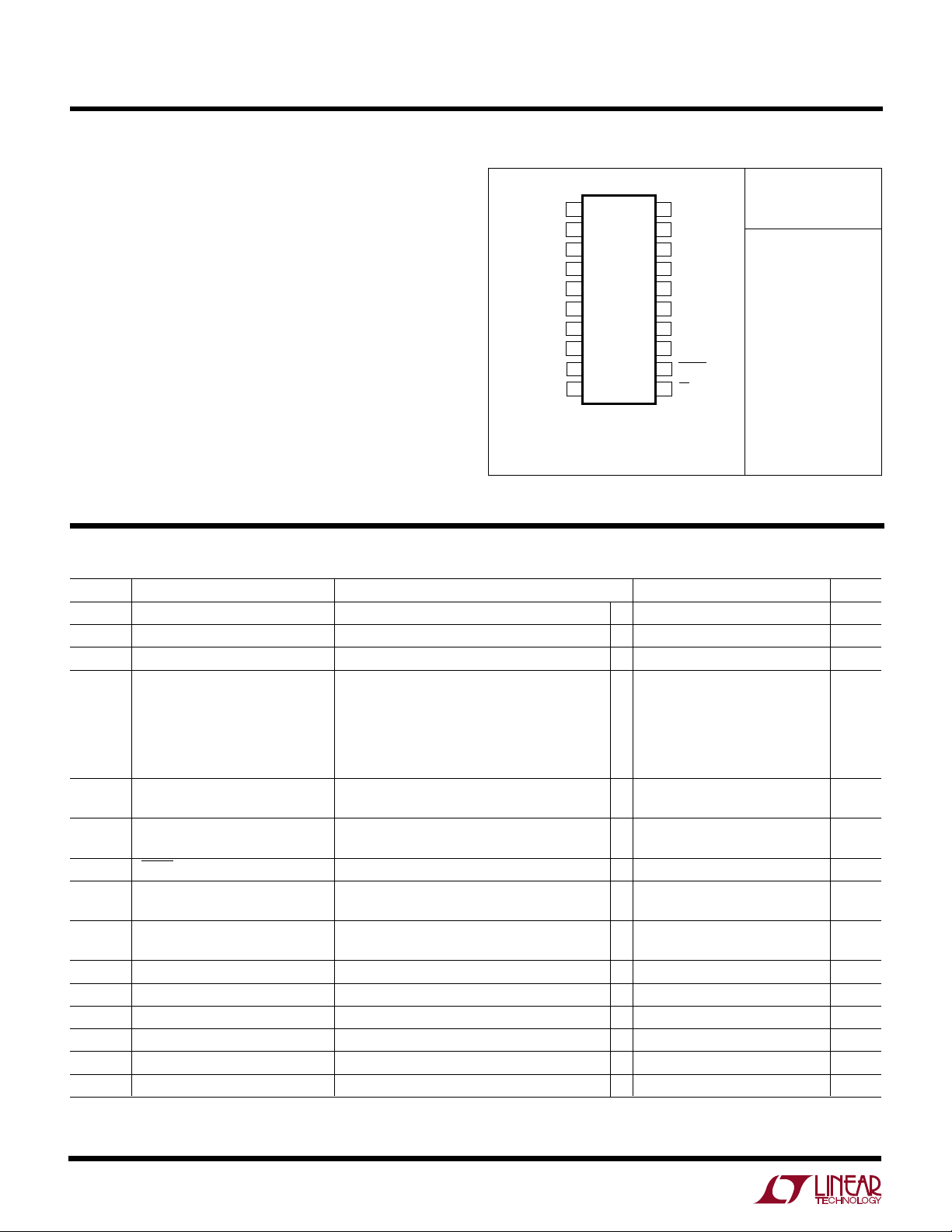
PACKAGE/ORDER INFORMATION
TOP VIEW
1
G2
2
PV
CC
3
GND
4
SGND
5
V
CC
6
SENSE
7
I
MAX
8
I
FB
9
SS
10
COMP
G PACKAGE
20-LEAD PLASTIC SSOP
T
= 125°C, θJA = 100°C/ W (G)
JMAX
= 125°C, θJA = 100°C/ W (SW)
T
JMAX
20-LEAD PLASTIC SO
G1
20
OUTEN
19
VID0
18
VID1
17
VID2
16
VID3
15
VID4
14
PWRGD
13
FAULT
12
OT
11
SW PACKAGE
Consult factory for Industrial and Military grade parts.
ORDER PART
NUMBER
LTC1553CG
LTC1553CSW
U
SYMBOL PARAMETER CONDITIONS MIN TYP MAX UNITS
V
PV
V
V
CC
CC
FB
OUT
Supply Voltage ● 4.5 8 V
Supply Voltage for G1, G2 ● 18 V
Internal Feedback Voltage (Note 4) 1.265 V
1.8V Initial Output Voltage With Respect to Rated Output Voltage (Figure 2) – 27 (–1.5%) 27 (+1.5%) mV
2.8V Initial Output Voltage – 42 (–1.5%) 42 (+ 1.5%) mV
3.5V Initial Output Voltage – 52 (–1.5%) 52 (+1.5%) mV
1.8V Initial Output Voltage
2.8V Initial Output Voltage
3.5V Initial Output Voltage
∆V
OUT
Output Load Regulation I
Output Line Regulation V
V
PWRGD
Positive Power Good Trip Point % Above Output Voltage (Figure 2) ● 57 %
Negative Power Good Trip Point % Below Output Voltage (Figure 2)
V
FAULT
I
CC
FAULT Trip Point % Above Output Voltage (Figure 2) ● 12 15 20 %
Operating Supply Current OUTEN = VCC = 5V (Note 5) (Figure 3) ● 800 1200 µA
Shutdown Supply Current OUTEN = 0, VID0 to VID4 Floating (Figure 3)
I
PVCC
f
OSC
V
V
G
g
BW
SAWL
SAWH
ERR
mERR
ERR
Supply Current PVCC = 12V, OUTEN = VCC (Note 6) (Figure 3) 15 mA
Internal Oscillator Frequency (Figure 4) ● 250 300 350 kHz
V
at Minimum Duty Cycle (Note 4) 1.8 V
COMP
V
at Maximum Duty Cycle (Note 4) 2.8 V
COMP
Error Amplifier Open-Loop DC Gain (Note 7) ● 40 53 dB
Error Amplifier Transconductance (Note 7) ● 0.9 1.6 2.3 millimho
Error Amplifier –3dB Bandwidth COMP = Open (Note 4) 400 kHz
= 0 to 14A (Note 4) (Figure 2) –5 mV
OUT
= 4.75V to 5.25V, I
IN
= 12V, OUTEN = 0, VID0 to VID4 Floating 1 µA
PV
CC
= 0 (Note 4)(Figure 2) ±1mV
OUT
● – 36 (–2%) 36 (+2%) mV
● – 56 (–2%) 56 (+2%) mV
● – 70 (–2%) 70 (+2%) mV
● –7 –5 %
● 130 250 µA
2
LTC1553
ELECTRICAL CHARACTERISTICS
VCC = 5V, PVCC = 12V, TA = 25°C, unless otherwise noted. (Note 3)
SYMBOL PARAMETER CONDITIONS MIN TYP MAX UNITS
I
IMAX
I
SS
I
SSIL
I
SSHIL
I
Sink Current V
MAX
Soft Start Source Current VSS = 0V, V
Maximum Soft Start Sink Current V
IMAX
SENSE
= V
= V
CC
IMAX
OUT
Under Current Limit (Notes 8, 9), V
Soft Start Sink Current Under Hard V
SENSE
= 0V, V
= 0V, V
, V
IMAX
= V
SS
IMAX
IFB
= VCC, V
CC
= VCC, V
● 150 180 220 µA
= V
CC
= 0V ● 30 60 150 µA
IFB
= 0V ● 20 45 mA
IFB
● –13 –10 –7 µA
Current Limit
t
SSHIL
t
PWRGD
t
PWRBAD
t
FAULT
t
OT
V
OT
V
OTDD
V
SHDN
tr, t
f
t
NOL
DC
MAX
V
IH
V
IL
R
IN
Hard Current Limit Hold Time V
Power Good Response Time↑ V
Power Good Response Time↓ V
FAULT Response Time V
= 0V, V
SENSE
SENSE
SENSE
SENSE
IMAX
↑ from 0V to Rated V
↓ from Rated V
↑ from Rated V
= 4V, V
↓ from 5V (Note 4) 500 µs
IFB
OUT
to 0V ● 200 500 1000 µs
OUT
to V
OUT
CC
● 0.5 1 2 ms
● 200 500 1000 µs
OT Response Time OUTEN↓, VID0 to VID4 = 0 (Note 10) (Figure 3) ● 15 40 60 µs
Over-Temperature Trip Point OUTEN↓, VID0 to VID4 = 0 (Note 10) (Figure 3) ● 1.9 2 2.12 V
Over-Temperature Driver Disable OUTEN↓, VID0 to VID4 = 0 (Note 10) (Figure 3) ● 1.6 1.7 1.8 V
Shutdown OUTEN↓, VID0 to VID4 = 0 (Note 10) (Figure 3) ● 0.8 V
Driver Rise and Fall Time (Figure 4) ● 90 150 ns
Driver Nonoverlap Time (Figure 4) ● 30 100 ns
Maximum G1 Duty Cycle (Figure 4) ● 77 84 88 %
VID0 to VID4 Input High Voltage ● 2V
VID0 to VID4 Input Low Voltage ● 0.8 V
VID0 to VID4 Internal Pull-Up ● 10 20 kΩ
Resistance
I
SINK
Digital Output Sink Current ● 10 mA
The ● denotes specifications which apply over the full operating
temperature range.
Note 1: Absolute Maximum Ratings are those values beyond which the life
of a device may be impaired.
Note 2: When I
is taken below GND, it will be clamped by an internal
FB
diode. This pin can handle input currents greater than 100mA below GND
without latchup. In the positive direction, it is not clamped to V
or PVCC.
CC
Note 3: All currents into device pins are positive; all currents out of the
device pins are negative. All voltages are referenced to ground unless
otherwise specified.
Note 4: This parameter is guaranteed by correlation and is not tested
directly.
Note 5: The LTC1553 goes into the shutdown mode if VID0 to VID4 are
floating. Due to the internal pull-up resistors, there will be an additional
0.25mA/pin if any of the VID0 to VID4 pins are pulled low.
Note 6: Supply current in normal operation is dominated by the current
needed to charge and discharge the external FET gates. This will vary with
the LTC1553 operating frequency, supply voltage and the external FETs
used.
Note 7: The open-loop DC gain and transconductance from the SENSE pin to
COMP pin will be (G
)(1.265/3.3) and (g
ERR
)(1.265/3.3) respectively.
mERR
Note 8: The current limiting amplifier can sink but cannot source current.
Under normal (not current limited) operation, the output current will be zero.
Note 9: Under typical soft current limit, the net soft start discharge current
will be 60µA (I
) + [–10µA(ISS)] = 50µ A. The soft start sink-to-source
SSIL
current ratio is designed to be 6:1.
Note 10: When VID0 to VID4 are all HIGH, the LTC1553 will be forced to
shut down internally. The OUTEN trip voltages are guaranteed by design for
all other input codes.
3
LTC1553
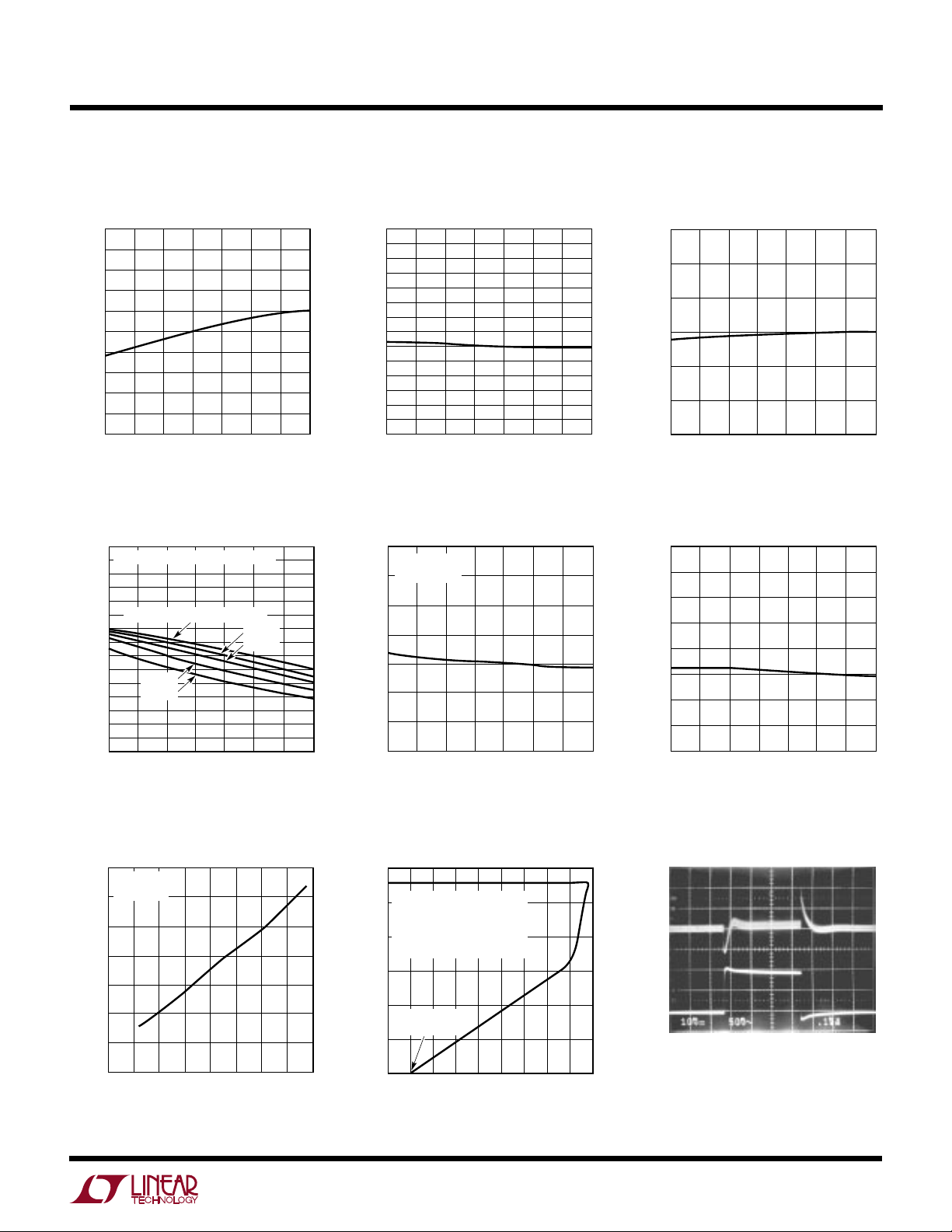
OUTPUT CURRENT (A)
0
OUTPUT VOLTAGE (V)
2.825
4
1533 G03
2.820
2.815
2.810
2.805
2.800
2.795
2.790
2.785
2.780
2.775
123
5
67891011121314
REFER TO TYPICAL APPLICATION
CIRCUIT FIGURE 1
V
IN
= 5V, PVCC = 12V, TA = 25°C
TEMPERATURE (°C)
–50
OVER-TEMPERATURE TRIP POINT (V)
1.96
2.08
2.10
2.12
0
50
75
1553 G06
1.92
2.04
2.00
1.94
2.06
1.90
2.02
1.98
–25
25
100
125
UW
TYPICAL PERFORMANCE CHARACTERISTICS
Typical 2.8V V
140
TOTAL SAMPLE SIZE = 1500
120
100
80
60
NUMBER OF UNITS
40
20
0
2.775
2.785
25°C 100°C
OUTPUT VOLTAGE (V)
OUT
2.795
Distribution
2.805 2.815
1553 G01
2.825
Efficiency vs Load Current
100
90
A
B
80
70
REFER TO TYPICAL APPLICATION
60
CIRCUIT FIGURE 1
= 5V, PVCC = 12V, V
V
50
IN
= 330µF ×7, LO = 2µH
C
OUT
40
EFFICIENCY (%)
A: Q1 = 1 × SUD50N03-10
Q2 = 1 × SUD50N03-10
30
B: Q1 = 2 × SUD50N03-10
20
Q2 = 1 × SUD50N03-10
NO FAN
10
Q1 IS MOUNTED ON 1IN
0
0
2
0.3
4
LOAD CURRENT (A)
Line Regulation Output Temperature Drift
2.825
REFER TO TYPICAL APPLICATION
2.820
CIRCUIT FIGURE 1
OUTPUT = NO LOAD
2.815
2.810
2.805
2.800
2.795
2.790
OUTPUT VOLTAGE (V)
2.785
2.780
2.775
4.75
T
A
= 25°C
4.85
5.05
4.95
INPUT VOLTAGE (V)
5.15
5.25
1553 G04
2.860
2.850
2.840
2.830
2.820
2.810
2.800
2.790
2.780
OUTPUT VOLTAGE (V)
2.770
2.660
2.750
2.740
–50
–25
0
TEMPERATURE (°C)
= 2.8V,
OUT
2
COPPER AREA
6 8 10 12 14
1533 G02
50
25
75
100
1553 G05
Load Regulation
Over-Temperature Trip Point
vs Temperature
125
Over-Temperature Driver Disable
vs Temperature
1.80
1.78
1.76
1.74
1.72
1.70
1.68
1.66
1.64
1.62
OVER-TEMPERATURE DRIVER DISABLE (V)
1.60
–50
4
0
–25
TEMPERATURE (°C)
Error Amplifier Transconductance
vs Temperature
2.3
2.1
1.9
1.7
1.5
1.3
1.1
50
25
75
100
125
1553 G07
0.9
ERROR AMPLIFIER TRANSCONDUCTANCE (millimho)
–50
–25 0
TEMPERATURE (°C)
50 100 125
25 75
1553 G08
Error Amplifier Open-Loop
DC Gain vs Temperature
60
55
50
45
ERROR AMPLIFIER OPEN-LOOP DC GAIN (dB)
40
–50
–25 0 25 50
TEMPERATURE (°C)
75 100 125
1553 G09
UW
TYPICAL PERFORMANCE CHARACTERISTICS
LTC1553
Oscillator Frequency
vs Temperature
350
340
330
320
310
300
290
280
270
OSCILLATOR FREQUENCY (kHz)
260
250
–50
–25
25
0
TEMPERATURE (°C)
Maximum G1 Duty Cycle
vs Temperature
92
OSCILLATOR FREQUENCY = 300kHz
90
88
G1, G2 CAPACITANCE = 1100pF
86
84
–50
5500pF
7700pF
–25 0
25 75
TEMPERATURE (°C)
82
80
MAXIMUM G1 DUTY CYCLE (%)
78
50
75
2200pF
3300pF
50 100 125
100
125
1553 G10
1553 G13
I
Sink Current
MAX
vs Temperature
220
210
200
190
180
SINK CURRENT (µA)
170
MAX
I
160
150
–50
0
–25
TEMPERATURE (°C)
25
VCC Operating Supply Current
vs Temperature
1.2
VCC = 5V
= 300kHz
f
OSC
1.1
1.0
0.9
0.8
0.7
OPERATING SUPPLY CURRENT (mA)
0.6
CC
V
0.5
–50
–25 0
25 75
TEMPERATURE (°C)
75
50 125
50 100 125
100
1553 G11
1553 G14
Soft Start Source Current
vs Temperature
–7
–8
–9
–10
–11
–12
SOFT START SOURCE CURRENT (µA)
–13
–50
–25 0
TEMPERATURE (°C)
50 100 125
25 75
VCC Shutdown Supply Current
vs Temperature
250
225
200
175
150
125
100
SHUTDOWN SUPPLY CURRENT (mA)
75
CC
V
50
–25 0 50
–50
25
TEMPERATURE (°C)
1553 G12
75 100 125
1553 G15
PVCC Supply Current
vs Gate Capacitance
70
PVCC = 12V
= 25°C
T
A
60
50
40
30
SUPPLY CURRENT (mA)
20
CC
PV
10
0
2000 4000 8000
0
GATE CAPACITANCE (pF)
6000
1553 G16
Output Over Current Protection
3.0
Q1 CASE = 90°C, V
2.5
Q1 = 2 × MTD20N03HDL
Q2 = 1 × MTD20N03HDL
2.0
1.5
1.0
OUTPUT VOLTAGE (V)
0.5
= 2.7k, R
R
IMAX
SS CAP = 0.01µF
SHORT-CIRCUIT
CURRENT
0
26
0
4
OUTPUT CURRENT (A)
= 2.8V
OUT
= 20Ω,
IFB
10 18
8
Transient Response
50mV/DIV
5A/DIV
100µs/DIV
14
16
12
1553 G17
1553 G18
5

LTC1553
PIN FUNCTIONS
UUU
G2 (Pin 1): Gate Drive for the Lower N-Channel MOSFET,
Q2. This output will swing from PVCC to GND. It will always
be low when G1 is high or when the output is disabled. To
prevent undershoot during a soft start cycle, G2 is held low
until G1 first goes high.
PVCC (Pin 2): Power Supply for G1 and G2. PVCC must be
connected to a potential of at least VIN + V
VIN = 5V, PVCC can be generated using a simple charge
pump connected to the switching node between Q1 and
Q2 (see Figure 7), or it can be connected to an auxiliary 12V
supply if one exists. For applications where VIN = 12V,
PVCC can be generated using a 17V charge pump (see
Figure 9).
GND (Pin 3): Power Ground. GND should be connected to
a low impedance ground plane in close proximity to the
source of Q2.
SGND (Pin 4): Signal Ground. SGND is connected to the
low power internal circuitry and should be connected to
the negative terminal of the output capacitor where it
returns to the ground plane. GND and SGND should be
shorted right at the LTC1553.
VCC (Pin 5): Power Supply. Power for the internal low
power circuity. VCC should be wired separately from the
drain of Q1 if they share the same supply. A 10µ F bypass
capacitor is recommended from this pin to SGND.
SENSE (Pin 6): Output Voltage Pin. Connect to the positive
terminal of the output capacitor. There is an internal 120k
resistor connected from this pin to SGND. SENSE is a very
sensitive pin; for optimum performance, connect an external 0.1µ F capacitor from this pin to SGND. By connecting
a small external resistor between the output capacitor and
the SENSE pin, the initial output voltage can be raised
slightly. Since the internal divider has a nominal impedance of 120kΩ, a 1200Ω series resistor will raise the
nominal output voltage by 1%. If an external resistor is
used, the value of the 0.1µF capacitor on the SENSE pin
must be greatly reduced or loop phase margin will suffer.
Set a time constant for the RC combination of approximately 0.1µ s. So, for example, with a 1200Ω resistor, set
C = 83pF. Use a standard 100pF capacitor.
GS(ON)Q1
. If
I
(Pin 7): Current Limit Threshold. Current limit is set
MAX
by the voltage drop across an external resistor connected
between the drain of Q1 and I
pull-down at I
IFB (Pin 8): Current Limit Sense Pin. Connect to the
switching node between the source of Q1 and the drain of
Q2. If IFB drops below I
will go into current limit. The current limit circuit can be
disabled by floating I
an external 10k resistor. For VIN = 12V, a 15V Zener diode
from IFB to GND is recommended to prevent the voltage
spike at IFB from exceeding the maximum voltage rating.
SS (Pin 9): Soft Start. Connect to an external capacitor to
implement a soft start function. During moderate overload
conditions, the soft start capacitor will be discharged
slowly in order to reduce the duty cycle. In hard current
limit, the soft start capacitor will be forced low immediately and the LTC1553 will rerun a complete soft start
cycle. CSS must be selected such that during power-up the
current through Q1 will not exceed the current limit value.
COMP (Pin 10): External Compensation. The COMP pin is
connected directly to the output of the error amplifier and
the input of the PWM comparator. An RC+ C network is
used at this node to compensate the feedback loop to
provide optimum transient response.
OT (Pin 11): Over-Temperature Fault. OT is an open-drain
output and will be pulled low if OUTEN is less than 2V. If
OUTEN = 0, OT pulls low.
FAULT (Pin 12): Overvoltage Fault. FAULT is an opendrain output. If V
output voltage, FAULT will go low and G1 and G2 will be
disabled. Once triggered, the LTC1553 will remain in this
state until the power supply is recycled or the OUTEN pin
is toggled. If OUTEN = 0, FAULT floats or is pulled high by
an external resistor.
PWRGD (Pin 13): Power Good. This is an open-drain
signal to indicate validity of output voltage. A high indicates that the output has settled to within ±5% of the rated
output for more than 1ms. PWRGD will go low if the output
is out of regulation for more than 500µs. If OUTEN = 0,
PWRGD pulls low.
MAX
.
MAX
and shorting IFB to VCC through
MAX
reaches 15% above the nominal
OUT
. There is a 180µ A internal
MAX
when G1 is on, the LTC1553
6
UUU
PIN FUNCTIONS
LTC1553
VID0, VID1, VID2, VID3, VID4 (Pins 18, 17, 16, 15, 14):
Digital Voltage Select. TTL inputs used to set the regulated
output voltage required by the processor (Table 3). There
is an internal 20kΩ pull-up at each pin. When all five VID
n
pins are high or floating, the chip will shut down.
OUTEN (Pin 19): Output Enable. TTL input which enables
the output voltage. The external MOSFET temperature can
be monitored with an external thermistor as shown in
Figure 13. When the OUTEN input voltage drops below 2V,
W
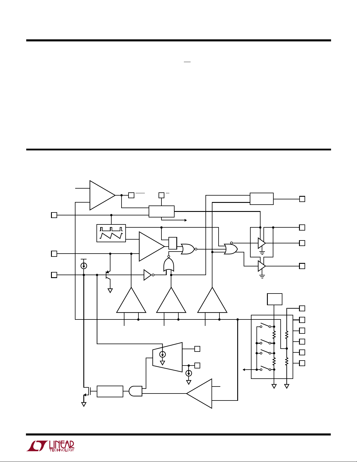
BLOCK DIAGRAM
OUTEN
COMP
19
10
115% V
REF
+
FC
FAULT
12
OT
11
–
LOGIC
–
PWM
+
R
S
OT trips. As OUTEN drops below 1.7V, the drivers are
internally disabled to prevent the MOSFETs from heating
further. If OUTEN is less than 1.2V for longer than 30µs,
the LTC1553 will enter shutdown mode. The internal
oscillator can be synchronized to a faster external clock by
applying the external clocking signal to the OUTEN pin.
G1 (Pin 20): Gate Drive for the Upper N-Channel MOSFET,
Q1. This output will swing from PVCC to GND. It will always
be low when G2 is high or the output is disabled.
DISDR
SYSTEM
POWER
DOWN
DELAY
13
2
20
PWRGD
PV
CC
G1
I
SS
SS
9
Q
SS
ERR
+
–
V
REF
HCL MONOMHCL
MIN
+
–
V
– 5% V
REF
–
CC
+
I
MAX
8
7
REF
LVC
I
I
FB
MAX
+ 5%
MAX
–+
+
0.5V
0.7V
REF
REF
FB
V
REF
/
BG
DAC
–
1
6
18
17
16
15
14
G2
SENSE
VID0
VID1
VID2
VID3
VID4
1553 BD
7
LTC1553
TEST CIRCUITS
3k3k
0.1µF
PV
12V
CC
10k
V
IN
5V
CIN**
+
1200µF
× 4
V
CC
5V
3k
10µF
0.1µF
++
10µF
100pF
100pF
100pF
VID0 TO VID4
C1
150pF
V
CC
R
C
8.2k
CC
0.01µF
VID0 VID1 VID2 VID3 VID4
VID0 VID1 VID2 VID3 VID4
OUTEN
PWRGD
NC
FAULT
NC
OT
NC
COMP
NC
V
CC
OUTEN
PWRGD
FAULT
OT
VID0 TO VID4
COMP
SS SGND GND SENSE
0.1µF
LTC1553
Figure 2
V
CC
V
CC
LTC1553
SS SGND GND SENSE
PV
I
PV
I
MAX
I
FB
CC
G1
NC
I
MAX
G2
0.1µF
10k
FB
CC
G1
NC
NC
G2
NC
*SILICONIX SUD50N03-10
**SANYO 10MV1200GX
PANASONIC 12TS-2R5SP
††
0.1µF
PV
CC
0.1µF
L
O†
Q1*
2µH
15A
††
C
+
Q2*
†
COILTRONICS CTX02-13198 OR
AVX TPSE337M006R0100
OUT
330µF
× 7
+
10µF
+
10µF
V
OUT
1553 F02
8
NC
1553 F03
Figure 3
V
PV
CC
CC
5V
12V
+
10µF
0.1µF
10k
I
FB
SENSE
SGND GND
V
CC
LTC1553
PV
CC
G1
G2
0.1µF
5000pF
5000pF
+
10µF
G1 RISE/FALL
G2 RISE/FALL
t
r
90%
50%
10%
t
NOL
50% 50%
90%
50%
10%
t
f
t
NOL
1553 F04
Figure 4
 Loading...