

Linear Technology LTC1551L, LTC1550L Datasheet
FEATURES
LTC1550L/LTC1551L
Low Noise, Switched
Capacitor Regulated
Voltage Inverters
U
DESCRIPTIO
■
Regulated Negative Voltage from a Single
Positive Supply
■
Low Output Ripple: Less Than 1mV
■
High Charge Pump Frequency: 900kHz
■
Small Charge Pump Capacitors: 0.1µF
■
Requires Only Four External Capacitors
■
Fixed –4.1V, –2.5V, –2V or Adjustable Output
■
Shutdown Mode Drops Supply Current to <1µA
■
High Output Current: Up to 20mA (Depending on
VCC to V
■
Output Regulation: 2.5% Over Line, Load and
OUT
Range)
P-P
Typ
Temperature
■
Available in 8-Lead MSOP, 8-Lead Narrow SO and
16-Lead Narrow SSOP
U
APPLICATIO S
■
GaAs FET Bias Generators
■
Negative Supply Generators
■
Battery-Powered Systems
■
Single Supply Applications
The LTC®1550L/LTC1551L are switched capacitor charge
pump voltage inverters which include internal linear postregulators to minimize output ripple. The LTC1550L fixed
output voltage versions include –4.1V, –2.5V and –2V with
ripple voltages typically below 1mV
. The LTC1550L is
P-P
also available in an adjustable output voltage version. The
LTC1550L/LTC1551L are ideal for use as bias voltage
generators for GaAs transmitter FETs in portable RF and
cellular telephone applications.
The LTC1550L/LTC1551L operate from single 2.7V to
5.5V supplies and draw typical quiescent currents of
3.5mA with a 5V supply. Each device includes a TTL
compatible Shutdown pin which drops supply current to
0.2µA typically. The LTC1550L Shutdown pin is active low
(SHDN), while the LTC1551L Shutdown pin is active high
(SHDN). Only four external components are required: an
input bypass capacitor, two 0.1µF charge pump capacitors
and a filter capacitor at the linear regulator output. The
adjustable LTC1550L/LTC1551L require two additional resistors to set the output voltage. The LTC1550L/LTC1551L
will supply up to 20mA (depending on VCC to V
OUT
range),
while maintaining guaranteed output regulation of ±2.5%.
, LTC and LT are registered trademarks of Linear Technology Corporation.
U
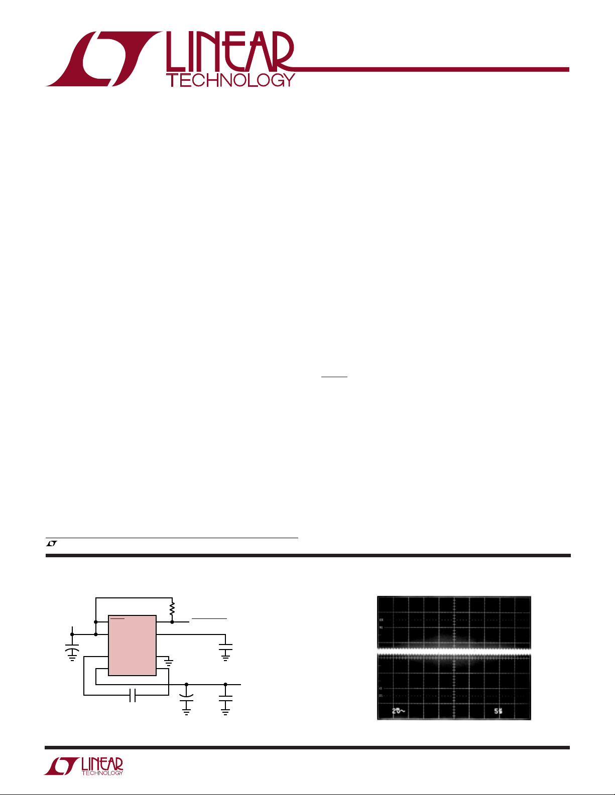
TYPICAL APPLICATIO
R1
10k
8
7
6
5
–
POWER VALID
C
OUT
+
10µF
P-P
2.2µF
C
IN
1
2
3
4
SHDN
V
CC
LTC1550L-2
+
C1
V
OUT
C1
0.1µF
REG
CP
OUT
GND
C1
3.6V
+
Figure 1. –2V Generator with 1mV
C
CP
0.1µF
V
OUT
I
LOAD
C
L
0.1µF
Noise
= –2V
= 5mA
1550L/51L TA01
Both fixed voltage and adjustable LTC1550L/LTC1551L
are available in 8-lead MSOP and SO plastic packages: the
adjustable LTC1550L is also available in a 16-pin SSOP
with the REG pin.
V
Output Noise and Ripple
OUT
V
OUT
AC COUPLED
2mV/DIV
5µs/DIV 1550L/51L TA01a
1
LTC1550L/LTC1551L
WW
W
ABSOLUTE MAXIMUM RATINGS
U
(Note 1)
Supply Voltage ...................................................... 5.5V
Output Voltage............................. 0.3V to (VCC – 10.5V)
Total Voltage, VCC to CP
..........................................
OUT
10.8V
Input Voltage (SHDN Pin) ........... –0.3V to (VCC + 0.3V)
Input Voltage (REG Pin) ............................. –0.3V to 6V
Output Short-Circuit Duration.............................. 30 sec
U
W
U
PACKAGE/ORDER INFORMATION
TOP VIEW
1
SHDN*
2
V
CC
+
3
C1
4
V
OUT
MS8 PACKAGE
8-LEAD PLASTIC MSOP
*SHDN FOR LTC1550L, SHDN FOR LTC1551L
*FOR ADJUSTABLE VERSION
T
= 150°C, θJA = 200°C/W
JMAX
ORDER PART NUMBER
LTC1550LCMS8
LTC1550LCMS8-2
LTC1550LCMS8-2.5
LTC1550LCMS8-4.1
MS8 PART MARKING
LTEG
LTGR
LTFV
LTEH
8
REG (ADJ*)
7
CP
OUT
6
GND
–
5
C1
LTC1551LCMS8
LTC1551LCMS8-4.1
LTFQ
LTFT
SHDN*
V
CC
C1
V
OUT
*SHDN FOR LTC1550L, SHDN FOR LTC1551L
ORDER PART NUMBER
Commercial Temperature Range ................. 0°C to 70°C
Extended Commercial Operating
Temperature Range (Note 3) .............. –40°C to 85°C
Industrial Temperature Range ................ – 40°C to 85°C
Storage Temperature Range ................ –65°C to 150°C
Lead Temperature (Soldering, 10 sec)................. 300°C
TOP VIEW
1
2
+
3
4
S8 PACKAGE
8-LEAD PLASTIC SO
*FOR ADJUSTABLE VERSION
T
= 150°C, θJA = 135°C/W
JMAX
LTC1550LCS8
8
REG (ADJ*)
7
CP
6
GND
C1
5
OUT
–
NC
C1
NC
V
OUT
C1
PGND
AGND
NC
T
ORDER PART NUMBER
TOP VIEW
1
+
2
3
4
–
5
6
7
8
GN PACKAGE
16-LEAD PLASTIC SSOP
= 150°C, θJA = 150°C/W
JMAX
LTC1550LCS8-2
LTC1550LCS8-2.5
LTC1550LCS8-4.1
LTC1550LCGN
LTC1550LIGN
LTC1551LCS8
LTC1551LCS8-4.1
GN PART MARKING
1550L
1550LI
16
V
CC
15
SHDN
14
REG
13
NC
12
ADJ
11
CP
OUT
10
NC
9
NC
Consult factory for Military grade parts and additional voltage options.
ELECTRICAL CHARACTERISTICS
The ● denotes the specifications which apply over the full operating temperature range, otherwise specifications are at TA = 25°C.
VCC = 2.7V to 5.25V, C1 = C
SYMBOL PARAMETER CONDITIONS MIN TYP MAX UNITS
V
CC
V
REF
∆V
∆(VCC – V
I
S
Supply Voltage
(Adjustable, Fixed –2V)
(Fixed –2.5V)
(Fixed –4.1V) ● 4.5 5.25 V
Reference Voltage VCC = 5V, ADJ = GND, V
Reference Voltage I
REF
Line Regulation
OUT)
Supply Current VCC = 5V, V
= 0.1µF, C
CP
= 10µF, TA = 25°C unless otherwise specified. (Note 3)
OUT
= –V
REF
OUT
= 0mA, 2.7V ≤ VCC ≤ 5.25V 2.5 mV/V
OUT
= VCC (LTC1550L) or GND (LTC1551L) ● 3.65 7 mA
VCC = 5V, V
SHDN
= GND (LTC1550L) or VCC (LTC1551L) ● 0.2 10 µA
SHDN
● 2.7 5.25 V
● 3.05 5.25 V
1.225 V
2
LTC1550L/LTC1551L
ELECTRICAL CHARACTERISTICS
The ● denotes the specifications which apply over the full operating temperature range, otherwise specifications are at TA = 25°C.
VCC = 2.7V to 5.25V, C1 = C
SYMBOL PARAMETER CONDITIONS MIN TYP MAX UNITS
f
OSC
V
OL
I
REG
V
IH
V
IL
I
IN
t
ON
V
OUT
V
OUT
V
OUT
V
OUT
V
OUT
V
OUT
V
OUT
I
SC
V
RIPPLE
Note 1: Absolute Maximum Ratings are those values beyond which the life
of a device may be impaired.
Note 2: All currents into device pins are positive; all currents out of device
pins are negative. All voltages are referenced to ground unless otherwise
specified. All typicals are given at T
Internal Oscillator Frequency 900 kHz
REG Output Low Voltage I
REG Sink Current V
SHDN Input High Voltage VCC = 5V ● 2V
SHDN Input Low Voltage VCC = 5V ● 0.8 V
SHDN Input Current V
Turn-On Time VCC = 5V, I
Output Regulation 2.7V ≤ VCC ≤ 5.25V, 0 ≤ I
(LTC1550L/LTC1551L) 2.8V ≤ V
Output Regulation 2.7V ≤ VCC ≤ 5.25V, 0 ≤ I
(LTC1550L/LTC1550L-2/ 3.1V ≤ V
LTC1551L) 3.75V ≤ VCC ≤ 5.25V, 0 ≤ I
Output Regulation 3.05V ≤ VCC ≤ 5.25V, 0 ≤ I
(LTC1550L/LTC1550L-2.5/ 3.45V ≤ V
LTC1551L) 4.1V ≤ VCC ≤ 5.25V, 0 ≤ I
Output Regulation 3.45V ≤ VCC ≤ 5.25V, 0 ≤ I
(LTC1550L/LTC1551L) 3.85V ≤ V
Output Regulation 3.9V ≤ VCC ≤ 5.25V, 0 ≤ I
(LTC1550L/LTC1551L) 4.2V ≤ V
Output Regulation 4.5V ≤ VCC ≤ 5.25V, 0 ≤ I
(LTC1550L/LTC1550L-4.1) 4.75V ≤ V
(LTC1551L/LTC1551L-4.1)
Output Regulation 4.8V ≤ VCC ≤ 5.25V, 0 ≤ I
(LTC1550L/LTC1551L)) 5.1V ≤ VCC ≤ 5.25V, 0 ≤ I
Output Short-Circuit Current V
Output Ripple Voltage 1mV
= 0.1µF, C
CP
= 25°C.
A
= 10µF, TA = 25°C unless otherwise specified. (Note 3)
OUT
= 1mA, VCC = 5V ● 0.1 0.8 V
REG
= 0.8V, VCC = 5V ● 410 mA
REG
= VCC (All LTC1550L Versions) ● 0.1 1 µA
SHDN
V
= VCC (All LTC1551L Versions) ● 520 µA
SHDN
= 10mA, –1.5V ≤ V
OUT
≤ 4.1V ● 15ms
OUT
(LTC1550L/LTC1551L)
V
= 5V, I
CC
= 5mA, V
OUT
= –4.5V ● 15ms
OUT
(LTC1550L/LTC1551L)
V
= 5V, I
CC
= 10mA, V
OUT
= –2V ● 15ms
OUT
(LTC1550L-2)
V
= 5V, I
CC
= 10mA, V
OUT
= –2.5V ● 15ms
OUT
(LTC1550L-2.5)
V
= 5V, I
CC
= 10mA, V
OUT
= –4.1V ● 15ms
OUT
(LTC1550L-4.1/LTC1551L-4.1)
≤ 5mA ● –1.537 –1.5 –1.463 V
≤ 5.25V, 0 ≤ I
CC
3.5V ≤ VCC ≤ 5.25V, 0 ≤ I
≤ 5.25V, 0 ≤ I
CC
≤ 5.25V, 0 ≤ I
CC
≤ 5.25V, 0 ≤ I
CC
4.5V ≤ VCC ≤ 5.25V, 0 ≤ I
≤ 5.25V, 0 ≤ I
CC
4.85V ≤ VCC ≤ 5.25V, 0 ≤ I
≤ 5.25V, 0 ≤ I
CC
= 0V, VCC = 5.25V ● 80 200 mA
OUT
OUT
≤ 10mA ● –1.537 –1.5 –1.463 V
OUT
≤ 20mA ● –1.537 –1.5 –1.463 V
OUT
≤ 5mA ● –2.05 – 2.0 –1.95 V
OUT
≤ 10mA ● –2.05 – 2.0 –1.95 V
OUT
≤ 20mA ● –2.05 – 2.0 –1.95 V
OUT
≤ 5mA ● –2.562 –2.5 –2.438 V
OUT
≤ 10mA ● –2.562 –2.5 –2.438 V
OUT
≤ 20mA ● –2.562 –2.5 –2.438 V
OUT
≤ 5mA ● –3.075 –3.0 –2.925 V
OUT
≤ 10mA ● –3.075 –3.0 –2.925 V
OUT
≤ 20mA ● –3.075 –3.0 –2.925 V
OUT
≤ 5mA ● –3.587 –3.5 –3.413 V
OUT
≤ 10mA ● –3.587 –3.5 –3.413 V
OUT
≤ 20mA ● –3.587 –3.5 –3.413 V
OUT
≤ 5mA ● –4.203 –4.1 –3.998 V
OUT
≤ 10mA ● –4.203 –4.1 –3.998 V
OUT
≤ 5mA ● –4.613 –4.5 –4.388 V
OUT
≤ 10mA ● –4.613 –4.5 –4.388 V
OUT
Note 3: The LTC1550LC/LTC1551LC are guaranteed to meet specified
performance from 0°C to 70°C and are designed, characterized and
expected to meet these extended temperature limits, but are not tested at
–40°C and 85°C. The LTC1550LI is guaranteed to meet the extended
temperature limits.
3
LTC1550L/LTC1551L
1.24
1.238
1.236
1.234
1.232
1.230
1.228
1.226
1.224
1.222
1.220
1.218
V
CC
+ |V
OUT
| (V)
456789104.5 5.5 6.5 7.5 8.5 9.5
REFERENCE VOLTAGE (V)
1550L/51L G06
TA = 25°C
W
U
TYPICAL PERFORMANCE CHARACTERISTICS
Oscillator Frequency vs
Temperature
975
VCC = 5V
= –4.1V
V
OUT
925
875
825
775
OSCILLATOR FREQUENCY (kHz)
725
675
–55 –35 –15 5 25 45 65 85 105 125
TEMPERATURE (˚C)
Maximum Output Current
vs Supply Voltage
80
TA = 25°C
70
60
50
40
30
V
= –2V V
OUT
20
MAXIMUM OUTPUT CURRENT (mA)
10
0
2.25 2.75 3.25 3.75 4.25 4.75 5.25
SUPPLY VOLTAGE (V)
V
OUT
= –2.5V
OUT
= –4.1V
1550L/51L G01
1550L/51L G04
Supply Current vs Temperature
5.0
VCC = 5V
= –4.1V
V
OUT
4.5
4.0
3.5
SUPPLY CURRENT (mA)
3.0
2.5
–55 –35 –15 5 25 45 65 85 105 125
2.5
2.0
1.5
1.0
START-UP TIME (ms)
0.5
0
2.25 2.75 3.25 3.75 4.25 4.75 5.25
TEMPERATURE (°C)
TA = 25°C
V
OUT
R
L
V
= –2V
OUT
= 390Ω
R
L
SUPPLY VOLTAGE (V)
= 820Ω
1550L/51L G02
= –4.1V
1550L/51L G05
Minimum Required V
vs V
6.0
5.6
5.2
4.8
4.4
4.0
3.6
3.2
2.8
POSITIVE SUPPLY VOLTAGE (V)
2.4
2.0
–5
and I
OUT
OUT
I
I
= 5mA
OUT
–4
–3
OUTPUT VOLTAGE (V)
OUT
= 20mA
–2
Reference Voltage vs VCC + |V
CC
I
OUT
= 10mA
–1
1550L/51L G03
OUT
0
|Start-Up Time vs Supply Voltage
Startup Time (LTC1550L Shown)
5V
SHDN
0V
0V
V
OUT
POWER VALID
4
–4.1V
5V
0V
0.2ms/DIV 1550/51 G07
Load Transient Response
(See Figure 3, VCC = 5V)
V
OUT
5mV/DIV
AC
COUPLED
10mA
I
OUT
0mA
1ms/DIV
1550/51 G08
V
5mV/DIV
COUPLED
5.25V
V
CC
4.75V
Line Transient Response
(See Figure 3, IL = 10mA)
OUT
AC
2ms/DIV
1550/51 G09
 Loading...