

Linear Technology LTC1546 Datasheet
Final Electrical Specifications
FEATURES
■
Software-Selectable Transceiver Supports:
RS232, RS449, EIA530, EIA530-A, V.35, V.36, X.21
■
TUV Telecom Services Inc. Certified NET1,
NET2 and TBR2 Compliant
■
On-Chip Cable Termination
■
Pin Compatible with LTC1543
■
Complete DTE or DCE Port with LTC1544
■
Operates from Single 5V Supply
■
Small Footprint
LTC1546
Software-Selectable
Multiprotocol Transceiver
with Termination
December 1999
U
DESCRIPTIO
The LTC®1546 is a 3-driver/3-receiver multiprotocol transceiver with on-chip cable termination. When combined with
the LTC1544, this chip set forms a complete softwareselectable DTE or DCE interface port that supports the
RS232, RS449, EIA530, EIA530-A, V.35, V.36 and X.21
protocols. All necessary cable termination is provided inside
the LTC1546. In most applications, the LTC1546 replaces
both an LTC1543 and an LTC1344A without any changes to
the PC board.
U
APPLICATIO S
■
Data Networking
■
CSU and DSU
■
Data Routers
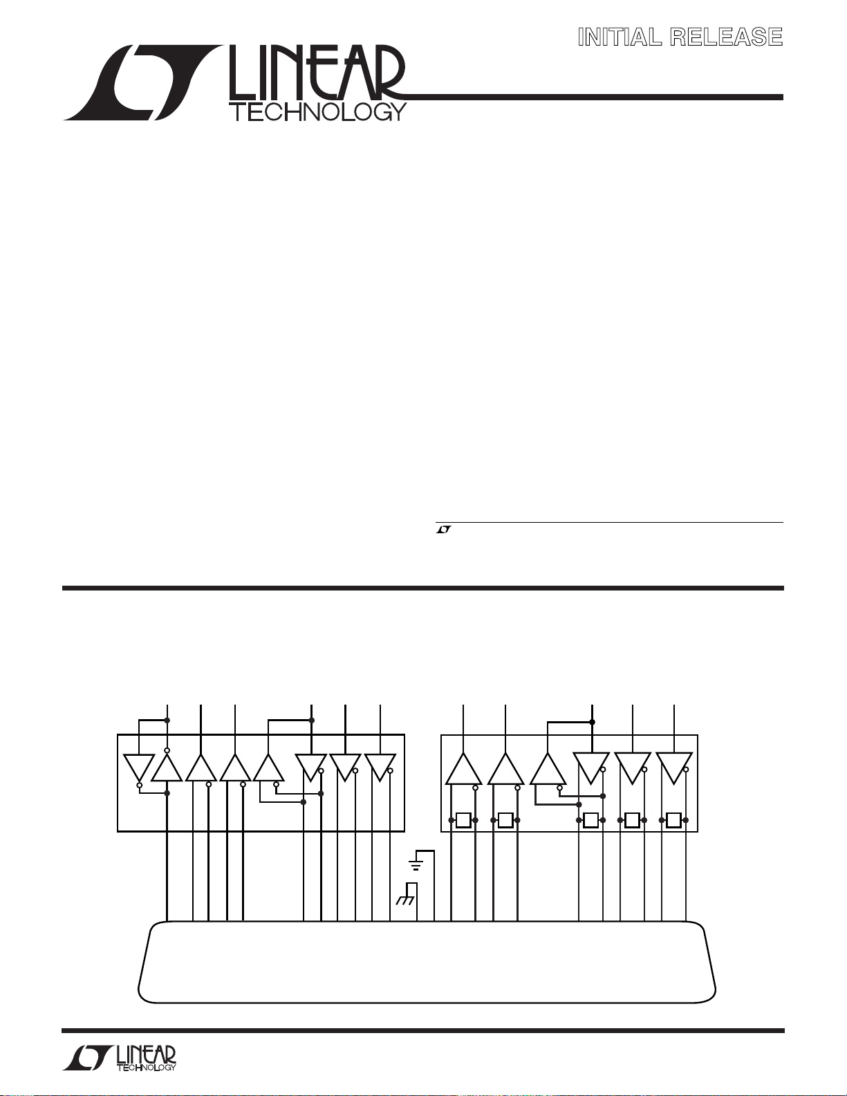
TYPICAL APPLICATIO
Complete DTE or DCE Multiprotocol Serial Interface with DB-25 Connector
LL
D4
R2 R1R4
R3
U
LTC1544
D3
DTRDSR DCDCTS
D2 D1
RTS
The LTC1546 runs from a single 5V supply using an internal
charge pump that requires only five space-saving surface
mounted capacitors. The LTC1546 is available in a 28-lead
SSOP surface mount package.
, LTC and LT are registered trademarks of Linear Technology Corporation.
RXCRXD
LTC1546
R1R2R3
TXDSCTETXC
D1
D2D3
TTTTT
CTS B
LL A (141)
DSR A (109)
DSR B
CTS A (106)
Information furnished by Linear Technology Corporation is believed to be accurate and reliable.
However, no responsibility is assumed for its use. Linear Technology Corporation makes no representation that the interconnection of its circuits as described herein will not infringe on existing patent rights.
DCD A (107)
DCD B
DTR B
RTS A (105)
RTS B
DTR A (108)
SG (102)
SHIELD (101)
RXD B
DB-25 CONNECTOR
RXC B
RXD A (104)
RXC A (115)
TXC B
TXC A (114)
SCTE B
SCTE A (113)
TXD B
21424111512179314192062322513 81018 7 16
TXD A (103)
1546 TA01
1
LTC1546
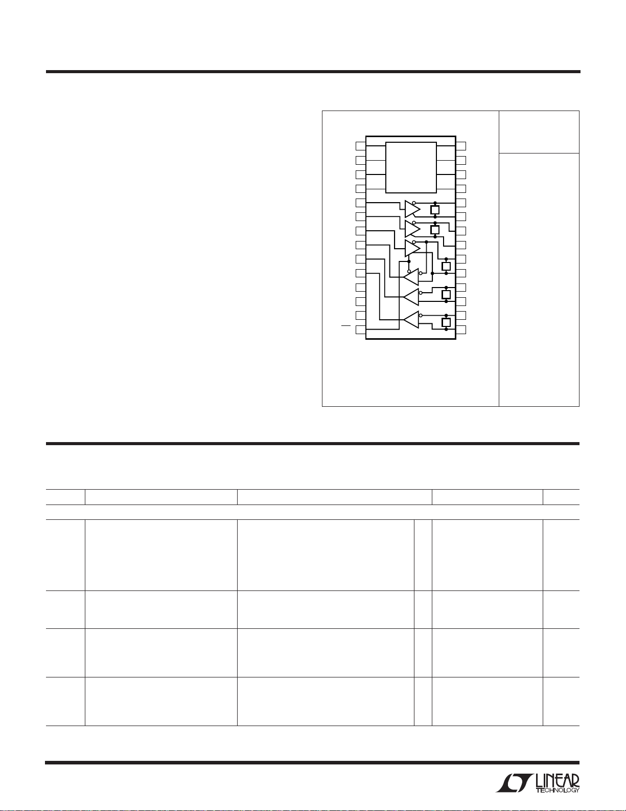
PACKAGE/ORDER I FOR ATIO
UU
W
WWWU
ABSOLUTE AXI U RATI GS
(Note 1)
Supply Voltage ....................................................... 6.5V
Input Voltage
Transmitters ........................... –0.3V to (VCC + 0.3V)
Receivers............................................... –18V to 18V
Logic Pins .............................. –0.3V to (VCC + 0.3V)
Output Voltage
Transmitters ................. (VEE – 0.3V) to (VDD + 0.3V)
Receivers................................ –0.3V to (VCC + 0.3V)
VEE........................................................ –10V to 0.3V
VDD....................................................... –0.3V to 10V
Short-Circuit Duration
Transmitter Output ..................................... Indefinite
Receiver Output.......................................... Indefinite
VEE.................................................................. 30 sec
Operating Temperature Range
LTC1546C ............................................... 0°C to 70°C
LTC1546I........................................... –40°C to 85°C
Storage Temperature Range ................ –65°C to 150°C
Lead Temperature (Soldering, 10 sec)................. 300°C
TOP VIEW
–
1
C1
+
2
C1
3
V
DD
4
V
CC
5
D1
6
D2
7
D3
8
R1
9
R2
10
R3
11
M0
12
M1
13
M2
14
DCE/DTE
*θJA SOLDERED TO A TYPICAL CIRCUIT BOARD
IS TYPICALLY 60°C/W
CHARGE PUMP
D1
D2
D3
R1
R2
R3
G PACKAGE
28-LEAD PLASTIC SSOP
T
= 150°C, θJA = 90°C/W*
JMAX
T
T
ORDER PART
+
C2
28
–
C2
27
V
26
EE
GND
25
D1 A
24
D1 B
23
D2 A
22
D2 B
21
D3/R1 A
20
T
D3/R1 B
19
R2 A
18
T
R2 B
17
R3 A
16
T
R3 B
15
NUMBER
LTC1546CG
LTC1546IG
Consult factory for Military grade parts.
ELECTRICAL CHARACTERISTICS
The ● denotes specifications which apply over the full operating
temperature range, otherwise specifications are at TA = 25°C. VCC = 5V (Notes 2, 3)
SYMBOL PARAMETER CONDITIONS MIN TYP MAX UNITS
Supplies
I
CC
P
D
+
V
–
V
VCC Supply Current (DCE Mode, RS530, RS530-A, X.21 Modes, No Load 14 mA
All Digital Pins = GND or V
) RS530, RS530-A, X.21 Modes, Full Load ● 100 130 mA
CC
V.35 Mode
● 126 170 mA
V.28 Mode, No Load 20 mA
V.28 Mode, Full Load ● 35 75 mA
No-Cable Mode
● 60 500 µA
Internal Power Dissipation (DCE Mode) RS530, RS530-A, X.21 Modes, Full Load 410 mW
V.35 Mode, Full Load 625 mW
V.28 Mode, Full Load 150 mW
Positive Charge Pump Output Voltage V.11 or V.28 Mode, No Load ● 8.0 9.3 V
V.35 Mode
V.28 Mode, with Load
V.28 Mode, with Load, I
= 10mA 6.5 V
DD
● 7.0 8.0 V
● 8.0 8.7 V
Negative Charge Pump Output Voltage V.28 Mode, No Load –9.6 V
V.28 Mode, Full Load
V.35 Mode
RS530, RS530-A, X.21 Modes, Full Load
● – 7.5 –8.5 V
● – 5.5 –6.5 V
● – 4.5 –6.0 V
2
LTC1546
ELECTRICAL CHARACTERISTICS
The ● denotes specifications which apply over the full operating
temperature range, otherwise specifications are at TA = 25°C. VCC = 5V (Notes 2, 3)
SYMBOL PARAMETER CONDITIONS MIN TYP MAX UNITS
f
OSC
t
r
Logic Inputs and Outputs
V
IH
V
IL
I
IN
V
OH
V
OL
I
OSR
I
OZR
V.11 Driver
V
ODO
V
ODL
∆V
OD
V
OC
∆V
OC
I
SS
I
OZ
tr, t
f
t
PLH
t
PHL
∆t Input to Output Difference, t
t
SKEW
V.11 Receiver
V
TH
∆V
TH
R
IN
tr, t
f
t
PLH
t
PHL
∆t Input to Output Difference, t
V.35 Driver
V
OD
VOA, V
V
OC
Charge Pump Oscillator Frequency 500 kHz
Charge Pump Rise Time No-Cable Mode/Power-Off to Normal Operation 2 ms
Logic Input High Voltage ● 2V
Logic Input Low Voltage ● 0.8 V
Logic Input Current D1, D2, D3 ● ±10 µA
M0, M1, M2, DCE = GND
M0, M1, M2, DCE = V
CC
● –120 –75 – 30 µA
● ±10 µA
Output High Voltage IO = –3mA ● 3 4.5 V
Output Low Voltage IO = 3mA ● 0.3 0.45 V
Output Short-Circuit Current 0V ≤ VO ≤ V
CC
Three-State Output Current M0 = M1 = M2 = VCC, 0V ≤ VO ≤ V
CC
● –50 50 mA
±1 µA
Open Circuit Differential Output Voltage RL = 1.95k (Figure 1) ● ±5V
Loaded Differential Output Voltage RL = 50Ω (Figure 1) 0.5V
= 50Ω (Figure 1) ● ±2V
R
L
ODO
0.67V
ODO
Change in Magnitude of Differential RL = 50Ω (Figure 1) ● 0.2 V
Output Voltage
Common Mode Output Voltage RL = 50Ω (Figure 1) ● 3V
Change in Magnitude of Common Mode RL = 50Ω (Figure 1) ● 0.2 V
Output Voltage
Short-Circuit Current V
Output Leakage Current V
= GND ±150 mA
OUT
and VB ≤ 0.25V, Power Off or ● ±1 ±100 µA
A
No-Cable Mode or Driver Disabled
Rise or Fall Time (Figures 2, 13) ● 21525 ns
Input to Output Rising (Figures 2, 13) ● 15 40 65 ns
Input to Output Falling (Figures 2, 13) ● 15 40 65 ns
– t
PLH
(Figures 2, 13) ● 0312 ns
PHL
Output to Output Skew (Figures 2, 13) 3 ns
Input Threshold Voltage –7V ≤ VCM ≤ 7V ● –0.2 0.2 V
Input Hysteresis –7V ≤ VCM ≤ 7V ● 15 40 mV
Input Impedance –7V ≤ VCM ≤ 7V (Figure 3) ● 100 103 Ω
Rise or Fall Time CL = 50pF (Figures 4, 14) 15 ns
Input to Output Rising CL = 50pF (Figures 4, 14) ● 50 90 ns
Input to Output Falling CL = 50pF (Figures 4, 14) ● 50 90 ns
– t
C
PLH
PHL
= 50pF (Figures 4, 14) ● 0425 ns
L
Differential Output Voltage Open Circuit, RL = 1.95k (Figure 5) ● ±1.2 V
With Load, –4V ≤ V
Single-Ended Output Voltage Open Circuit, RL = 1.95k (Figure 5) ● ±1.2 V
OB
≤ 4V (Figure 6) ±0.44 ±0.55 ±0.66 V
CM
Transmitter Output Offset RL = 50Ω (Figure 5) ● ±0.6 V
V
3
LTC1546
ELECTRICAL CHARACTERISTICS
The ● denotes specifications which apply over the full operating
temperature range, otherwise specifications are at TA = 25°C. VCC = 5V (Notes 2, 3)
SYMBOL PARAMETER CONDITIONS MIN TYP MAX UNITS
I
OH
I
OL
I
OZ
R
OD
R
OC
tr, t
f
t
PLH
t
PHL
∆t Input to Output Difference, t
t
SKEW
V.35 Receiver
V
TH
∆V
TH
R
ID
R
IC
tr, t
f
t
PLH
t
PHL
∆t Input to Output Difference, t
V.28 Driver
V
O
I
SS
R
OZ
SR Slew Rate RL = 7k, CL = 0 (Figures 11, 15) ● 430V/µs
t
PLH
t
PHL
V.28 Receiver
V
THL
V
TLH
∆V
TH
R
IN
tr, t
f
t
PLH
t
PHL
Transmitter Output High Current VA, VB = 0V ● – 13 –11 – 9.0 mA
Transmitter Output Low Current VA, VB = 0V ● 9.0 11 13 mA
Transmitter Output Leakage Current V
and VB ≤ 0.25V ● ±1 ±100 µA
A
Transmitter Differential Mode Impedance ● 50 100 150 Ω
Transmitter Common Mode Impedance – 2V ≤ VCM ≤ 2V (Figure 7) 135 150 165 Ω
Rise or Fall Time (Figures 8, 13) 5 ns
Input to Output (Figures 8, 13) ● 15 35 65 ns
Input to Output (Figures 8, 13) ● 15 35 65 ns
– t
PLH
(Figures 8, 13) ● 016 ns
PHL
Output to Output Skew (Figures 8, 13) 4 ns
Differential Receiver Input Threshold Voltage –2V ≤ VCM ≤ 2V (Figure 9) ● –0.2 0.2 V
Receiver Input Hysteresis –2V ≤ VCM ≤ 2V (Figure 9) ● 15 40 mV
Receiver Differential Mode Impedance –2V ≤ VCM ≤ 2V ● 90 103 110 Ω
Receiver Common Mode Impedance –2V ≤ VCM ≤ 2V (Figure 10) 135 150 165 Ω
Rise or Fall Time CL = 50pF (Figures 4, 14) 15 ns
Input to Output CL = 50pF (Figures 4, 14) ● 50 90 ns
Input to Output CL = 50pF (Figures 4, 14) ● 50 90 ns
– t
PLH
C
PHL
= 50pF (Figures 4, 14) ● 0425 ns
L
Output Voltage Open Circuit ● ±10 V
= 3k (Figure 11) ● ±5 ±8.5 V
R
L
Short-Circuit Current V
= GND ● ±150 mA
OUT
Power-Off Resistance –2V < VO < 2V, Power Off ● 300 Ω
or No-Cable Mode
Input to Output RL = 3k, CL = 2500pF (Figures 11, 15) ● 1.5 2.5 µs
Input to Output RL = 3k, CL = 2500pF (Figures 11, 15) ● 1.5 2.5 µs
Input Low Threshold Voltage (Figure 12) ● 1.2 0.8 V
Input High Threshold Voltage (Figure 12) ● 2 1.2 V
Receiver Input Hysteresis (Figure 12) ● 0 0.05 0.3 V
Receiver Input Impedance – 15V ≤ VA ≤ 15V ● 357 kΩ
Rise or Fall Time CL = 50pF (Figures 12, 16) 15 ns
Input to Output CL = 50pF (Figures 12, 16) ● 60 300 ns
Input to Output CL = 50pF (Figures 12, 16) ● 160 300 ns
Note 1: Absolute Maximum Ratings are those values beyond which the life
of the device may be impaired.
Note 2: All currents into device pins are positive; all currents out of device
are negative. All voltages are referenced to device ground unless otherwise
specified.
4
Note 3: All typicals are given for V
= 3.3µF and TA = 25°C.
C
VEE
= 5V, C1 = C2 = C
CC
VCC
= C
VDD
= 1µF,

LTC1546
U
UU
PI FU CTIO S
C1–␣ (Pin 1): Capacitor C1 Negative Terminal. Connect a
1µF capacitor between C1+ and C1–.
C1+ (Pin 2): Capacitor C1 Positive Terminal. Connect a
1µF capacitor between C1+ and C1–.
VDD (Pin 3): Generated Positive Supply Voltage for
V.28. Connect a 1µF capacitor to ground.
VCC (Pin 4): Positive Supply Voltage Input. 4.75V ≤ V
≤ 5.25V. Bypass with a 1µF capacitor to ground.
D1 (Pin 5): TTL Level Driver 1 Input.
D2 (Pin 6): TTL Level Driver 2 Input.
D3 (Pin 7): TTL Level Driver 3 Input.
R1 (Pin 8): CMOS Level Receiver 1 Output.
R2 (Pin 9): CMOS Level Receiver 2 Output.
R3 (Pin 10): CMOS Level Receiver 3 Output.
M0 (Pin 11): TTL Level Mode Select Input 0 with Pull-Up
to VCC. See Table 1.
M1 (Pin 12): TTL Level Mode Select Input 1 with Pull-Up
to VCC. See Table 1.
M2 (Pin 13): TTL Level Mode Select Input 2 with Pull-Up
to VCC. See Table 1.
CC
R3 B (Pin 15): Receiver 3 Noninverting Input.
R3 A (Pin 16): Receiver 3 Inverting Input.
R2 B (Pin 17): Receiver 2 Noninverting Input.
R2 A (Pin 18): Receiver 2 Inverting Input.
D3/R1 B (Pin 19): Receiver 1 Noninverting Input and
Driver 3 Noninverting Output.
D3/R1 A (Pin 20): Receiver 1 Inverting Input and Driver 3
Inverting Output.
D2 B (Pin 21): Driver 2 Noninverting Output.
D2 A (Pin 22): Driver 2 Inverting Output.
D1 B (Pin 23): Driver 1 Noninverting Output.
D1 A (Pin 24): Driver 1 Inverting Output.
GND (Pin 25): Ground.
VEE (Pin 26): Negative Supply Voltage. Connect a 3.3µF
capacitor to GND.
C2– (Pin 27): Capacitor C2 Negative Terminal. Connect a
1µF capacitor between C2+ and C2–.
C2+ (Pin 28): Capacitor C2 Positive Terminal. Connect a
1µF capacitor between C2+ and C2–.
DCE/DTE (Pin 14): TTL Level Mode Select Input with PullUp to VCC. See Table 1.
5
LTC1546
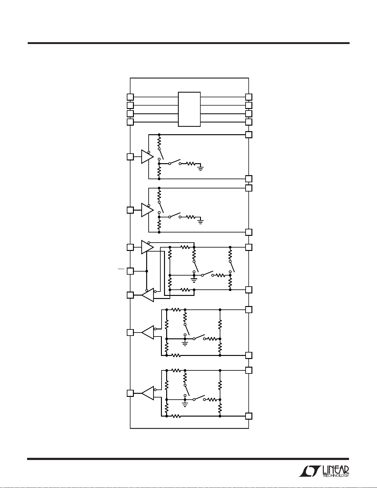
BLOCK DIAGRA
W
CHARGE
PUMP
–
C1
+
C1
2
V
3
DD
V
4
CC
50Ω
–
+
C1
C2
+
–
C1
C2
V
V
DD
EE
V
GND
CC
+
C2
281
–
C2
27
V
26
EE
GND
25
D1A
24
DCE/DTE
D1
D2
D3
R1
R2
D1
5
D2
6
D3
7
14
8
9
S1
S2
125Ω
50Ω
D1B
23
22
D2A
50Ω
S1
S2
125Ω
50Ω
D2B
21
20
19
18
D3/R1 A
D3/R1 B
R2A
20k
10k 6k
S3
S2
10k
20k
R1
20k
6k
10k
R2
S3
S2
125Ω
51.5Ω
S1
125Ω
51.5Ω
51.5Ω
6
10k
20k
20k
6k
10k
R3
10
R3
10k
20k
S3
S2
125Ω
51.5Ω
51.5Ω
51.5Ω
R2B
17
R3A
16
R3B
15
1546 BD
 Loading...