

Linear Technology LTC1536 Datasheet
FEATURES
■
Simultaneously Monitors 5V, 3.3V and
Adjustable Inputs
■
Guaranteed Threshold Accuracy: ±0.75%
■
Low Supply Current: 100µA
■
Internal Reset Time Delay: 200ms
■
Manual Pushbutton Reset Input
■
Active Low and Active High Reset Outputs
■
Active Low “Soft” Reset Output
■
Power Supply Glitch Immunity
■
Guaranteed Reset for Either V
■
Meets PCI t
■
8-Pin SO and MSOP Packages
Timing Specifications Rev 2.1
FAIL
≥ 1V or V
CC3
U
APPLICATIO S
■
PCI-Based Systems
■
Desktop Computers
■
Notebook Computers
■
Intelligent Instruments
■
Portable Battery-Powered Equipment
■
Network Servers
CC5
≥ 1V
LTC1536
Precision Triple Supply Monitor
for PCI Applications
U
DESCRIPTIO
The LTC®1536 is designed for PCI local bus applications
with multiple supply voltages that require low power,
small size, high speed and high accuracy supply
monitoring.
For 3.3V and 5V supplies that are >500mV below spec or
for the condition when the 5V supply falls below the 3.3V
supply, the LTC1536 has a very fast response time capable
of meeting the PCI t
threshold accuracy and glitch immunity ensure reliable
reset operation without false triggering.
The RST output is guaranteed to be in the correct state for
V
CC5
or V
down to 1V. The 100µA typical supply current
CC3
makes the LTC1536 ideal for power-conscious systems.
A manual pushbutton reset input provides the ability to
generate a very narrow “soft” reset pulse (100µs typ) or a
200ms reset pulse equivalent to a power-on reset. Both
SRST and RST outputs are open-drain and can be OR-tied
with other reset sources.
, LTC and LT are registered trademarks of Linear Technology Corporation.
timing specification. Tight 0.75%
FAIL
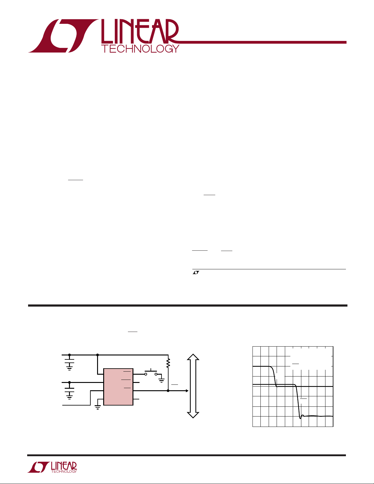
TYPICAL APPLICATIO
Motherboard PCI RST Generation
3.3V ±0.3V
5V ±5%
PWR GOOD
0.1µF
0.1µF
LTC1536
1
V
CC3
2
V
CC5
3
V
CCA
4
GND
SELECTED TO MEET RISE TIME
R
PU
SLEW RATE REQUIREMENTS (1k MIN)
U
PBR
SRST
RST
RST
PUSHBUTTON
RESET
8
7
6
5
R
RST
Power Fail Waveform
5V Dropping Below 3.3V by 300mV
V
= 5V TO 3V STEP
CC5
= V
RST
CCA
= 3.3V
CC3
1536 TA02
V
CC3
PU
PCI
LOCAL
BUS
1536 TA01
5
4
3
2
VOLTAGE (1V/DIV)
1
0
4.7k PULL-UP FROM
RST TO V
V
CC5
TIME (20ns/DIV)
1
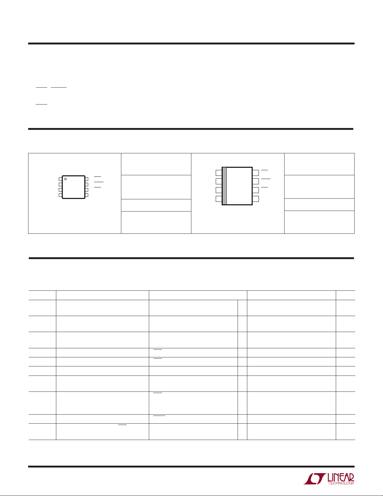
LTC1536
1
2
3
4
8
7
6
5
TOP VIEW
S8 PACKAGE
8-LEAD PLASTIC SO
V
CC3
V
CC5
V
CCA
GND
PBR
SRST
RST
RST
1
2
3
4
V
CC3
V
CC5
V
CCA
GND
8
7
6
5
PBR
SRST
RST
RST
TOP VIEW
MS8 PACKAGE
8-LEAD PLASTIC MSOP
A
W
O
LUTEXI TIS
S
A
WUW
U
ARB
G
(Notes 1, 2)
Terminal Voltage
V
, V
, V
CC3
CC5
.................................... –0.3V to 7V
CCA
RST, SRST ............................................ –0.3V to 7V
RST ......................................... –0.3V to V
CC3
+ 0.3V
PBR .......................................................... –7V to 7V
WU
/
= 125°C, θ
O
RDER I FOR ATIO
ORDER
PART NUMBER
LTC1536CMS8
MS8 PART MARKING
= 160°C/W
JA
LTBV
PACKAGE
T
JMAX
Operating Temperature Range
LTC1536C .............................................. 0°C to 70°C
LTC1536I............................................ –40°C to 85°C
Storage Temperature Range ................ –65°C to 150°C
Lead Temperature (Soldering, 10 sec)................. 300°C
U
ORDER
PART NUMBER
LTC1536CS8
LTC1536IS8
S8 PART MARKING
T
JMAX
= 125°C, θ
= 150°C/W
JA
1536
1536I
Consult factory for Military grade parts.
ELECTRICAL CHARACTERISTICS
V
= 3.3V, V
CC3
SYMBOL PARAMETER CONDITIONS MIN TYP MAX UNITS
V
RT3
V
RT5
V
RTA
V
CC
I
VCC3
I
VCC5
I
VCCA
t
RST
t
SRST
t
UV
2
= 5V, V
CC5
Reset Threshold V
Reset Threshold V
Reset Threshold V
V
or V
CC3
V
Supply Current PBR = V
CC3
V
Input Current V
CC5
V
Input Current V
CCA
Reset Pulse Width RST Low with 10kΩ Pull-Up to V
Soft Reset Pulse Width SRST Low with 10kΩ Pull-Up to V
VCC Undervoltage Detect to RST V
= V
CCA
Operating Voltage RST in Correct Logic State ● 17V
CC5
, TA = 25°C unless otherwise noted.
CC3
CC3
CC5
CCA
0°C ≤ TA ≤ 70°C ● 2.962 2.985 3.000 V
–40°C ≤ T
0°C ≤ TA ≤ 70°C ● 4.687 4.725 4.750 V
–40°C ≤ T
0°C ≤ TA ≤ 70°C ● 0.992 1.000 1.007 V
–40°C ≤ T
= 5V ● 10 20 µA
CC5
= 1V, 0°C ≤ TA ≤ 70°C ● –5 0 5 nA
CCA
V
= 1V, –40°C ≤ TA ≤ 85°C ● –15 0 15 nA
CCA
0°C to 70°C ● 140 200 280 ms
–40°C to 85°C
, V
CC5
Threshold V
≤ 85°C ● 2.925 2.985 3.008 V
A
≤ 85°C ● 4.625 4.725 4.762 V
A
≤ 85°C ● 0.980 1.000 1.007 V
A
CC3
or V
CC3
Less Than Reset 13 µs
CCA
by 1%
RT
● 100 200 µA
CC3
● 140 200 300 ms
● 50 100 200 µs
CC3
LTC1536
ELECTRICAL CHARACTERISTICS
V
= 3.3V, V
CC3
SYMBOL PARAMETER CONDITIONS MIN TYP MAX UNITS
I
PBR
V
IL
V
IH
t
PW
t
DB
t
PB
V
OL
V
OH
t
PHL
t
PLH
t
FAIL
t
PF
= 5V, V
CC5
CCA
= V
, TA = 25°C unless otherwise noted.
CC3
PBR Pull-Up Current PBR = 0V, 0°C ≤ TA ≤ 70°C ● 3710 µA
PBR = 0V, –40°C ≤ T
≤ 85°C ● 3715 µA
A
PBR, RST Input Low Voltage ● 0.8 V
PBR, RST Input High Voltage ● 2V
PBR Min Pulse Width ● 40 ns
PBR Debounce Deassertion of PBR Input to SRST ● 20 35 ms
Output (PBR Pulse Width = 1µs)
PBR Assertion Time for Transition PBR Held Less Than VIL, 0°C to 70°C ● 1.4 2.0 2.8 s
from Soft to Hard Reset Mode PBR Held Less Than V
RST Output Voltage Low I
SRST Output Voltage Low I
RST Output Voltage Low I
RST Output Voltage High (Note 3) I
SRST Output Voltage High (Note 3) I
RST Output Voltage High I
Propagation Delay RST to RST C
= 5mA ● 0.15 0.4 V
SINK
I
= 100µAV
SINK
≤ 70°CV
0°C ≤ T
A
I
= 100µAV
SINK
–40°C ≤ T
SINK
SINK
SOURCE
SOURCE
SOURCE
RST
≤ 85°CV
A
= 2.5mA ● 0.15 0.4 V
= 2.5mA ● 0.15 0.4 V
= 1µA ● V
= 1µA ● V
= 600µA ● V
= 20pF 25 ns
, –40°C to 85°C ● 1.4 2.0 3.0 s
IL
CC3
CC3
V
CC3
CC3
CC3
V
CC3
= 1V, V
= 0V, V
= 1V, V
= 1.1V, V
= 0V, V
= 1.1V, V
= 0V ● 0.05 0.4 V
CC5
= 1V ● 0.05 0.4 V
CC5
= 1V ● 0.05 0.4 V
CC5
= 0V ● 0.05 0.4 V
CC5
= 1.1V ● 0.05 0.4 V
CC5
= 1.1V ● 0.05 0.4 V
CC5
– 1 V
CC3
– 1 V
CC3
– 1 V
CC3
High Input to Low Output
Propagation Delay RST to RST C
= 20pF 45 ns
RST
Low Input to High Output
V
or V
CC5
0.5V Undervoltage V
CC3
Drops Below 4.25V or V
CC5
Drops ● 150 450 ns
CC3
to RST (Note 4) Below 2.5V (Note 5)
V
< (V
CC5
– 300mV) RST (Note 4) V
CC3
Drops Below V
CC5
By 300mV ● 50 90 ns
CC3
(Note 6)
● denotes specifications which apply over the full operating
The
temperature range.
Note 1: Absolute Maximum Ratings are those values beyond which the life
of the device may be impaired.
Note 2: All voltage values are with respect to GND.
Note 3: The output pins SRST and RST have weak internal pull-ups to
V
of 6µA. However, external pull-up resistors may be used when faster
CC3
rise times are required.
Note 4: Conforms to PCI Local Bus Specification Rev 2.1,
Sect. 4.3.2 for t
Note 5: V
V
Note 6: V
V
CC3
– 500mV to RST at 1.5V.
RTX
CC5
= (V
CC5
CC3
.
FAIL
or V
falling at –0.1V/µs, time measured from
CC5
falling from 5V to 3V in ≤10ns, time measured from
– 300mV) to RST at 1.5V.
3
LTC1536
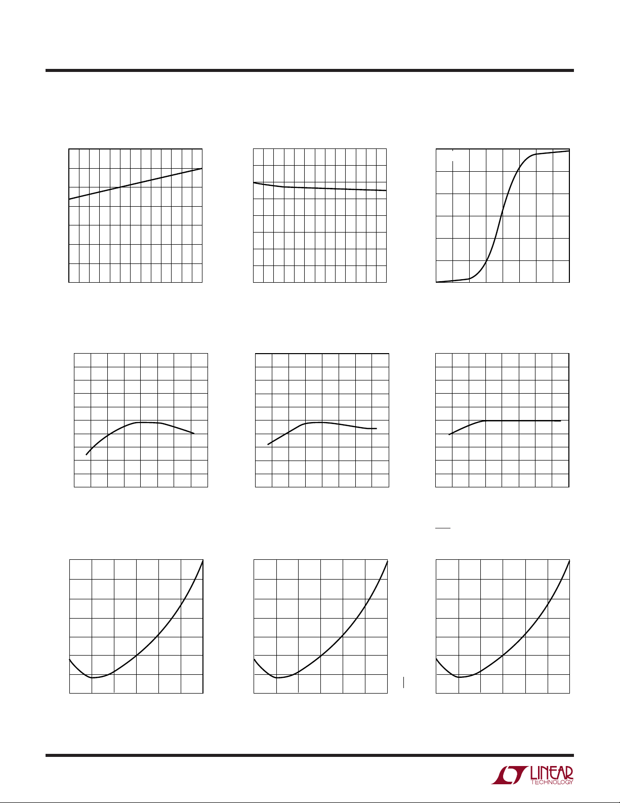
INPUT VOLTAGE (V)
0.8
–3
INPUT CURRENT (nA)
–2
–1
0
1
0.9 1.0
1.1
1.2
1536 G03
2
3
0.85 0.95
1.05
1.15
TA = 25°C
UW
TYPICAL PERFORMANCE CHARACTERISTICS
I
vs Temperature
VCC3
140
120
100
80
(µA)
60
VCC3
I
40
20
0
–45
V
–5
–25
TEMPERATURE (°C)
Threshold Voltage
CC5
vs Temperature
4.750
4.745
(V)
4.740
RT5
4.735
4.730
4.725
4.720
4.715
THRESHOLD VOLTAGE, V
4.710
CC5
V
4.705
4.700
–60
–40 0
–20
TEMPERATURE (°C)
35
15
20
55
75
1536 G01
80
60
40
100
1536 G04
I
vs Temperature
VCC5
20.0
17.5
15.0
12.5
(µA)
10.0
VCC5
I
7.5
5.0
2.5
0
–45
V
CC3
–5
–25
TEMPERATURE (°C)
Threshold Voltage
vs Temperature
3.010
3.005
(V)
3.000
RT3
2.995
2.990
2.985
2.980
2.975
THRESHOLD VOLTAGE, V
2.970
CC3
V
2.965
2.960
–60
–20 20
–40 80
TEMPERATURE (°C)
35
15
0 40 100
55
60
75
1536 G02
1536 G05
V
Input Current
CCA
vs Input Voltage
V
Threshold Voltage
CCA
vs Temperature
1.005
1.004
(V)
1.003
RTA
1.002
1.001
1.000
0.999
0.998
THRESHOLD VOLTAGE, V
0.997
CCA
V
0.996
0.995
–60
–40 0
–20
TEMPERATURE (°C)
80
20
60
40
100
1536 G06
225
220
(ms)
215
RST
210
205
200
RESET PULSE WIDTH, t
195
190
4
Reset Pulse Width
vs Temperature
–50
–25 0
TEMPERATURE (°C)
50 100
25 75
1536 G07
“Soft” Reset Pulse Width
vs Temperature
112.5
110.0
(µs)
SRST
107.5
105.0
102.5
100.0
97.5
SOFT RESET PULSE WIDTH, t
95.0
–50
–25 0
TEMPERATURE (°C)
50 100
25 75
1536 G08
PBR Assertion Time to Reset
vs Temperature
2.25
(SEC)
2.20
PB
2.15
2.10
2.05
2.00
1.95
PBR ASSERTION TIME TO RESET, t
1.90
–50
–25 0
25 75
TEMPERATURE (°C)
50 100
1536 G09
 Loading...