

Linear Technology LTC1446, LTC1446L Datasheet
LTC1446/LTC1446L
Dual 12-Bit Rail-to-Rail
Micropower DACs in SO-8
EATU
F
■
Dual DACs with 12-Bit Resolution
■
SO-8 Package
■
Rail-to-Rail Output Amplifiers
■
3V Operation (LTC1446L): ICC = 650µA Typ
■
5V Operation (LTC1446): ICC = 1000µA Typ
■
Internal Reference
■
Power-On Reset Clears DACs to 0V
■
3-Wire Cascadable Serial Interface
■
Maximum DNL Error: 0.5LSB
■
Low Cost
■
Schmitt Trigger On Input Allows Direct
RE
S
Optocoupler Interface
U
O
PPLICATI
A
■
Digital Calibration
■
Industrial Process Control
■
Automatic Test Equipment
■
Cellular Telephones
S
DUESCRIPTIO
The LTC®1446/LTC1446L are dual 12-bit digital-to-analog
converters (DACs) available in an SO-8 package. They are
complete with a rail-to-rail voltage
internal reference and an easy-to-use 3-wire cascadable
serial interface.
The LTC1446 has an internal reference and a full-scale
output of 4.095V. It operates from a single 4.5V to 5.5V
supply.
The LTC1446L has an internal reference and a full-scale
output of 2.5V. It operates from a single 2.7V to 5.5V
supply.
The low power supply current makes the LTC1446 family
ideal for battery-powered applications. These DACs are
available in space saving 8-pin SO and PDIP packages and
require no external components for operation.
, LTC and LT are registered trademarks of Linear Technology Corporation.
output amplifier, an
U
O
A
PPLICATITYPICAL
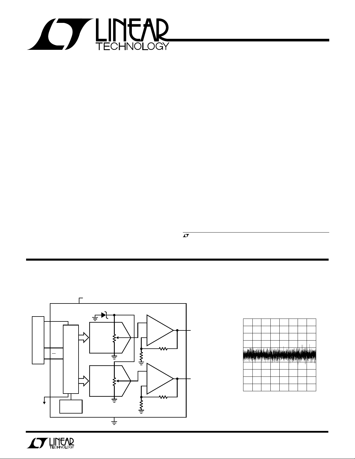
Functional Block Diagram: Dual 12-Bit Rail-to-Rail DAC
LTC1446: 5V
LTC1446L: 3V TO 5V
7
V
CC
DIN2
µP
CLK1
24-BIT
SHIFT
CS/LD3
REG
AND
DAC
LATCH
4
D
OUT
POWER-ON
RESET
12-BIT
DAC B
12-BIT
DAC A
GND
6
+
–
+
–
V
OUT B
V
OUT A
1446/1446L TA01
8
RAIL-TO-RAIL
VOLTAGE
OUTPUT
5
Differential Nonlinearity vs Input Code
0.5
0.4
0.3
0.2
0.1
0
–0.1
DNL ERROR (LSB)
–0.2
–0.3
–0.4
–0.5
1024 2048 2560
512 1536 3072 3584 4095
0
CODE
1446/46L G13
1
LTC1446/LTC1446L
A
W
O
LUTEXI T
S
A
WUW
ARB
U
G
I
S
VCC to GND................................................ –0.5 to 7.5V
Logic Inputs to GND................................... –0.5 to 7.5V
Operating Temperature Range
LTC1446C/LTC1446LC............................0°C to 70°C
LTC1446I/LTC1446LI ..........................–40°C to 85°C
U
W
PACKAGE/ORDER INFORMATION
ORDER PART
TOP VIEW
1
CLK
D
2
IN
CS/LD
3
D
4
OUT
N8 PACKAGE
8-LEAD PDIP
T
= 125°C, θJA = 100°C/W
JMAX
Consult factory for Military grade parts.
V
8
OUT B
V
7
CC
GND
6
V
5
OUT A
NUMBER
LTC1446CN8
LTC1446IN8
LTC1446LCN8
LTC1446LIN8
V
OUT A/VOUT B
.................................–0.5V to VCC + 0.5V
Maximum Junction Temperature..........................125°C
Storage Temperature Range ..................–65°C to 150°C
Lead Temperature (Soldering, 10 sec)................. 300°C
U
ORDER PART
NUMBER
LTC1446CS8
LTC1446IS8
LTC1446LCS8
LTC1446LIS8
S8 PART MARKING
1446C 1446LC
1446I 1446LI
1
CLK
D
2
IN
CS/LD
3
D
4
OUT
8-LEAD PLASTIC SO
= 125°C, θJA = 150°C/W
T
JMAX
TOP VIEW
S8 PACKAGE
V
8
OUT B
V
7
CC
GND
6
V
5
OUT A
ELECTRICAL CHARACTERISTICS
VCC = 4.5V to 5.5V (LTC1446), 2.7V to 5.5V (LTC1446L), V
SYMBOL PARAMETER CONDITIONS MIN TYP MAX UNITS
DAC
Resolution ● 12 Bits
DNL Differential Nonlinearity Guaranteed Monotonic (Note 1) ● ±0.2 ±0.5 LSB
INL Integral Nonlinearity TA = 25°C ±2.0 4.5 LSB
ZSE Zero-Scale Error ● 0 3 18 mV
V
OS
V
TC Offset Error Tempco ±15 µV/°C
OS
V
FS
V
TC Full-Scale Voltage Tempco ±0.1 LSB/°C
FS
Power Supply (LTC1446)
V
CC
I
CC
Power Supply (LTC1446L)
V
CC
I
CC
Offset Error ● ±2 ±18 mV
Full-Scale Voltage LTC1446, TA = 25°C 4.065 4.095 4.125 V
LTC1446 ● 4.045 4.095 4.145 V
LTC1446L, T
LTC1446L ● 2.460 2.500 2.540 V
Positive Supply Voltage For Specified Performance ● 4.5 5.5 V
Supply Current 4.5V ≤ V
Positive Supply Voltage For Specified Performance ● 2.7 5.5 V
Supply Current 2.7V ≤ V
and V
OUT A
= 25°C 2.470 2.500 2.530 V
A
≤ 5.5V (Note 4) ● 1000 1500 µA
CC
≤ 5.5V (Note 4) ● 650 1000 µA
CC
unloaded, TA = T
OUT B
to T
MIN
● ±2.5 5.0 LSB
unless otherwise noted.
MAX,
2
LTC1446/LTC1446L
ELECTRICAL CHARACTERISTICS
VCC = 4.5V to 5.5V (LTC1446), 2.7V to 5.5V (LTC1446L), V
SYMBOL PARAMETER CONDITIONS MIN TYP MAX UNITS
Op Amp DC Performance
Short-Circuit Current Low V
Short-Circuit Current High V
Output Impedance to GND Input Code = 0 ● 40 120 Ω
AC Performance
Voltage Output Slew Rate (Note 2) ● 0.5 1 V/µs
Voltage Output Settling Time (Notes 2, 3) to ±0.5LSB 14 µs
OUT
OUT
and V
OUT A
Shorted to GND ● 55 120 mA
Shorted to V
unloaded, TA = T
OUT B
CC
to T
MIN
● 70 120 mA
unless otherwise noted.
MAX,
VCC = 5V (LTC1446), VCC = 3V (LTC1446L), TA = T
SYMBOL PARAMETER CONDITIONS MIN TYP MAX MIN TYP MAX UNITS
Digital I/O
V
IH
V
IL
V
OH
V
OL
I
LEAK
C
IN
Switching
t
1
t
2
t
3
t
4
t
5
t
6
t
7
t
8
t
9
Digital Input High Voltage ● 2.4 2 V
Digital Input Low Voltage ● 0.8 0.6 V
Digital Output High Voltage I
Digital Output Low Voltage I
Digital Input Leakage VIN = GND to V
Digital Input Capacitance Guaranteed by Design ● 10 10 pF
DIN Valid to CLK Setup ● 40 60 ns
DIN Valid to CLK Hold ● 00ns
CLK High Time ● 40 60 ns
CLK Low Time ● 40 60 ns
CS/LD Pulse Width ● 50 80 ns
LSB CLK to CS/LD ● 40 60 ns
CS/LD Low to CLK ● 20 30 ns
D
Output Delay C
OUT
CLK Low to CS/LD Low ● 20 30 ns
= –1mA ● VCC – 1.0 VCC – 0.7 V
OUT
= 1mA ● 0.4 0.4 V
OUT
= 15pF ● 150 220 ns
LOAD
MIN
to T
CC
unless otherwise noted.
MAX,
LTC1446 LTC1446L
● ±10 ±10 µA
The
● denotes specifications which apply over the full operating
temperature range.
Note 1: Nonlinearity is defined from the first code that is greater
than or equal to the maximum offset specification to code 4095
(full scale).
Note 2: Load is 5kΩ in parallel with 100pF.
Note 3: DAC switched between all 1s and the code corresponding
to VOS for the part.
Note 4: Digital inputs at 0V or VCC.
3
LTC1446/LTC1446L
CODE
0
–0.5
DNL ERROR (LSB)
–0.4
–0.2
–0.1
0
0.5
0.2
1024 2048 2560
1446/46L G03
–0.3
0.3
0.4
0.1
512 1536 3072 3584 4095
LOAD CURRENT (mA)
0
0
V
CC
– V
OUT
0.2
0.4
0.6
0.8
1.2
510
LTC1446/46L • TPC06
15
1.0
∆V
OUT
< 1LSB
CODE: ALL 1's
V
OUT
= 2.5V
LOGIC INPUT VOLTAGE (V)
0.6
SUPPLY CURRENT (mA)
1.4
2.2
3.0
1.0
1.8
2.6
1234
1446/46L G09
50
W
U
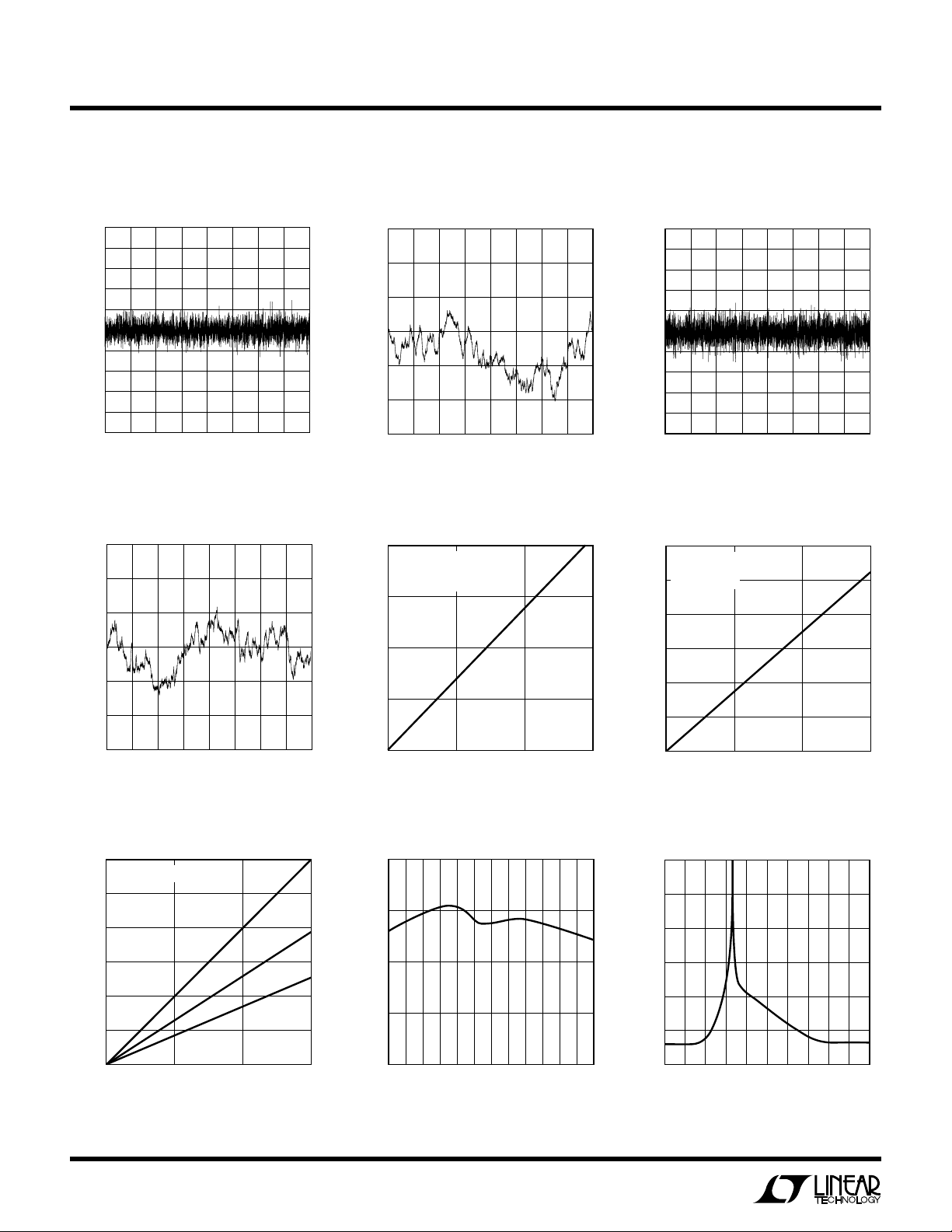
TYPICAL PERFORMANCE CHARACTERISTICS
LTC1446 Differential Nonlinearity
(DNL) LTC1446 Integral Nonlinearity (INL) LTC1446L Differential Nonlinearity
0.5
0.4
0.3
0.2
0.1
0
–0.1
DNL ERROR (LSB)
–0.2
–0.3
–0.4
–0.5
1024 2048 2560
512 1536 3072 3584 4095
0
CODE
1446/46L G01
3
2
1
0
–1
INL ERROR (LSB)
–2
–3
512 1536
0
1024 2048
CODE
2560
3072
3584
1446/46L G02
4095
LTC1446L Integral Nonlinearity
3
2
1
0
–1
INL ERROR (LSB)
–2
–3
512 1536
0
1024 2048
LTC1446 Min Output Voltage vs
Output Sink Current
600
CODE: ALL 0'S
500
400
300
200
100
OUTPUT PULL-DOWN VOLTAGE (mV)
0
0
OUTPUT SINK CURRENT (mA)
4
3072
2560
CODE
125°C
510
25°C
–55°C
LTC1446/46L • TPC07
3584
1446/46L G04
4095
15
LTC1446 Min Supply Headroom for
Full Output Swing vs Load Current
0.8
∆V
< 1LSB
OUT
CODE: ALL 1's
= 4.095V
V
OUT
0.6
(V)
OUT
0.4
– V
CC
V
0.2
0
0
5
LOAD CURRENT (mA)
10
LTC1446 Full-Scale Voltage
vs Temperature
4.11
4.10
4.09
4.08
FULL-SCALE VOLTAGE (V)
4.07
–55
–25 5 35 65
TEMPERATURE (°C)
LTC1446L Min Supply Headroom for
Full Output Swing vs Load Current
15
LTC1446/46L • TPC05
LTC1446 Supply Current
vs Logic Input Voltage
95 125
1446/46L G09
 Loading...