

FEATURES
LTC1440/LTC1441/LTC1442
Ultralow Power Single/Dual
Comparator with Reference
U
DESCRIPTIO
■
Ultralow Quiescent Current: 2.1µA Typ (LTC1440)
■
Reference Output Drives 0.01µF Capacitor
■
Adjustable Hysteresis (LTC1440/LTC1442)
■
Wide Supply Range:
Single: 2V to 11V
Dual: ± 1V to ± 5.5V
■
Input Voltage Range Includes the Negative Supply
■
TTL/CMOS Compatible Outputs
■
12µs Propagation Delay with 10mV Overdrive
■
No Crowbar Current
■
40mA Continuous Source Current
■
Pin Compatible Upgrades for MAX921/922/923
■
3mm x 3mm x 0.8mm DFN Package (LTC1440)
U
APPLICATIONS
■
Battery-Powered System Monitoring
■
Threshold Detectors
■
Window Comparators
■
Oscillator Circuits
, LTC and LT are registered trademarks of Linear Technology Corporation.
All other trademarks are the property of their respective owners.
The LTC®1440/LTC1441/LTC1442 are ultralow power
single and dual comparators with built-in references. The
comparators feature less than 3.7µA supply current over
temperature (LTC1440), a 1.182V ±1% reference, programmable hysteresis (LTC1440/LTC1442) and TTL/CMOS
outputs that sink and source current. The reference output
can drive a bypass capacitor of up to 0.01µF without
oscillation.
The comparators operate from a single 2V to 11V supply
or a dual ± 1V to ±5.5V supply (LTC1440). Comparator
hysteresis is easily programmed by using two resistors
and the HYST pin (LTC1440/LTC1442). Each comparator’s
input operates from the negative supply to within 1.3V of
the positive supply. The comparator output stage can
continuously source up to 40mA. By eliminating the
cross-conducting current that normally happens when the
comparator changes logic states, the power supply glitches
are eliminated.
The LTC1440 is available in 8-pin PDIP, SO, MSOP and
DFN packages. The LTC1441/LTC1442 are available in
8-pin PDIP and SO packages.
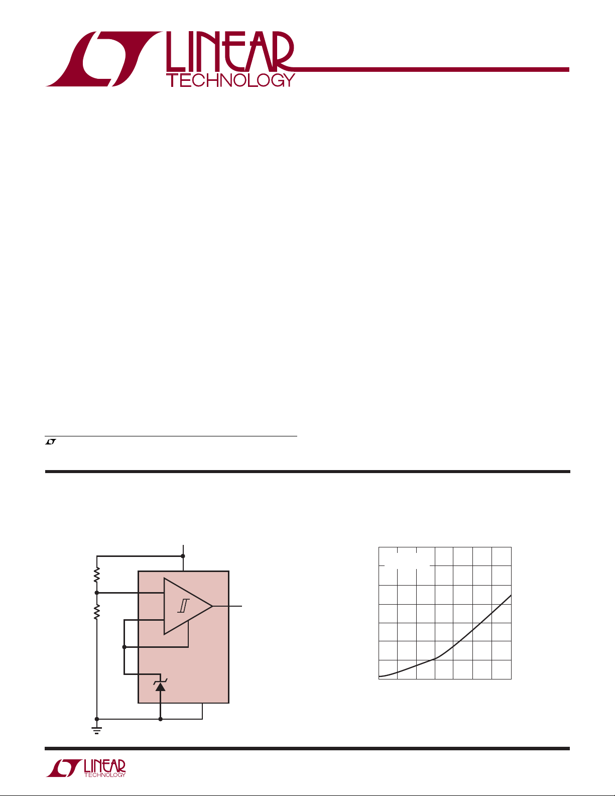
TYPICAL APPLICATIO
Micropower 2.9V VCC Threshold Detector
3.3V
R1
1.65M
1%
R2
1.13M
1%
+
IN
3
–
4
IN
5
HYST
6
REF
7
+
V
+
–
LTC1440
–
V
21
GND
U
1440 TA01
LTC1440 Supply Current vs Temperature
5.0
V+ = 5V
–
= GND = 0V
V
4.5
4.0
8
OUT
3.5
3.0
2.5
SUPPLY CURRENT (µA)
2.0
1.5
–40
–20 0
40 80
20 60
TEMPERATURE (°C)
100
1440/1/2 TA02
144012fb
1
LTC1440/LTC1441/LTC1442
WW
W
U
ABSOLUTE MAXIMUM RATINGS
(Note 1)
Voltage
+
V
to V–, V+ to GND, GND to V–...........12V to – 0.3V
+
, IN–, HYST ................. (V+ + 0.3V) to (V–– 0.3V)
IN
REF ................................... (V
OUT (LTC1440) .............. (V
+
+ 0.3V) to (V–– 0.3V)
+
+ 0.3V) to (GND – 0.3V)
OUT (LTC1441/LTC1442) ... (V+ + 0.3V) to (V–– 0.3V)
Current
+
IN
, IN–, HYST ................................................. 20mA
REF ................................................................... 20mA
OUT .................................................................. 50mA
OUT Short-Circuit Duration (V+ ≤ 5.5V) .......Continuous
Power Dissipation.............................................. 500mW
Operating Temperature Range
LTC144XC ............................................... 0°C to 70°C
LTC144XI ........................................... – 40°C to 85°C
Storage Temperature Range ................. –65°C to 150°C
Storage Temperature Range
(DD Package) ................................... – 65°C to 125°C
Junction Temperature........................................... 150°C
Junction Temperature (DD Package) .................... 125°C
Lead Temperature (Soldering, 10 sec).................. 300°C
U
W
U
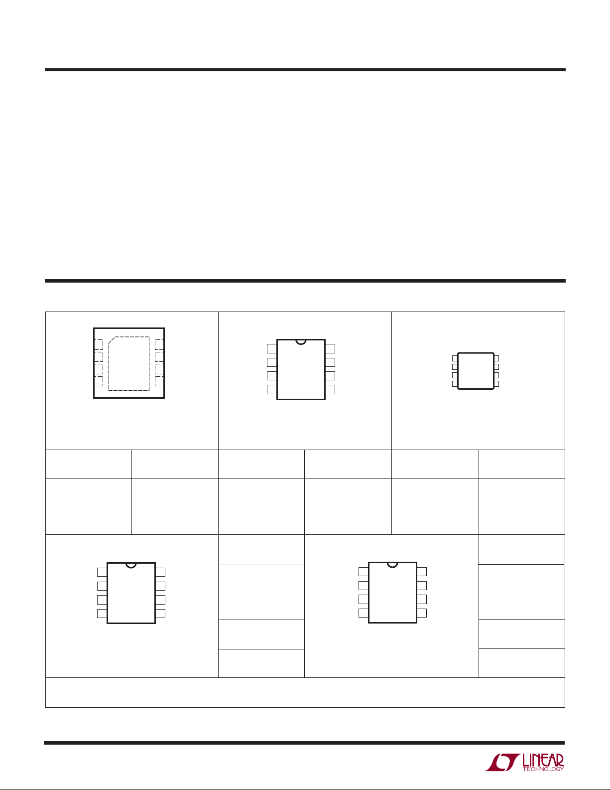
PACKAGE/ORDER INFORMATION
TOP VIEW
TOP VIEW
1NULL
–IN A
2
+IN A
3
–
V
4
8-LEAD (3mm × 3mm) PLASTIC DFN
UNDERSIDE METAL CONNECTED TO V
DD PACKAGE
T
= 125°C, θJA = 160°C/ W (DD)
JMAX
(PCB CONNECTION OPTIONAL)
ORDER PART
NUMBER
LTC1440CDD
LTC1440IDD
TOP VIEW
OUT A
1
–
V
2
+
IN A
3
–
IN A
4
N8 PACKAGE
8-LEAD PDIP
T
= 150°C, θJA = 130°C/ W (N8)
JMAX
= 150°C, θJA = 175°C/ W (S8)
T
JMAX
Order Options Tape and Reel: Add #TR
Lead Free: Add #PBF Lead Free Tape and Reel: Add #TRPBF Lead Free Part Marking: http://www.linear.com/leadfree/
8
NULL
+
V
7
OUT
6
SHDN
5
DD8 PART
MARKING*
LBTH
OUT B
8
+
V
7
IN B
6
IN B
5
S8 PACKAGE
8-LEAD PLASTIC SO
GND
1
–
V
2
+
IN
3
–
IN
4
N8 PACKAGE
8-LEAD PDIP
T
–
T
JMAX
JMAX
8-LEAD PLASTIC SO
= 150°C, θJA = 130°C/ W (N8)
= 150°C, θJA = 175°C/ W (S8)
ORDER PART
NUMBER
LTC1440CN8
LTC1440CS8
OUT
8
V
7
REF
6
HYST
5
S8 PACKAGE
S8 PART
MARKING
1440
1440I
+
GND
V
IN
IN
T
ORDER PART
NUMBER
LTC1440CMS8
LTC1440IMS8
LTC1440IN8
LTC1440IS8
ORDER PART
NUMBER
LTC1441CN8
LTC1441CS8
+
–
LTC1441IN8
LTC1441IS8
S8 PART
MARKING
OUT A
V
IN A
IN B
N8 PACKAGE
8-LEAD PDIP
1441
TOP VIEW
1
–
2
+
3
–
4
S8 PACKAGE
8-LEAD PLASTIC SO
T
= 150°C, θJA = 130°C/ W (N8)
JMAX
T
= 150°C, θJA = 175°C/ W (S8)
JMAX
OUT B
8
+
V
7
REF
6
HYST
5
1441I
TOP VIEW
1
–
2
+
3
–
4
MS8 PACKAGE
8-LEAD PLASTIC MSOP
= 150°C, θJA = 250°C/ W
JMAX
ORDER PART
LTC1442CN8
LTC1442CS8
LTC1442IN8
LTC1442IS8
OUT
8
+
7
V
6
REF
5
HYST
MS8 PART
MARKING*
LTBX
NUMBER
S8 PART
MARKING
1442
1442I
Consult LTC Marketing for parts specified with wider operating temperature ranges.
* The temperature grade is identified by a label on the shipping container.
2
144012fb
LTC1440/LTC1441/LTC1442
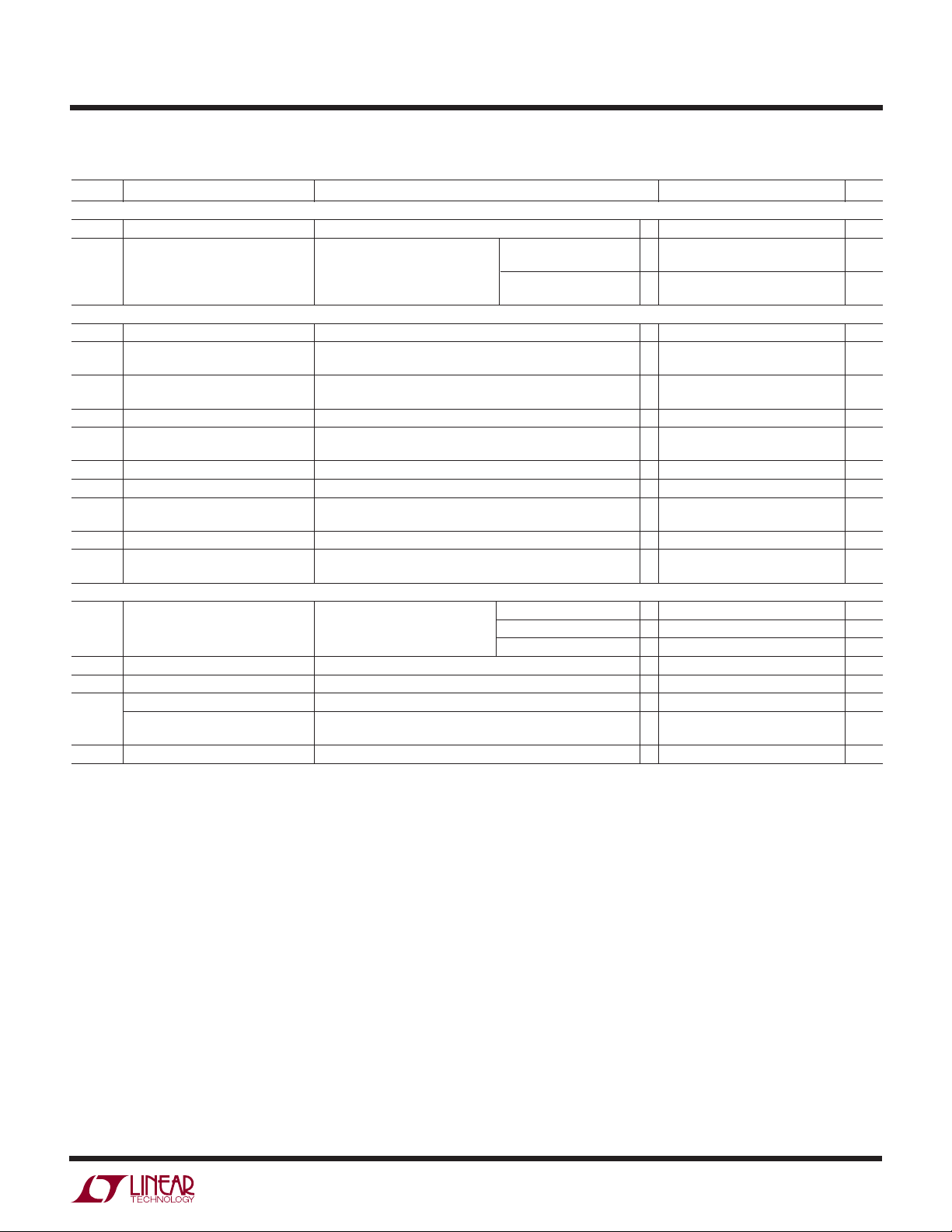
ELECTRICAL CHARACTERISTICS
temperature range, otherwise specifications are at T
The ● denotes the specifications which apply over the full operating
= 25°C. V+ = 5V and V– = GND = 0V unless otherwise noted.
A
SYMBOL PARAMETER CONDITIONS MIN TYP MAX UNITS
Power Supply
+
V
I
CC
Supply Voltage Range
Supply Current IN+ = IN– + 80mV LTC1440 CTemp Range
HYST = REF (LTC1440/LTC1442) I Temp Range
LTC1441
LTC1442
●
●
●
●
●
2.0 11.0 V
2.1 4.0 µA
4.4 µA
3.5 5.7 µA
3.5 5.7 µA
Comparator
V
OS
I
IN
V
CM
Comparator Input Offset Voltage VCM = 2.5V
Input Leakage Current (IN+, IN–)V
+
= V
IN
IN
Input Leakage Current (HYST)
Comparator Input Common
–
= 2.5V
●
●
●
●
V
±3 ±10 mV
±0.01 ±1.0 nA
±0.02 ±1.0 nA
–
V+ – 1.3V V
Mode Range
CMRR Common Mode Rejection Ratio V– to V+ – 1.3V 0.1 1 mV/V
+
PSRR Power Supply Rejection Ratio V
= 2V to 11V (LTC1441) 0.1 1 mV/V
V+ = 2.5V to 11V (LTC1440/LTC1442) 0.1 1 mV/V
NOISE Voltage Noise 100Hz to 100kHz 100 µV
V
t
PD
HYST
Hysteresis Input Voltage Range LTC1440/LTC1442
Propagation Delay C
= 100pF Overdrive = 10mV 15 µs
OUT
●
REF – 50mV REF V
RMS
Overdrive = 100mV 8 µs
V
OH
V
OL
Output High Voltage IO = – 13mA
Output Low Voltage IO = 1.8mA LTC1440
LTC1441/LTC1442
●
V+ – 0.4V V
●
●
GND + 0.4V V
V– + 0.4V V
Reference
V
REF
I
SOURCE
I
SINK
∆V
NOISE Voltage Noise 100Hz to 100kHz 100 µV
Reference Voltage No Load C Temp Range
LTC1440/LTC1442 I Temp Range
LTC1440 (MSOP, DFN)
Reference Output Source Current ∆V
Reference Output Sink Current ∆V
Reference Source Current 0 ≤ I
REF
Reference Sink Current 0 ≤ I
≤ 1mV (LTC1442)
REF
≤ 2.5mV (LTC1442) 10 20 µA
REF
≤ 2mA (LTC1440)
SOURCE
≤ 10µA (LTC1440) 0.5 1.5 mV
SINK
●
1.170 1.182 1.194 V
●
1.164 1.200 V
●
1.164 1.200 V
●
100 200 µA
●
●
0.8 5 mV
5mV
RMS
144012fb
3
LTC1440/LTC1441/LTC1442
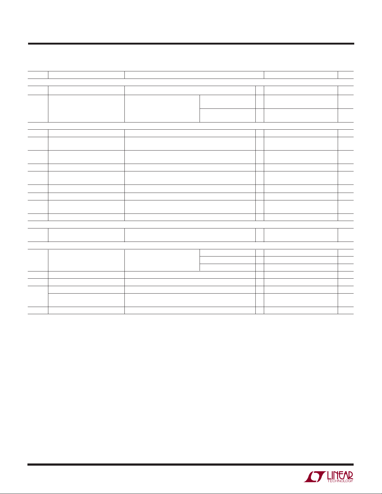
ELECTRICAL CHARACTERISTICS
temperature range, otherwise specifications are at T
The ● denotes the specifications which apply over the full operating
= 25°C. V+ = 3V and V– = GND = 0V unless otherwise noted.
A
SYMBOL PARAMETER CONDITIONS MIN TYP MAX UNITS
Power Supply
+
V
I
CC
Supply Voltage Range
Supply Current IN+ = IN– + 80mV LTC1440 CTemp Range
HYST = REF (LTC1440/LTC1442) I Temp Range
LTC1441
LTC1442
●
●
●
●
●
211V
2 3.9 µA
4.3 µA
3.5 5.7 µA
3.5 5.7 µA
Comparator
V
OS
I
IN
V
CM
Comparator Input Offset Voltage VCM = 1.5V
Input Leakage Current (IN+, IN–)V
+
= V
IN
IN
Input Leakage Current (HYST)
Comparator Input Common
–
= 1.5V
●
●
●
●
V
±3 ± 10 mV
±0.01 ±1nA
±0.02 ±1nA
–
V+ – 1.3V V
Mode Range
CMRR Common Mode Rejection Ratio V– to V+ – 1.3V 0.1 1 mV/V
+
PSRR Power Supply Rejection Ratio V
= 2V to 11V (LTC1441) 0.1 1 mV/V
V+ = 2.5V to 11V (LTC1440/LTC1442) 0.1 1 mV/V
NOISE Voltage Noise 100Hz to 100kHz 100 µV
V
t
PD
HYST
Hysteresis Input Voltage Range LTC1440/LTC1442
Propagation Delay C
= 100pF Overdrive = 10mV 14 µs
OUT
●
REF – 50mV REF V
RMS
Overdrive = 100mV 5 µs
V
OH
Output High Voltage IO = – 8mA
●
V+ – 0.4V V
Comparator
V
OL
Output Low Voltage IO = 0.8mA LTC1440
LTC1441/LTC1442
●
●
GND + 0.4V V
V– + 0.4V V
Reference
V
REF
I
SOURCE
I
SINK
∆V
NOISE Voltage Noise 100Hz to 100kHz 100 µV
Reference Voltage No Load C Temp Range
LTC1440/LTC1442 I Temp Range
LTC1440 (MSOP, DFN)
Reference Output Source Current ∆V
Reference Output Sink Current ∆V
Reference Source Current 0 ≤ I
REF
Reference Sink Current 0 ≤ I
≤ 1mV (LTC1442)
REF
≤ 2.5mV (LTC1442) 10 20 µA
REF
≤ 1mA (LTC1440)
SOURCE
≤ 10µA (LTC1440) 0.5 1.5 mV
SINK
●
1.170 1.182 1.194 V
●
1.164 1.200 V
●
1.164 1.200 V
●
●
●
60 120 µA
0.8 5.5 mV
5mV
RMS
Note 1: Absolute Maximum Ratings are those values beyond which the life
of a device may be impaired.
4
144012fb
LTC1440/LTC1441/LTC1442
UW
TYPICAL PERFOR A CE CHARACTERISTICS
Comparator Response Time vs
Input Overdrive
5
TA = 25°C
4
3
2
1
0
0
100
INPUT VOLTAGE (mV) OUTPUT VOLTAGE (V)
–1
100mV 10mV
50mV 20mV
20108
RESPONSE TIME (µs)
Comparator Short-Circuit Sink
Current vs Supply Voltage
200
TA = 25°C
180
160
140
120
100
80
60
SINK CURRENT (mA)
40
20
0
OUT CONNECTED TO V
213579
0
4
SUPPLY VOLTAGE (V)
Comparator Response Time vs
Input Overdrive
5
TA = 25°C
4
3
2
1
0
100
0
64
1440/1/2 G01
INPUT VOLTAGE (mV) OUTPUT VOLTAGE (V)
100mV
–1
08
50mV
20mV
10mV
16
12
210
4
6
RESPONSE TIME (µs)
14
1440/1/2 G02
18
Comparator Short-Circuit Source
Current vs Supply Voltage
160
140
+
6
8
10
1440/1/2 G03
120
100
80
60
SOURCE CURRENT (mA)
40
20
0
0
OUT CONNECTED TO
12 4
SUPPLY VOLTAGE (V)
–
= GND = 0V
V
3
5
1440/1/2 G04
144012fb
5

LTC1440/LTC1441/LTC1442
UW
TYPICAL PERFOR A CE CHARACTERISTICS
Comparator Response Time vs
Load Capacitance with 100mV
Input Overdrive
12
Comparator Response Time at
Low Supply Voltage
10000
10
8
6
RESPONSE TIME (µs)
4
2
0
t
PHL
t
PLH
20
LOAD CAPACITANCE (nF)
60
40
80
1440/1/2 G05
100
1000
RESPONSE TIME (µs)
100
20mV OVERDRIVE
10
1
1.0
100mV OVERDRIVE
1.2 1.4 1.61.1 1.3 1.5
SUPPLY VOLTAGE (V)
1440/1/2 G06
Comparator Output Voltage High
vs Load Current
5
4
3
V+ = 3V
2
OUTPUT VOLTAGE HIGH (V)
V+ = 2V
V+ = 5V
TA = 25°C
6
1
0
10 20 30 40
LOAD CURRENT (mA)
50 60
1440/1/2 G07
144012fb

LTC1440/LTC1441/LTC1442
UW
TYPICAL PERFOR A CE CHARACTERISTICS
Comparator Output Voltage Low
vs Load Current
2.5
TA = 25°C
2.0
V+ = 2V
1.5
1.0
OUTPUT VOLTAGE LOW (V)
0.5
0
0
10 20
V+ = 3V
40
30 50 80
LOAD CURRENT (mA)
V+ = 5V
60 70
1440/1/2 G08
LTC1440
Supply Current vs Temperature
6
5
4
V+ = 5V
–
= –5V
V
LTC1440/LTC1442
Hysteresis Control
80
60
40
20
0
–20
–40
–60
POSITIVE-TO-NEGATIVE INPUT VOLTAGE (mV)
–80
10 20 40
0
V
– V
REF
OUTPUT HIGH
OUTPUT LOW
30
(mV)
HYST
50
1440/1/2 G09
3
V+ = 3V
V+ = 5V
–
= GND = 0V
V
60
–
= GND = 0V
V
100
140
1440/1/2 G10
144012fb
SUPPLY CURRENT (µA)
2
1
–20–40
–60
20 40 80 1200
TEMPERATURE (°C)
7

LTC1440/LTC1441/LTC1442
UW
TYPICAL PERFOR A CE CHARACTERISTICS
Reference Output Voltage vs
Output Load Current
1.190
VCC = 5V
1.185
1.180
1.175
1.170
1.165
REFERENCE OUTPUT VOLTAGE (V)
1.160
1.155
0
0.5 1.0
1.5 2.5
OUTPUT LOAD CURRENT (mA)
SOURCE
2.0 3.0
1440/1/2 G11
3.5
Reference Voltage vs
Temperature
1.186
1.184
1.182
1.180
1.178
1.176
1.174
REFERENCE VOLTAGE (V)
1.172
1.170
–60
–20–40
TEMPERATURE (°C)
Reference Output Voltage vs
Output Load Current (Sink)
1.200
VCC = 2V
1.195
1.190
1.185
1.180
1.175
REFERENCE OUTPUT VOLTAGE (V)
1.170
0
5
OUTPUT LOAD CURRENT (µA)
60
100
20 40 80 1200
140
1440/1/2 G13
SINK
10 15 20
VCC = 5V
25 30
1440/1/2 G12
8
144012fb

UUU
PIN FUNCTIONS
1
GND
V
2
IN
3
IN
4
LTC1440
–
+
+
–
–
OUT
REF
HYST
LTC1440/LTC1441/LTC1442
OUT A
8
7
+
V
6
5
OUT A
2
–
V
IN A
3
IN A
4
LTC14411
A
+
–
+
–
OUT B
8
7
+
V
B
+
–
+
IN B
6
–
IN B
5
1
2
V
IN A
3
4
IN B
LTC1442
–
A
+
–
+
–
–
V
B
–
OUT B
+
REF
HYST
+
V
1440/1/2 PD
8
7
6
5
LTC1440
GND (Pin 1): Ground. Connect to V– for single supply
operation.
V– (Pin 2): Negative Supply. Connect to ground for single
supply operation. Potential should be more negative than
GND.
IN+ (Pin 3): Noninverting Comparator Input. Input common mode range from V– to V+ –1.3V. Input current
typically 10pA at 25°C.
IN– (Pin 4): Inverting Comparator Input. Input common
mode range from V– to V+ –1.3V. Input current typically
10pA at 25°C.
HYST (Pin 5): Hysteresis Input. Connect to REF if not
used. Input voltage range is from V
REF
to V
– 50mV.
REF
REF (Pin 6): Reference Output. 1.182V with respect
to V–. Can source up to 200µA and sink 15µA at 25°C.
Drive 0.01µF bypass capacitor without oscillation.
V+ (Pin 7): Positive Supply. 2V to 11V.
OUT (Pin 8): Comparator CMOS Output. Swings from
+
GND to V
. Output can source up to 40mA and sink 5mA.
LTC1441
IN B– (Pin 5): Inverting Input of Comparator B. Input
–
common mode range from V
to V+ –1.3V. Input current
typically 10pA at 25°C.
+
IN B
(Pin 6): Noninverting Input of Comparator B. Input
common mode range from V– to V+ –1.3V. Input current
typically 10pA at 25°C.
V+ (Pin 7): Positive Supply. 2V to 11V.
OUT B (Pin 8): Comparator B CMOS Output. Swings from
V– to V+. Output can source up to 40mA and sink 5mA.
LTC1442
OUT A (Pin 1): Comparator A CMOS Output. Swings from
V– to V+. Output can source up to 40mA and sink 5mA.
V– (Pin 2): Negative Supply.
IN A+ (Pin 3): Noninverting Input of Comparator A. Input
common mode range from V– to V+ –1.3V. Input current
typically 10pA at 25°C.
IN B– (Pin 4): Inverting Input of Comparator B. Input
common mode range from V– to V+ –1.3V. Input current
typically 10pA at 25°C.
HYST (Pin 5): Hysteresis Input. Connect to REF if not
used. Input voltage range is from V
REF
to V
– 50mV.
REF
OUT A (Pin 1): Comparator A CMOS Output. Swings from
V– to V+. Output can source up to 40mA and sink 5mA.
V– (Pin 2): Negative Supply.
IN A+ (Pin 3): Noninverting Input of Comparator A. Input
common mode range from V– to V+ –1.3V. Input current
typically 10pA at 25°C.
IN A– (Pin 4): Inverting Input of Comparator A. Input
common mode range from V– to V+ –1.3V. Input current
typically 10pA at 25°C.
REF (Pin 6): Reference Output. 1.182V with respect
to V–. Can source up to 200µA and sink 15µA at 25°C.
Drive 0.01µF bypass capacitor without oscillation.
V+ (Pin 7): Positive Supply. 2V to 11V.
OUT B (Pin 8): Comparator B CMOS Output. Swings from
–
to V+. Output can source up to 40mA and sink 5mA.
V
144012fb
9

LTC1440/LTC1441/LTC1442
U
WUU
APPLICATIONS INFORMATION
LTC1440/LTC1441/LTC1442 are a family of micropower
comparators with built-in 1.182V reference. Features
include programmable hysteresis (LTC1440/LTC1442),
wide supply voltage range (2V to 11V) and the ability of the
reference to drive up to a 0.01µF capacitor without oscil-
lation. The comparators’ CMOS outputs can source up to
40mA and the supply current glitches, that normally occur
when switching logic states, have been eliminated.
Power Supplies
The comparator family operates from a single 2V to 11V
supply. The LTC1440 includes a separate ground for the
comparator output stage, allowing a split supply ranging
from ± 1V to ± 5.5V. Connecting V
will allow single supply operation. If the comparator output is required to source more than 1mA, or the supply
source impedance is high, V+ should be bypassed with a
0.1µF capacitor.
–
to GND on the LTC1440
capacitor of up to 0.01µF without oscillation and by
inserting a series resistor, capacitance values up to 100µF
can be used (Figure 1).
Figure 2 shows the resistor value required for different
capacitor values to achieve critical damping. Bypassing
the reference can help prevent false tripping of the comparators by preventing glitches on V
+
or reference load
transients from disturbing the reference output voltage.
Figure 3 shows the bypassed reference output with a
square wave applied to the V+ pin. Resistors R2 and R3 set
10mV of hysteresis voltage band while R1 damps the
reference response. Note that the comparator output
doesn’t trip.
REFERENCE
OUTPUT
REF
R1
LTC144X
Comparator Inputs
The comparator inputs can swing from the negative supply V– to within 1.3V max of the positive supply V+. The
–
inputs can be forced 300mV below V
or above V+ without
damage and the typical input leakage current is only
± 10pA.
Comparator Outputs
The LTC1440 comparator output swings between GND
+
and V
LTC1441 and LTC1442 outputs swing between V
to assure TTL compatibility with a split supply. The
–
and V+.
The outputs are capable of sourcing up to 40mA and
sinking up to 5mA while still maintaining microampere
quiescent currents. The output stage does not generate
crowbar switching currents during transitions which helps
minimize parasitic feedback through the supply pins.
Voltage Reference
The internal bandgap reference has a voltage of 1.182V
referenced to V
–
. The reference accuracy is 1.5% from
–40°C to 85°C. It can source up to 200µA and sink up to
20µA with a 5V supply. The reference can drive a bypass
C1
Figure 1. Damping the Reference Output
1000
100
10
RESISTOR VALUE (kΩ)
1
0.1
0.001
Figure 2. Damping Resistance vs Bypass Capacitor Value
0.01 0.1 101
CAPACITOR VALUE (µF)
V
–
1440/1/2 F01
1440/1/2 F02
10
144012fb

LTC1440/LTC1441/LTC1442
U
WUU
APPLICATIONS INFORMATION
7
+
+
IN
3
–
IN
4
5V
TO
8V
R2
10k
R3
2.4M
R1
430Ω
C1
1µ F
HYST
5
REF
6
Figure 3a. Reference Transient Response Test Circuit
8V
+
V
5V
V
REF
2mV/DIV
V
+
8
–
LTC1440
–
V
21
GND
1440/1/2 F03a
OUT
up to 15%. If hysteresis is not wanted, the HYST pin
should be shorted to REF. Acceptable values for I
REF
range
from 0.1µA to 5µA. If 2.4M is chosen for R2, then the value
of R1 is equal to the value of V
6
I
REF
R1
R2
Figure 4. Programmable Hysteresis
REF
LTC1440
5
HYST
V
.
HB
V
HB
R1 =
(2)(I
)
REF
V
I
REF
1440/1/2 F04
HB
)
2
1.182V –
(
–
2
R2 =
Level Detector
The LTC1440 is ideal for use as a micropower level
detector as shown in Figure 5. R1 and R2 form a voltage
divider from VIN to the noninverting comparator input. R3
and R4 set the hysteresis voltage, and R5 and C1 bypass
the reference output. The following design procedure can
be used to select the component values:
OUT
2ms/DIV 1440/1/2 F03b
Figure 3b. Reference and Comparator Output
Transient Response
Hysteresis
Hysteresis can be added to the LTC1440 by connecting a
resistor (R1) between the REF and HYST pins and a
second resistor (R2) from HYST to V– (Figure 4).
The difference between the upper and lower threshold
voltages, or hysteresis voltage band (V
), is equal to twice
HB
the voltage difference between the REF and HYST pins.
When more hysteresis is added, the upper threshold
increases the same amount as the low threshold decreases. The maximum voltage allowed between REF and
HYST pins is 50mV, producing a maximum hysteresis
voltage band of 100mV. The hysteresis band could vary by
1. Choose the V
V
IN
R2
3.4M
1%
R1
1.18M
1%
voltage trip level, in this example 4.65V.
IN
5V
7
+
V
+
–
LTC1440
–
V
21
GND
R3
15k
1%
R4
2.4M
1%
R5
430Ω
5%
C1
1µ F
+
IN
3
–
4
IN
5
HYST
6
REF
Figure 5. Glitch-Free Level Detector with Hysteresis
8
OUT
1440/1/2 F05
144012fb
11

LTC1440/LTC1441/LTC1442
U
WUU
APPLICATIONS INFORMATION
2. Calculate the required resistive divider ratio.
Ratio = V
Ratio = 1.182V/4.65V = 0.254
3. Choose the required hysteresis voltage band at the
input V
esis voltage band referred to the comparator input V
V
HB
V
HB
V
HB
4. Choose the values for R3 and R4 to set the hysteresis.
R4 = 2.4M
R3(kΩ) = VHB = 15k
5. Choose the values for R1 and R2 to set the trip point.
R
1
RR
21
REF/VIN
, in this example 60mV. Calculate the hyster-
HBIN
= (V
= (60mV)(0.254)
= 15.24mV
V
== =
I
BIAS
=
REF
⎡
⎢
⎢
⎢
⎢
⎣
HBIN
V
REF
)(Ratio)
.
1 182
µ
A
1
V
IN
V
HB
+
2
V
.
118
⎤
⎥
⎥
1
−
⎥
⎥
⎦
M
HB
.
⎡
⎢
⎢
.
2118
=
RM
⎢
⎢
⎣
.
=
RM
2340
Low Voltage Operation
The guaranteed minimum operating voltage is 2V or
(±1V). As the total supply voltage is reduced below 2V, the
performance degrades and the supply current falls. Both
the reference and the comparator are still functioning with
supply voltage down to 1.5V. The reference will have
slightly worse temperature coefficient. While the comparator would have less output drive and the propagation
delay increases. The useful input voltage range extends
from the negative supply to a little under 1V below the
positive supply, which is slightly closer to the positive rail
than the device operating from higher supply voltages.
.
1 182
.
465
+
V
V
15
mV
2
⎤
⎥
⎥
1
−
⎥
⎥
⎦
12
144012fb

U
TYPICAL APPLICATIONS
LTC1440/LTC1441/LTC1442
10-Bit 30µA A/D Converter
5V
LT®1034
1.2V
2N3809
150k
*TRW-IRC MRT–5/+120ppm/°C
100k
365k*
0.033µF
POLYSTYRENE
E
IN
0V TO 3V
10M
+
1/2 LTC1441
–
1N914
74C00
1M
5V
470k
32.768kHz
+
C2
1/2 LTC1441
–
1.2M
10pF
C1
VN2222LL
74C00
CONV
COMMAND
Q
D CLK
74C74
Q
74C00 74C00
STATUS
DATA
OUT
1440/1/2 TA03
Low Battery Detect Operates Down to 1.5V
+
–
GND
7
+
V
LTC1440
+
V
1
2-CELL
NiCd
2.6M
1M
20k
1.3M
1M
+
IN
3
–
4
IN
6
REF
5
HYST
32.768kHz “Watch Crystal” Oscillator
+
1/2
LTC1441
32.768kHz
OUT
1M
+V
470k
8
OUT
–
1.2M
10pF
–
V
2
1440 TA06
1440/1/2 TA05
144012fb
13

LTC1440/LTC1441/LTC1442
U
PACKAGE DESCRIPTIO
8-Lead Plastic DFN (3mm × 3mm)
(Reference LTC DWG # 05-08-1698)
0.675 ±0.05
DD Package
R = 0.115
TYP
0.38 ± 0.10
85
3.5 ±0.05
1.65 ±0.05
(2 SIDES)2.15 ±0.05
PACKAGE
OUTLINE
0.25 ± 0.05
RECOMMENDED SOLDER PAD PITCH AND DIMENSIONS
0.42 ± 0.038
(.0165 ± .0015)
0.50
BSC
2.38 ±0.05
(2 SIDES)
5.23
(.206)
MIN
TYP
RECOMMENDED SOLDER PAD LAYOUT
DETAIL “A”
0.254
(.010)
GAUGE PLANE
DETAIL “A”
0.18
(.007)
NOTE:
1. DIMENSIONS IN MILLIMETER/(INCH)
2. DRAWING NOT TO SCALE
3. DIMENSION DOES NOT INCLUDE MOLD FLASH, PROTRUSIONS OR GATE BURRS.
MOLD FLASH, PROTRUSIONS OR GATE BURRS SHALL NOT EXCEED 0.152mm (.006") PER SIDE
4. DIMENSION DOES NOT INCLUDE INTERLEAD FLASH OR PROTRUSIONS.
INTERLEAD FLASH OR PROTRUSIONS SHALL NOT EXCEED 0.152mm (.006") PER SIDE
5. LEAD COPLANARITY (BOTTOM OF LEADS AFTER FORMING) SHALL BE 0.102mm (.004") MAX
PIN 1
TOP MARK
(NOTE 6)
0.200 REF
NOTE:
1. DRAWING TO BE MADE A JEDEC PACKAGE OUTLINE M0-229 VARIATION OF (WEED-1)
2. DRAWING NOT TO SCALE
3. ALL DIMENSIONS ARE IN MILLIMETERS
4. DIMENSIONS OF EXPOSED PAD ON BOTTOM OF PACKAGE DO NOT INCLUDE
MOLD FLASH. MOLD FLASH, IF PRESENT, SHALL NOT EXCEED 0.15mm ON ANY SIDE
5. EXPOSED PAD SHALL BE SOLDER PLATED
6. SHADED AREA IS ONLY A REFERENCE FOR PIN 1 LOCATION
ON TOP AND BOTTOM OF PACKAGE
MS8 Package
8-Lead Plastic MSOP
(Reference LTC DWG # 05-08-1660)
0.889
± 0.127
(.035 ± .005)
3.20 – 3.45
(.126 – .136)
3.00 ± 0.102
PLANE
(.118 ± .004)
(NOTE 3)
4.90
± 0.152
(.193 ± .006)
0.22 – 0.38
(.009 – .015)
TYP
1.10
(.043)
MAX
0.65
(.0256)
BSC
0.65
(.0256)
BSC
° – 6° TYP
0
0.53 ± 0.152
(.021 ± .006)
SEATING
3.00 ±0.10
(4 SIDES)
0.75 ±0.05
8
7
12
0.00 – 0.05
6
5
4
3
1.65 ± 0.10
(2 SIDES)
0.25 ± 0.05
BOTTOM VIEW—EXPOSED PAD
0.52
(.0205)
REF
3.00 ± 0.102
(.118 ± .004)
(NOTE 4)
0.86
(.034)
REF
0.127 ± 0.076
(.005 ± .003)
MSOP (MS8) 0204
2.38 ±0.10
(2 SIDES)
14
0.50 BSC
(DD8) DFN 1203
144012fb
14

PACKAGE DESCRIPTION
U
LTC1440/LTC1441/LTC1442
N8 Package
8-Lead PDIP (Narrow 0.300)
(LTC DWG # 05-08-1510)
.400*
(10.160)
MAX
87 6
.255 ± .015*
(6.477 ± 0.381)
5
12
.300 – .325
(7.620 – 8.255)
.065
(1.651)
.008 – .015
(0.203 – 0.381)
+.035
.325
–.015
+0.889
8.255
()
–0.381
NOTE:
1. DIMENSIONS ARE
*THESE DIMENSIONS DO NOT INCLUDE MOLD FLASH OR PROTRUSIONS.
MOLD FLASH OR PROTRUSIONS SHALL NOT EXCEED .010 INCH (0.254mm)
INCHES
MILLIMETERS
TYP
.045 – .065
(1.143 – 1.651)
.100
(2.54)
BSC
S8 Package
8-Lead Plastic Small Outline (Narrow 0.150)
(LTC DWG # 05-08-1610)
.050 BSC
.045 ±.005
(4.801 – 5.004)
8
3
.189 – .197
NOTE 3
7
4
.130 ± .005
(3.302 ± 0.127)
.120
(3.048)
MIN
.018 ± .003
(0.457 ± 0.076)
5
6
.020
(0.508)
MIN
N8 1002
.245
MIN
.030 ±.005
TYP
RECOMMENDED SOLDER PAD LAYOUT
.010 – .020
(0.254 – 0.508)
.008 – .010
(0.203 – 0.254)
NOTE:
1. DIMENSIONS IN
2. DRAWING NOT TO SCALE
3. THESE DIMENSIONS DO NOT INCLUDE MOLD FLASH OR PROTRUSIONS.
MOLD FLASH OR PROTRUSIONS SHALL NOT EXCEED .006" (0.15mm)
Information furnished by Linear Technology Corporation is believed to be accurate and reliable.
However, no responsibility is assumed for its use. Linear Technology Corporation makes no representation that the interconnection of its circuits as described herein will not infringe on existing patent rights.
× 45°
.016 – .050
(0.406 – 1.270)
INCHES
(MILLIMETERS)
.160
±.005
0°– 8° TYP
.228 – .244
(5.791 – 6.197)
.053 – .069
(1.346 – 1.752)
.014 – .019
(0.355 – 0.483)
TYP
1
2
.150 – .157
(3.810 – 3.988)
NOTE 3
3
4
.004 – .010
(0.101 – 0.254)
.050
(1.270)
BSC
SO8 0303
144012fb
15

LTC1440/LTC1441/LTC1442
U
TYPICAL APPLICATION
10kHz TRIM
INPUT
0V TO 5V
1.2M*
= HP5082-2810
= 1N4148
= 2N2222
= 1% METAL FILM
*
= POLYSTYRENE
**
200k
0.01µF
–
C1
1/2 LTC1441
+
100k
Q5
Q6
Q7
10kHz V/F Converter
+
2.2µF
50pF
2M TYP
100Hz TRIM
15k
100pF**
10M
C2
1/2 LTC1441
+V
6.2V TO 12V
LM334
2k*
Q1
LT1034-1.2
LT1034-1.2
Q2
Q3
Q4
2.7M
0.1µF
Q8
74C14
+
0.47µF
f
OUT
0kHz TO 10kHz
–
+
1440/1/2 TA04
RELATED PARTS
PART NUMBER DESCRIPTION COMMENTS
LTC1443 1.182V Reference with Micropower Quad Comparators 1% Accuracy, 8.5µA Maximum Current, Ref Output Drives 0.01µF
LTC1444/LTC1445 1.2V Reference with Quad Comparator 1% Accuracy, 8.5µA Maximum Current, Ref Output Drives 0.01µF
with Adjustable Hysteresis
LTC1540 1.182V Reference with Nanopower Comparator DFN Package 0.3µA Quiescent Current (Typical), Reference
with Adjustable Hysteresis Drives 0.01µF
LTC1541 1.2V Reference with Micropower Amplifier and Comparator DFN Package 1.25% Accuracy, Rail-to-Rail Out, Low Offset Amplifier
LTC1842/LTC1843 1.82V Reference with Dual Comparators 1% Accuracy, Open-Drain Out, Reference Drives 0.01µF
with Adjustable Hysteresis
LTC1998 1.2 Reference with Comparator with Adjustable Thesholds Li-Ion Low Battery Monitor, SOT23, 1% Accuracy
LT6700-1 0.4 Reference with Low Voltage Dual Comparators SOT23, 1.4V to 18.5V Supply Range, ±2% Over Temperature
LT6700-2/LT6700-3
C-Load is a trademark of Linear Technology Corporation.
144012fb
LT/LWI/LT 0605 REV B • PRINTED IN USA
© LINEAR TECHNOLOGY CORPORATION 1996
16
Linear Technology Corporation
1630 McCarthy Blvd., Milpitas, CA 95035-7417
(408) 432-1900 ● FAX: (408) 434-0507
●
www.linear.com
 Loading...