

Linear Technology LTC1430A Datasheet
LTC1430A
High Power Step-Down
Switching Regulator Controller
EATU
F
■
High Power 5V to 1.xV-3.xV Switching Controller:
RE
S
Can Exceed 10A Output
■
Maximum Duty Cycle > 90% Permits 3.3V to 2.xV
Conversion Using a Low Power 5V Supply
■
All N-Channel External MOSFETs
■
Fixed Frequency Operation—Small L
■
Excellent Output Regulation: ±1% Over Line, Load
and Temperature Variations
■
High Efficiency: Over 95% Possible
■
No Low Value Sense Resistor Needed
■
Outputs Can Drive External FETs with Up to
10,000pF Gate Capacitance
■
Quiescent Current: 350µA Typ, 1µA in Shutdown
■
Fast Transient Response
■
Adjustable or Fixed 3.3V Output
■
Available in 8-Lead SO and 16-Lead GN
and SO Packages
U
O
PPLICATI
A
■
Power Supply for Pentium® II and AMD-K6
S
®
Microprocessors
■
High Power 5V to 3.xV Regulators
■
Local Regulation for Dual Voltage Logic Boards
■
Low Voltage, High Current Battery Regulation
DUESCRIPTIO
The LTC®1430A is a high power, high efficiency switching
regulator controller optimized for 5V to 1.xV-3.xV applications. It includes a precision internal reference and an
internal feedback system that can provide output regulation of ±1% over temperature, load current and line voltage
shifts. The LTC1430A uses a synchronous switching architecture with two N-channel output devices, eliminating the
need for a high power, high cost P-channel device. Additionally, it senses output current across the drain-source
resistance of the upper N-channel FET, providing an
adjustable current limit without an external low value sense
resistor.
The LTC1430A includes a fixed frequency PWM oscillator
for low output ripple under virtually all operating conditions. The 200kHz free-running clock frequency can be
externally adjusted from 100kHz to above 500kHz. The
LTC1430A’s maximum duty cycle is typically 93.5% compared to 88% for the LTC1430. This permits 3.3V to 2.xV
conversion using a low power 5V supply. The LTC1430A
features low 350µA quiescent current, allowing greater
than 90% efficiency operation in converter designs from
1A to greater than 50A output current. Shutdown mode
drops the LTC1430A supply current to 1µA.
, LTC and LT are registered trademarks of Linear Technology Corporation.
Pentium is a registered trademark of Intel Corporation.
AMD-K6 is a registered trademark of Advanced Micro Devices, Inc.
4.7µF
U
O
A
PPLICATITYPICAL
TA = 25°C
= 5V
PV
CC
V
= 3.3V
OUT
Efficiency
LOAD CURRENT (A)
10
1430 TA02
Typical 5V to 3.3V, 10A Application
5V
+
C
IN
220µF
×4
Q1A, Q1B
2 IN PARALLEL
2.7µH/15A
+
Q2
C
OUT
330µF
×6
1430 TA01
3.3V
10A
CC2
LTC1430A
SENSE
SENSE
PV
PGND
–
CC1
I
MAX
GND
MBR0530T1
G1
I
FB
G2NC
+
FB NC
16k
0.1µF
1k
Q1A, Q1B, Q2: MOTOROLA MTD20N03HL
: AVX-TPSE227M010R0100
C
IN
: AVX-TPSE337M006R0100
C
OUT
0.1µF
+
0.1µF
SHUTDOWN
R
7.5k
0.01µF
C
C
C
4700pF
1µF
PV
V
CC
SS
FREQSET
SHDN
COMP
100Ω
+
C1
220pF
100
90
80
70
EFFICIENCY (%)
60
50
40
0.1 1
1
LTC1430A
A
W
O
LUTEXI TIS
S
A
WUW
U
ARB
G
Supply Voltage
VCC....................................................................... 9V
PV
.............................................................. 13V
CC1, 2
Input Voltage
IFB......................................................... –0.3V to 18V
All Other Inputs ...................... –0.3V to (VCC + 0.3V)
WU
/
PACKAGE
G1
PV
CC1
GND
FB
T
JMAX
O
RDER I FOR ATIO
TOP VIEW
1
2
3
4
S8 PACKAGE
8-LEAD PLASTIC SO
= 150°C, θJA = 150°C/W
ORDER
PART NUMBER
G2
8
/PV
V
7
CC
CC2
COMP
6
SHDN
5
LTC1430ACS8
S8 PART MARKING
1430A
(Note 1)
Junction Temperature........................................... 150°C
Operating Temperature Range
LTC1430AC ............................................. 0°C to 70°C
LTC1430AI ........................................ – 40°C to 85°C
Storage Temperature Range ................ –65°C to 150°C
Lead Temperature (Soldering, 10 sec)................. 300°C
U
TOP VIEW
1
G1
2
PV
CC1
3
PGND
4
GND
–
SENSE
SENSE
16-LEAD PLASTIC SSOP
5
6
FB
+
7
8
SHDN
GN PACKAGE
T
= 150°C, θJA = 130°C/W (GN)
JMAX
T
= 150°C, θJA = 110°C/W (S)
JMAX
G2
16
PV
15
CC2
V
14
CC
I
13
FB
I
12
MAX
FREQSET
11
COMP
10
SS
9
S PACKAGE
16-LEAD PLASTIC SO
ORDER
PART NUMBER
LTC1430ACGN
LTC1430AIGN
LTC1430ACS
Consult factory for Military grade parts.
ELECTRICAL CHARACTERISTICS
VCC = 5V, T
SYMBOL PARAMETER CONDITIONS MIN TYP MAX MIN TYP MAX UNITS
V
CC
PV
CC
V
OUT
V
FB
∆V
OUT
I
VCC
I
PVCC
f
OSC
= 25°C (Note 2) unless otherwise noted.
A
LTC1430AC LTC1430AI
Supply Voltage ● 4848V
PV
, PV
CC1
Output Voltage Figure 1 3.30 3.30 V
Feedback Voltage SENSE+ and SENSE– Floating , ● 1.25 1.265 1.28 1.23 1.265 1.29 V
Output Load Regulation Figure 1, I
Output Line Regulation Figure 1, V
Supply Current (VCC Only) Figure 2, V
Supply Current (PVCC) Figure 2, PVCC = 5V, V
Internal Oscillator Frequency FREQSET Floating ● 140 200 260 130 200 300 kHz
Voltage ● 313313V
CC2
= 2.5V
V
COMP
= 0A to 10A 5 5 mV
OUT
= 4.75V to 5.25V 1 1 mV
CC
= V
SHDN
V
= 0V 1 10 1 10 µA
SHDN
V
= 0V 0.1 0.1 µA
SHDN
CC
= VCC (Note 3) 1.5 1.5 mA
SHDN
● 350 700 350 700 µA
2
LTC1430A
ELECTRICAL CHARACTERISTICS
VCC = 5V, T
SYMBOL PARAMETER CONDITIONS MIN TYP MAX MIN TYP MAX UNITS
V
IH
V
IL
I
IN
g
mV
g
mI
A
V
I
MAX
I
SS
tr, t
s
t
NOV
DC
MAX
= 25°C (Note 2) unless otherwise noted.
A
LTC1430AC LTC1430AI
SHDN Input High Voltage ● 2.4 2.4 V
SHDN Input Low Voltage ● 0.8 0.8 V
SHDN Input Current ● ±0.1 ±1 ±0.1 ±1 µA
Error Amplifier Transconductance ● 350 650 1100 300 650 1200 µmho
I
Amplifier Transconductance (Note 4) 2400 2400 µmho
LIM
Error Amplifier Open-Loop Gain (Note 5) ● 40 48 40 48 dB
I
Sink Current V
MAX
I(MAX)
= V
CC
● 8 12 16 8 12 17 µA
Soft Start Source Current VSS = 0V ● –8 –12 –16 –8 –12 –17 µA
Driver Rise/Fall Time Figure 3, PV
Driver Non-Overlap Time Figure 3, PV
Maximum Duty Cycle Figure 3, V
= 1.265V
V
FB
= PV
CC1
CC1
COMP
= 5V 80 250 80 250 ns
CC2
= PV
= 5V 25 130 250 25 130 250 ns
CC2
= VCC, ● 90 93.5 89 93.5 %
The ● denotes specifications which apply over the full operating
temperature range.
Note 1: Absolute Maximum Ratings are those values beyond which the life
of a device may be impaired.
Note 2: All currents into device pins are positive; all currents out of device
pins are negative. All voltages are referenced to ground unless otherwise
specified.
Note 3: Supply current in normal operation is dominated by the current
needed to charge and discharge the external FET gates. This will vary with
the LTC1430A operating frequency, operating voltage and the external
FETs used.
Note 4: The I
normal (not current limited) operation, the I
Note 5: The open-loop DC gain and transconductance from the FB pin
(SENSE
amplifier can sink but cannot source current. Under
LIM
+
and SENSE– floating) to COMP pin will be AV and gm
output current will be zero.
LIM
V
respectively.
3
LTC1430A
TEMPERATURE (°C)
–40
70
DUTY CYCLE (%)
75
85
90
95
0
40
60
1430 G03
80
–20 20
80
100
100
V
COMP
= V
CC
VFB = 1.265V
LOAD CURRENT (A)
0
–1.0
∆V
OUT
(mV)
–0.8
–0.4
–0.2
0
0.4
1
5
7
1460 G06
–0.6
0.2
4
9
10
2
3
68
TA = 25°C
V
OUT
= 3.3V
V
CC
= 5V
FIGURE 4
UW
TYPICAL PERFOR A CE CHARACTERISTICS
I
Pin Sink Current
MAX
vs Temperature
14.0
VCC = 5V
13.5
Oscillator Frequency
vs Temperature
240
VCC = 5V
FREQSET FLOATING
230
Maximum Duty Cycle
vs Temperature
13.0
12.5
12.0
CURRENT (µA)
MAX
I
11.5
11.0
10.5
–40
–20 0
TEMPERATURE (°C)
40 80 100
20 60
Error Amplifier Transconductance
vs Temperature
850
800
750
700
650
600
550
500
450
TRANSCONDUCTANCE (µmho)
400
350
gm =
–20 20
–40
∆I
COMP
∆V
FB
0
TEMPERATURE (°C)
40
60 100
1430 G01
80
1430 G04
220
210
200
190
OSCILLATOR FREQUENCY (kHz)
180
170
(mV)
FB
∆V
–10
–40
–20 0
∆V
vs Temperature
FB
10
VCC = 5V
8
6
4
2
0
–2
–4
–6
–8
–20 0 40
–40
20 60
TEMPERATURE (°C)
20
TEMPERATURE (°C)
40 80 100
1430 G02
Load Regulation
60 80 100
1430 G05
4
OUTPUT VOLTAGE (V)
Output Voltage vs Load Current
with Current Limit
4.0
3.5
3.0
2.5
2.0
1.5
1.0
0.5
R
= 10k R
I(MAX)
TA = 25°C
= 5V
V
CC
FIGURE 4
0
24 8
0
LOAD CURRENT (A)
= 16k
I(MAX)
6
Supply Current
vs Oscillator Frequency
1000
TA = 25°C
= 5V
V
CC
FIGURE 4
100
10
SUPPLY CURRENT (mA)
1
12
10
1430 G07
0.1
0 200 300 400
100
OSCILLATOR FREQUENCY (kHz)
IV
CC
IPVCC (LOADED
WITH 10,000pF,
= 12V)
PV
CC
(NO LOAD,
IPV
CC
= 12V)
PV
CC
IPVCC (NO LOAD,
= 5V)
PV
CC
500
1430 G08

UU U
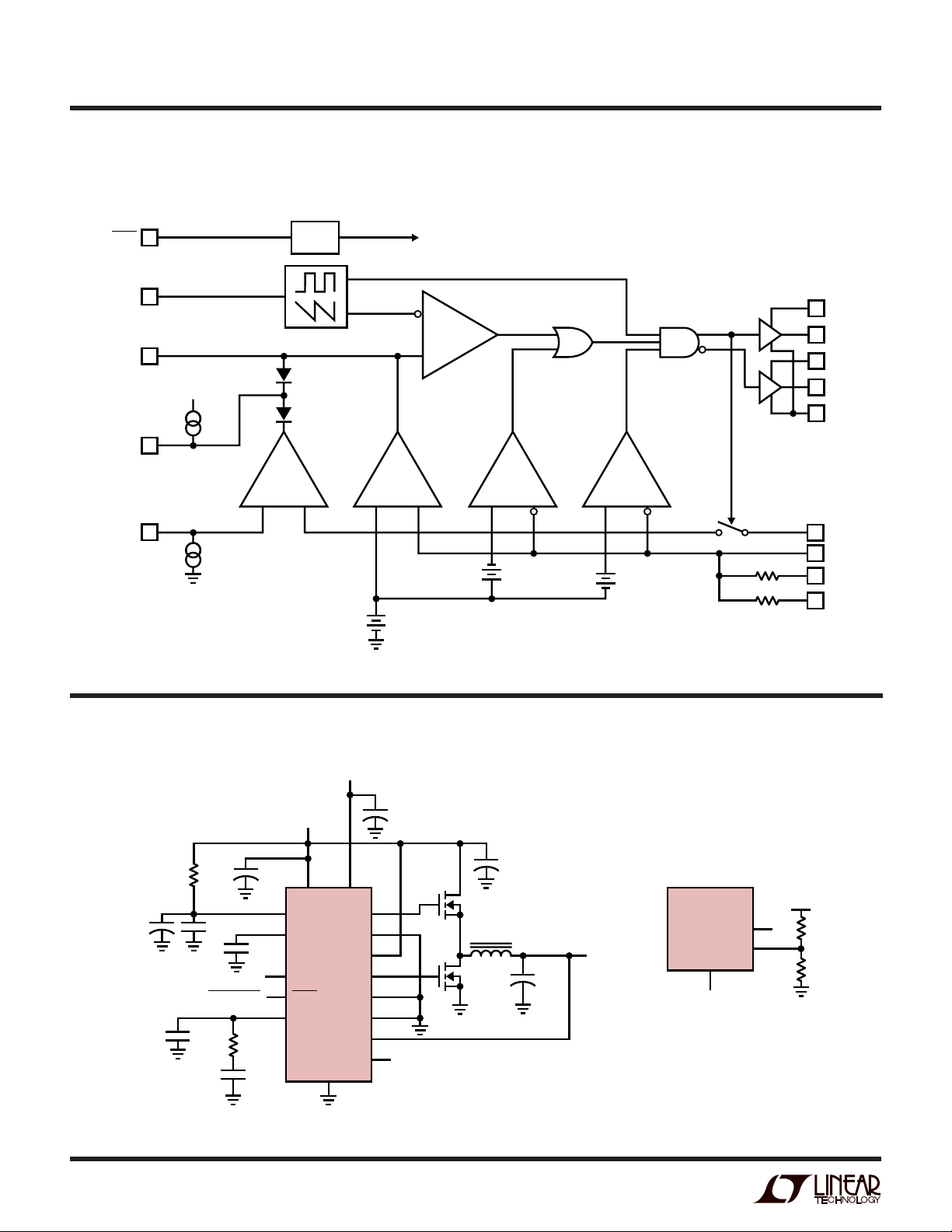
PI FU CTIO S
LTC1430A
(16-Lead Package/8-Lead Package)
G1 (Pin 1/Pin 1): Driver Output 1. Connect this pin to the
gate of the upper N-channel MOSFET, Q1. This output will
swing from PV
to PGND. It will always be low when G2
CC1
is high.
PV
(Pin 2/Pin 2): Power VCC for Driver 1. This is the
CC1
power supply input for G1. G1 will swing from PGND to
PV
. PV
CC1
PVCC + V
must be connected to a potential of at least
CC1
(Q1). This potential can be generated using
GS(ON)
an external supply or a simple charge pump connected to
the switching node between the upper MOSFET and the
lower MOSFET; see Applications Information for details.
PGND (Pin 3/Pin 3): Power Ground. Both drivers return to
this pin. It should be connected to a low impedance ground
in close proximity to the source of Q2. 8-lead parts have
PGND and GND tied together at Pin 3.
GND (Pin 4/Pin 3): Signal Ground. All low power internal
circuitry returns to this pin. To minimize regulation errors
due to ground currents, GND should be connected to
PGND right at the LTC1430A. 8-lead parts have PGND and
GND tied together internally at Pin 3.
SENSE–, FB, SENSE+ (Pins 5, 6, 7/Pin 4): These three
pins connect to the internal resistor divider and to the
internal feedback node. To use the internal divider to set
the output voltage to 3.3V, connect SENSE+ to the positive
terminal of the output capacitor and SENSE– to GND. FB
should be left floating in applications that use the internal
divider. To use an external resistor divider to set the output
voltage, float SENSE+ and SENSE– and connect the external resistor divider to FB.
COMP (Pin 10/Pin 6): External Compensation. The COMP
pin is connected directly to the output of the error amplifier
and the input of the PWM. An RC network is used at this
node to compensate the feedback loop to provide optimum transient response. See Applications Information for
compensation details.
FREQSET (Pin 11/NA): Frequency Set. This pin is used to
set the free running frequency of the internal oscillator.
With the pin floating, the oscillator runs at about 200kHz.
A resistor from FREQSET to ground will speed up the
oscillator; a resistor to VCC will slow it down. See Applications Information for resistor selection details.
I
(Pin 12/NA): Current Limit Set. I
MAX
sets the thresh-
MAX
old for the internal current limit comparator. If IFB drops
below I
limit. I
with G1 on, the LTC1430A will go into current
MAX
has a 12µA pull-down to GND. It can be adjusted
MAX
with an external resistor to PVCC or an external voltage
source.
IFB (Pin 13/NA): Current Limit Sense. Connect to the
switched node at the source of Q1 and the drain of Q2
through a 1k resistor. The 1k resistor is required to prevent
voltage transients from damaging IFB. This pin can be
taken up to 18V above GND without damage.
VCC (Pin 14/Pin 7): Power Supply. All low power internal
circuits draw their supply from this pin. Connect to a clean
power supply, separate from the main PVCC supply at the
drain of Q1. This pin requires a 4.7µF or greater bypass
capacitor. 8-lead parts have VCC and PV
tied together
CC2
at Pin 7 and require at least a 10µF bypass to GND.
SHDN (Pin 8/Pin 5): Shutdown. A TTL compatible low
level at SHDN for longer than 50µs puts the LTC1430A into
shutdown mode. In shutdown, G1 and G2 go low, all
internal circuits are disabled and the quiescent current
drops to 10µA max. A TTL compatible high level at SHDN
allows the part to operate normally.
SS (Pin 9/NA): Soft Start. The SS pin allows an external
capacitor to be connected to implement a soft start function. An external capacitor from SS to ground controls the
start-up time and also compensates the current limit loop,
allowing the LTC1430A to enter and exit current limit
cleanly. See Applications Information for more details.
PV
(Pin 15/Pin 7): Power VCC for Driver 2. This is the
CC2
power supply input for G2. G2 will swing from GND to
PV
. PV
CC2
supply. 8-lead parts have VCC and PV
is usually connected to the main high power
CC2
tied together at
CC2
Pin 7 and require at least a 10µF bypass to GND.
G2 (Pin 16/Pin 8): Driver Output 2. Connect this pin to the
gate of the lower N-channel MOSFET, Q2. This output will
swing from PV
to PGND. It will always be low when G1
CC2
is high.
5
LTC1430A
–
+
–
+
I
LIM
FB MIN
PWM
MAX
+
40mV
20k
+
1.265V
12µA
+
40mV
12µA
12.4k
PV
CC1
SHDN
FREQSET
COMP
SS
I
MAX
V
CC
PV
CC2
G1
G2
PGND
I
FB
FB
SENSE
+
SENSE
–
1430 BD
INTERNAL
SHUTDOWN
50µs
DELAY
BLOCK DIAGRAM
W
TEST CIRCUITS
4.7µF
6
= 12V
PV
CC1
PV
CC2
= 5V
+
0.01µF
R
C
7.5k
C
4700pF
1µF
PV
CC2
V
CC
SS
LTC1430A
FREQSET
SHDN
COMP
C
SENSE
100Ω
+
C1
220pF
0.1µF
SHUTDOWN
PV
CC1
I
MAX
PGND
GND
SENSE
–
+
1µF
G1
I
FB
G2NC
+
FB NC
+
C
IN
220µF
×4
Q1A, Q1B
2 IN PARALLEL
2.7µH/15A
+
Q2
Q1A, Q1B, Q2: MOTOROLA MTD20N03HL
C
: AVX-TPSE227M010R0100
IN
C
: AVX-TPSE337M006R0100
OUT
Figure 1
C
OUT
330µF
×6
3.3V
LTC1430A
SENSE
FB MEASUREMENT
+
SENSE
FB
–
NC
NC
V
OUT
1430 F01
1.61k
1k
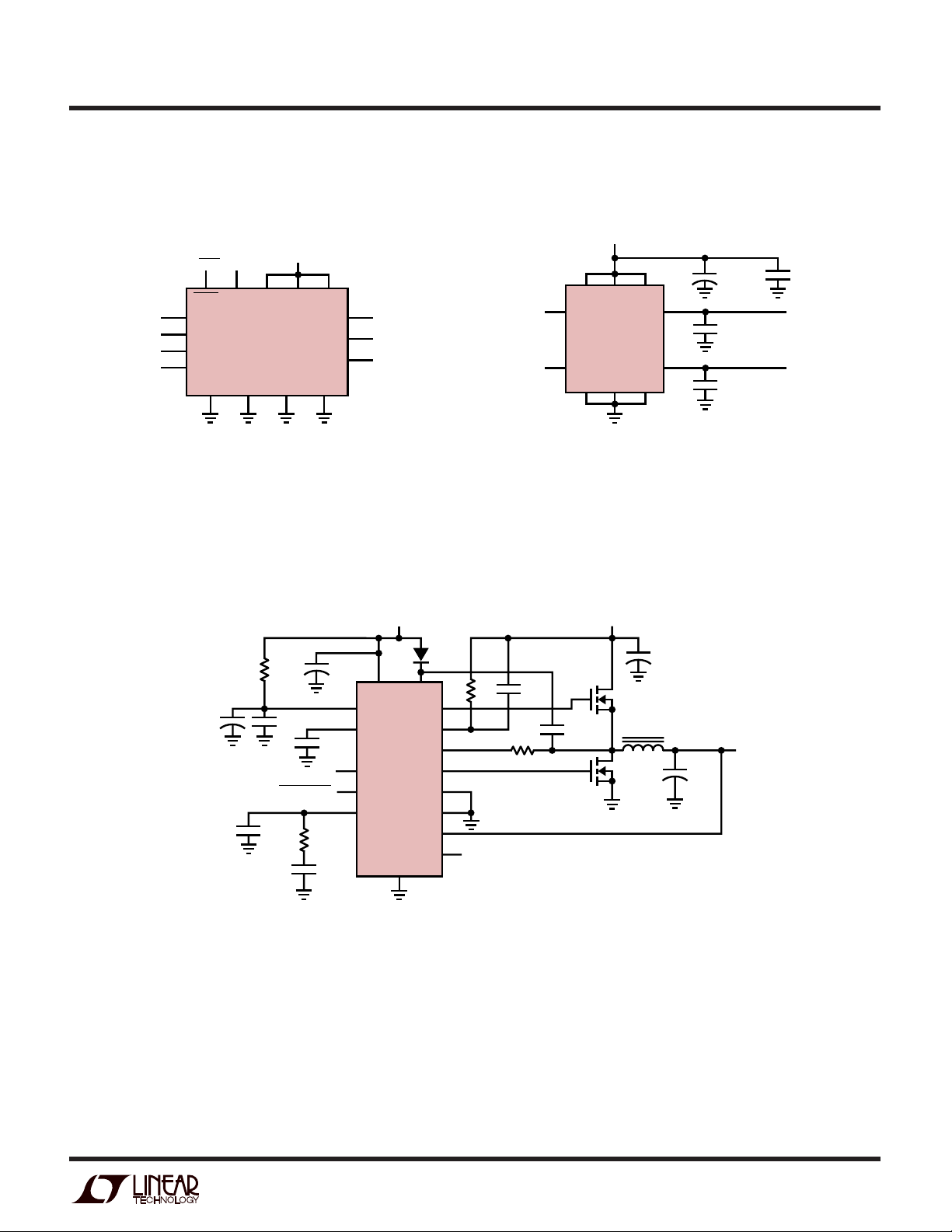
TEST CIRCUITS
V
SHDN
SHDN
NC
NC
NC
NC
I
MAX
FREQSET
COMP
SS
GND PGND SENSE
V
CC
V
CCPVCC2
LTC1430A
PV
SENSE
PV
CC
CC1IFB
–
LTC1430A
5V
+
10µF
PV
PV
V
CC1
CC
V
G1
G2
FB
NC
NC
NC
+
COMP
COMP
LTC1430A
V
FB
FB
GND
CC2
PGND
G1
10,000pF
G2
10,000pF
0.1µF
G1 RISE/FALL
G2 RISE/FALL
4.7µF
+
Figure 2
100Ω
0.1µF
SHUTDOWN
C1
220pF
+
0.01µF
R
C
7.5k
C
4700pF
1430 F02
1430 F03
Figure 3
V
CC
PV
CC1
I
MAX
PGND
GND
SENSE
–
1N4148
G1
I
FB
G2NC
+
FB NC
0.1µF
16k
1k
Q1A, Q1B, Q2: MOTOROLA MTD20N03HL
: AVX-TPSE227M010R0100
C
IN
C
: AVX-TPSE337M006R0100
OUT
1µF
PV
CC2
V
CC
SS
LTC1430A
FREQSET
SHDN
COMP
C
SENSE
0.1µF
V
= 5V
IN
Q1A, Q1B
2 IN PARALLEL
2.7µH/15A
Q2
+
C
IN
220µF
×4
+
C
OUT
330µF
×6
3.3V
1430 F04
Figure 4
7

LTC1430A
U
WUU
APPLICATIONS INFORMATION
OVERVIEW
T
he LTC1430A is a voltage feedback PWM switching
regulator controller (see Block Diagram) designed for use
in high power, low voltage step-down (buck) converters.
It includes an onboard PWM generator, a precision reference trimmed to ±0.5%, two high power MOSFET gate
drivers and all necessary feedback and control circuitry to
form a complete switching regulator circuit. The PWM
loop nominally runs at 200kHz.
The 16-lead versions of the LTC1430A include a current
limit sensing circuit that uses the upper external power
MOSFET as a current sensing element, eliminating the
need for an external sense resistor.
Also included in the 16-lead version is an internal soft start
feature that requires only a single external capacitor to
operate. In addition, 16-lead parts feature an adjustable
oscillator which can run at frequencies from 50kHz to
500kHz, allowing added flexibility in external component
selection. The 8-lead version does not include current
limit, internal soft start or frequency adjustability.
THEORY OF OPERATION
Primary Feedback Loop
The LTC1430A senses the output voltage of the circuit at
the output capacitor with the SENSE+ and SENSE– pins
and feeds this voltage back to the internal transconductance amplifier FB. FB compares the resistor-divided output voltage to the internal 1.265V reference and outputs an
error signal to the PWM comparator. This is then compared to a fixed frequency sawtooth waveform generated
by the internal oscillator to generate a pulse width modulated signal. This PWM signal is fed back to the external
MOSFETs through G1 and G2, closing the loop. Loop
compensation is achieved with an external compensation
network at COMP, the output node of the FB transconductance amplifier.
MIN, MAX Feedback Loops
Two additional comparators in the feedback loop provide
high speed fault correction in situations where the FB
amplifier may not respond quickly enough. MIN compares
the feedback signal to a voltage 40mV (3%) below the
internal reference. At this point, the MIN comparator
overrides the FB amplifier and forces the loop to full duty
cycle, set by the internal oscillator at about 93.5%. Similarly, the MAX comparator monitors the output voltage at
3% above the internal reference and forces the output to
0% duty cycle when tripped. These two comparators
prevent extreme output perturbations with fast output
transients, while allowing the main feedback loop to be
optimally compensated for stability.
Current Limit Loop
The 16-lead LTC1430A devices include yet another feedback loop to control operation in current limit. The current
limit loop is disabled in the 8-lead device. The I
fier monitors the voltage drop across external MOSFET Q1
with the IFB pin during the portion of the cycle when G1 is
high. It compares this voltage to the voltage at the I
As the peak current rises, the drop across Q1 due to its
R
that Q1’s drain current has exceeded the maximum level,
I
LIM
capacitor, cutting the duty cycle and controlling the output
current level. At the same time, the I
generates a signal to disable the MIN comparator to
prevent it from conflicting with the current limit circuit. If
the internal feedback node drops below about 0.8V, indicating a severe output overload, the circuitry will force the
internal oscillator to slow down by a factor of as much as
100. If desired, the turn on time of the current limit loop
can be controlled by adjusting the size of the soft start
capacitor, allowing the LTC1430A to withstand short
overcurrent conditions without limiting.
By using the R
the current limit circuit eliminates the sense resistor that
would otherwise be required and minimizes the number of
components in the external high current path. Because
power MOSFET R
with temperature, the LTC1430A current limit is not designed to be accurate; it is meant to prevent damage to the
power supply circuitry during fault conditions. The actual
current level where the limiting circuit begins to take effect
may vary from unit to unit, depending on the power
MOSFETs used. See Soft Start and Current Limit for more
details on current limit operation.
increases. When IFB drops below I
DS(ON)
starts to pull current out of the external soft start
of Q1 to measure the output current,
DS(ON)
is not tightly controlled and varies
DS(ON)
MAX
LIM
ampli-
LIM
pin.
MAX
, indicating
comparator
8
 Loading...