

Linear Technology LTC1422 Datasheet
FEATURES
■
Allows Safe Board Insertion and Removal
from a Live Backplane
■
System Reset Output with Programmable Delay
■
Programmable Electronic Circuit Breaker
■
User-Programmable Supply Voltage Power-Up Rate
■
High Side Driver for an External N-Channel FET
■
Controls Supply Voltages from 2.7V to 12V
■
Undervoltage Lockout
■
Soft Reset Input
■
Glitch Filter on RESET
U
APPLICATIO S
LTC1422
Hot Swap Controller
U
DESCRIPTIO
TM
The LTC®1422 is an 8-pin Hot Swap
allows a board to be safely inserted and removed from a
live backplane. Using an external N-channel pass transistor, the board supply voltage can be ramped up at a
programmable rate. A high side switch driver controls the
N-channel gate for supply voltages ranging from 2.7V to
12V.
A programmable electronic circuit breaker protects
against shorts. The RESET output can be used to generate
a system reset when the supply voltage falls below a
programmable voltage. The ON pin can be used to cycle
the board power or to generate a soft reset.
controller that
■
Hot Board Insertion
■
Electronic Circuit Breaker
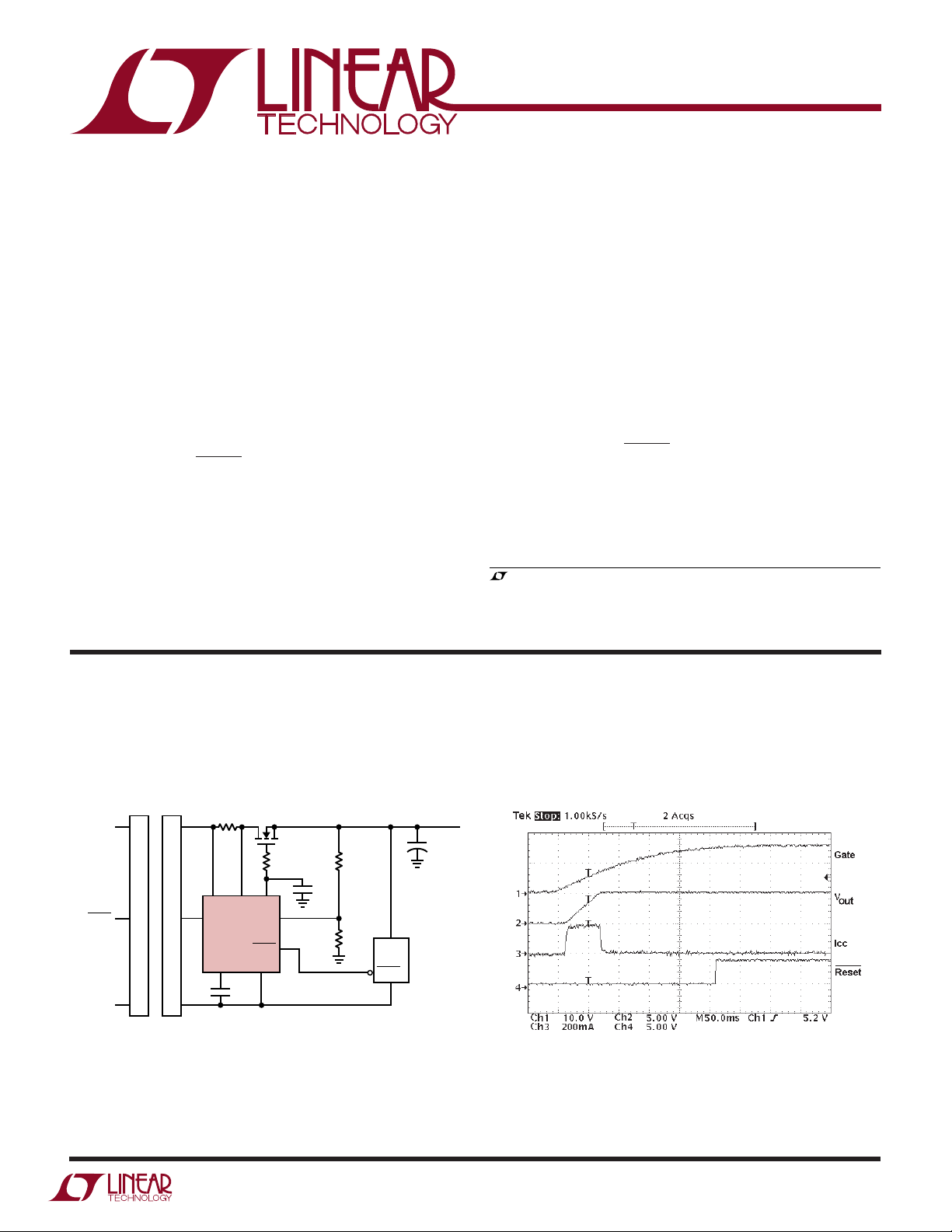
TYPICAL APPLICATIO
5V Hot Swap
Q1
R1
MTB50N06V
VCCSENSE GATE
ON
CONNECTOR 1
0.005Ω
R2
10Ω
5%
8
76
FB
LTC1422
RESET
GNDTIMER
34
C2
0.33µF
52
1
V
ON/RESET
GND
CC
CONNECTOR 2
PLUG-IN CARDBACKPLANE
U
C1
0.1µF
R3
6.81k
1%
R4
2.43k
1%
µP
RESET
The LTC1422 is available in 8-pin PDIP and SO packages.
, LTC and LT are registered trademarks of Linear Technology Corporation.
Hot Swap is a trademark of Linear Technology Corporation.
V
OUT
+
5V
C
LOAD
1422 TA01
1
LTC1422
1
2
3
4
8
7
6
5
TOP VIEW
N8 PACKAGE
8-LEAD PDIP
S8 PACKAGE
8-LEAD PLASTIC SO
RESET
ON
TIMER
GND
V
CC
SENSE
GATE
FB
WW
W
U
ABSOLUTE MAXIMUM RATINGS
PACKAGE
/
O
RDER I FOR ATIO
WU
(Note 1)
Supply Voltage (VCC) ........................................... 13.2V
Input Voltage (TIMER, SENSE) ... – 0.3V to (VCC + 0.3V)
Input Voltage (FB, ON)........................... –0.3V to 13.2V
Output Voltage (RESET) ........................ –0.3V to 13.2V
Output Voltage (GATE) ............................. –0.3V to 20V
Operating Temperature Range
ORDER PART
NUMBER
LTC1422CN8
LTC1422CS8
LTC1422IN8
LTC1422IS8
LTC1422C ............................................... 0°C to 70°C
T
LTC1422I........................................... –40°C to 85°C
Storage Temperature Range ................ –65°C to 150°C
Lead Temperature (Soldering, 10 sec)................. 300°C
Consult factory for Military grade parts.
ELECTRICAL CHARACTERISTICS
temperature range, otherwise specifications are at T
SYMBOL PARAMETER CONDITIONS MIN TYP MAX UNITS
DC Characteristics
I
CC
V
LKO
V
LKH
V
FB
∆V
V
FBHST
V
TM
∆V
V
TMHST
I
TM
V
CB
I
CP
∆V
V
ONHI
V
ONLO
V
ONHYST
V
OL
I
PU
t
RST
Note 1: Absolute Maximum Ratings are those values beyond which the life
of a device may be impaired.
VCC Supply Current ON = V
VCC Undervoltage Lockout ● 2.40 2.47 2.55 V
VCC Undervoltage Lockout Hysteresis 120 mV
FB Pin Voltage Threshold ● 1.220 1.232 1.244 V
FB Pin Threshold Line Regulation 3V ≤ V
FB
FB Pin Voltage Threshold Hysteresis 2.0 mV
TIMER Pin Voltage Threshold ● 1.208 1.232 1.256 V
TIMER Pin Threshold Line Regulation 3V ≤ VCC ≤ 12V ● 215 mV
TM
TIMER Pin Voltage Threshold Hystersis 45 mV
TIMER Pin Current Timer On, GND ≤ V
Timer Off, V
Circuit Breaker Trip Voltage VCB = (VCC – V
GATE Pin Output Current Charge Pump On, V
Charge Pump Off, V
External N-Channel Gate Drive V
GATE
ON Pin Threshold High ● 1.25 1.30 1.35 V
ON Pin Threshold Low ● 1.20 1.23 1.26 V
ON Pin Hysteresis 80 mV
Output Low Voltage RESET, IO = 3mA ● 0.14 0.4 V
Logic Output Pull-Up Current RESET = GND –12 µA
Soft Reset Time ● 22 30 38 µs
GATE
The ● denotes the specifications which apply over the full operating
= 25°C. V
A
CC
≤ 12V ● 0.5 2.5 mV
CC
– V
CC
= 5V unless otherwise noted.
CC
≤ 1.5V ● –2.5 –2.0 –1.5 µA
TIMER
= 1.5V 10 mA
TIMER
) ● 44 50 64 mV
SENSE
= GND ● –12 –10 –8 µA
GATE
= V
GATE
= 150°C, θJA = 130°C/W (N)
JMAX
= 150°C, θJA = 150°C/W (S)
T
JMAX
CC
S8 PART MARKING
1422
1422I
● 0.65 1.00 mA
10 mA
● 10 12 14 V
2
U
UW
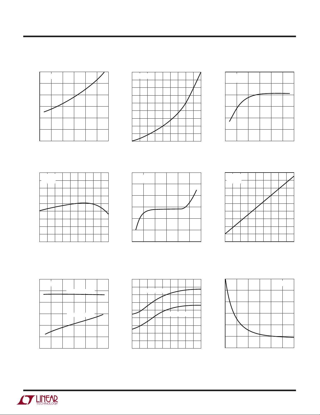
TYPICAL PERFORMANCE CHARACTERISTICS
LTC1422
Supply Current vs Supply Voltage Supply Current vs Temperature
1200
TA = 25°C
1000
800
600
400
SUPPLY CURRENT (µA)
200
0
2
6810
4
SUPPLY VOLTAGE (V)
Gate Voltage vs Temperature
18.2
VCC = 5V
= 0A
I
18.0
G
17.8
17.6
17.4
17.2
17.0
GATE VOLTAGE (V)
16.8
16.6
16.4
–55
–35
5
–15
25
TEMPERATURE (°C)
45
12 14
1422 G01
125
85
105
65
1422 G04
775
VCC = 5V
750
725
700
675
650
625
SUPPLY CURRENT (µA)
600
575
550
–55
–35
5
–15
25
TEMPERATURE (°C)
45
Gate Current vs Supply Voltage
16
TA = 25°C
= 0V
V
G
14
12
10
8
GATE CURRENT (µA)
6
4
2
6810
4
SUPPLY VOLTAGE (V)
Gate Voltage vs Supply Voltage
30
TA = 25°C
= 0A
I
G
25
20
15
10
GATE VOLTAGE (V)
5
0
125
85
105
65
1422 G02
2
6810
4
SUPPLY VOLTAGE (V)
12 14
1422 G03
Gate Current vs Temperature
10.4
VCC = 5V
= 0V
V
10.2
G
10.0
9.8
9.6
9.4
9.2
GATE CURRENT (µA)
9.0
8.8
12 14
1422 G05
8.6
–55
–35
–15
5
25
45
TEMPERATURE (°C)
65
125
85
105
1422 G06
Feedback Threshold Voltage
vs Supply Voltage
1.2350
TA = 25°C
1.2345
1.2340
1.2335
1.2330
1.2325
FEEDBACK THRESHOLD VOLTAGE (V)
1.2320
2
4
HIGH THRESHOLD
LOW THRESHOLD
6810
SUPPLY VOLTAGE (V)
12 14
1422 G07
Feedback Threshold Voltage
vs Temperature
1.237
1.236
1.235
1.234
1.233
1.232
1.231
1.230
1.229
FEEDBACK THRESHOLD VOLTAGE (V)
1.228
HIGH THRESHOLD
–55
–35
5
–15
25
TEMPERATURE (°C)
LOW THRESHOLD
45
Glitch Filter Time
vs Feedback Transient
70
60
50
40
30
GLITCH FILTER TIME (µs)
20
10
65
125
85
105
1422 G08
0
80 120 160
40
FEEDBACK TRANSIENT (mV)
TA = 25°C
200 240
1422 G09
3
LTC1422
UW
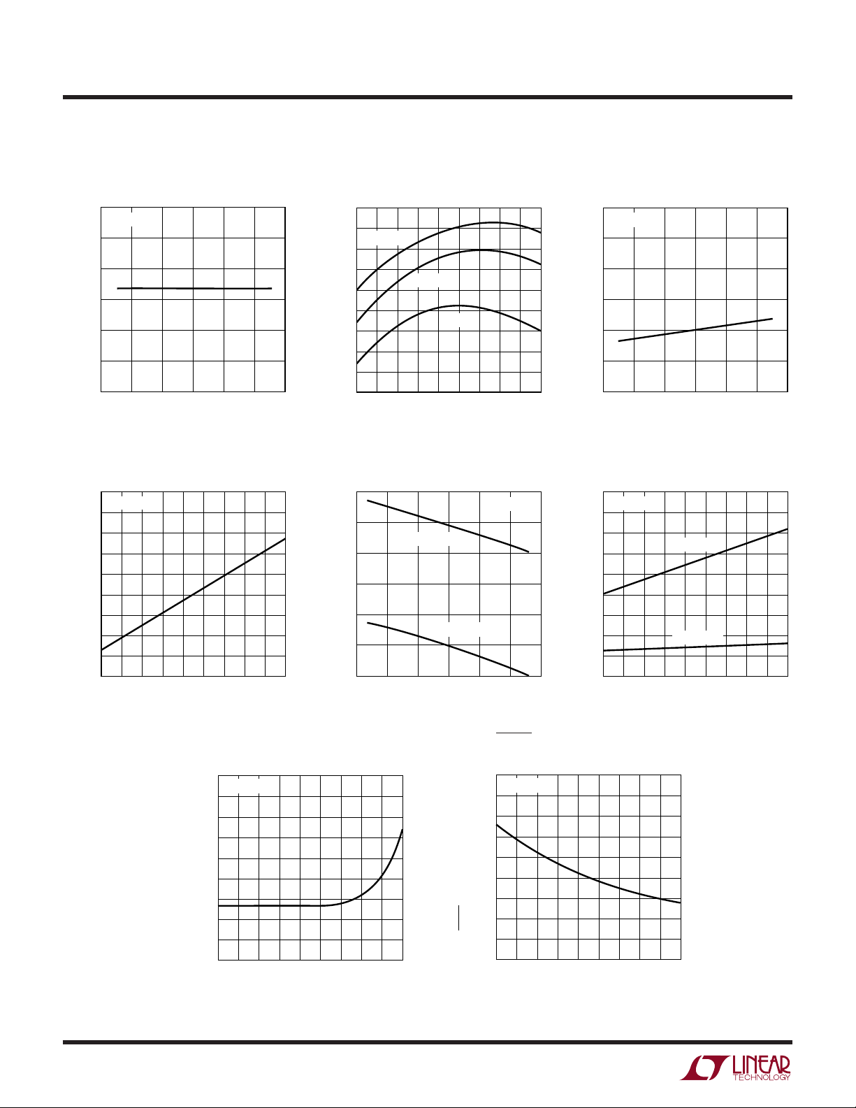
TYPICAL PERFORMANCE CHARACTERISTICS
TIMER Threshold Voltage
vs Supply Voltage
1.244
TA = 25°C
1.242
1.240
1.238
1.236
1.234
TIMER THRESHOLD VOLTAGE (V)
1.232
2
2.45
VCC = 5V
2.40
2.35
2.30
2.25
2.20
2.15
TIMER CURRENT (µA)
2.10
2.05
2.00
–55
–35
6810
4
SUPPLY VOLTAGE (V)
5
–15
25
TEMPERATURE (°C)
TIMER Threshold Voltage
vs Temperature
1.242
12 14
1422 G10
1.241
1.240
1.239
1.238
1.237
1.236
1.235
TIMER THRESHOLD VOLTAGE (V)
1.234
1.233
–55
VCC = 12V
–35
–15
VCC = 5V
VCC = 3V
5
25
45
TEMPERATURE (°C)
65
125
85
105
1422 G11
ON Pin Threshold Voltage
vs Supply VoltageTIMER Current vs Temperature
1.32
1.30
2
HIGH THRESHOLD
LOW THRESHOLD
6810
4
SUPPLY VOLTAGE (V)
1.28
1.26
1.24
1.22
ON PIN THRESHOLD VOLTAGE (V)
45
65
125
85
105
1422 G13
1.20
TA = 25°C
12 14
1422 G14
TIMER Current vs Supply Voltage
2.6
TA = 25°C
2.5
2.4
2.3
2.2
TIMER CURRENT (µA)
2.1
2.0
2
6810
4
SUPPLY VOLTAGE (V)
ON Pin Threshold Voltage
vs Temperature
1.38
VCC = 5V
1.36
1.34
1.32
1.30
1.28
1.26
1.24
ON PIN THRESHOLD VOLTAGE (V)
1.22
1.20
–55
–35
INPUT HIGH
INPUT LOW
5
–15
25
TEMPERATURE (°C)
45
12 14
1422 G12
65
125
85
105
1422 G15
4
Current Limit Threshold
vs Temperature
85
VCC = 5V
80
75
70
65
60
55
50
CURRENT LIMIT THRESHOLD (mV)
45
40
–35
–55
5
–15
25
TEMPERATURE (°C)
45
RESET Pull-Up Current
vs Temperature
22
VCC = 5V
20
18
16
14
12
10
8
RESET PULL-UP CURRENT (µA)
6
4
–35
125
85
105
65
1422 G17
–55
5
–15
25
TEMPERATURE (°C)
45
65
125
85
105
1422 G18
UW
TYPICAL PERFORMANCE CHARACTERISTICS
RESET Voltage vs Temperature
0.24
VCC = 5V
0.22
3mA PULL-UP
0.20
0.18
0.16
0.14
0.12
RESET VOLTAGE (V)
0.10
0.08
0.06
–55
–35
–15
5
25
45
TEMPERATURE (°C)
65
125
85
105
1422 G19
55
50
45
40
35
30
25
ON PIN PULSE TIME (µs)
20
15
10
UUU
PIN FUNCTIONS
ON Pin Pulse (Soft Reset) Time
vs Temperature
VCC = 3V
VCC = 5V
VCC = 12V
5
25
–55
–35
–15
TEMPERATURE (°C)
45
65
85
LTC1422
125
105
1422 G20
RESET (Pin 1) : Open drain output to GND with a 12µA
pull-up to VCC. This pin is pulled low when the voltage at
the FB (Pin 5) goes below the FB pin threshold. The RESET
pin will go high one timing cycle after the voltage at the FB
pin goes above the FB pin threshold. An external pull-up
resistor can be used to speed up the rising edge on the
RESET pin or pull the pin to a voltage higher or lower than
VCC.
ON (Pin 2): Analog Input Pin. The threshold is set at 1.30V
with 80mV hysteresis. When the ON pin is pulled high, the
timer turns on for one cycle, then the charge pump turns
on. When the ON pin is pulled low longer than 40µs, the
GATE pin will be pulled low and remain off until the ON pin
is pulled high.
If the ON pin is pulled low for less than 15µs a soft reset
will occur. The charge pump remains on, and the RESET
pin is pulled low for one timing cycle starting 30µs from
the falling edge of the ON pin.
The ON pin is also used to reset the electronic circuit
breaker. If the ON pin is cycled low and high following the
trip of the circuit breaker, the circuit breaker is reset and
a normal power-up sequence will occur.
TIMER (Pin 3): Analog system timing generator pin. This
pin is used to set the delay before the charge pump turns
on after the ON pin goes high. It also sets the delay before
the RESET pin goes high, after the output supply voltage
is good, as sensed by the FB pin.
When the timer is off, an internal N-channel shorts the
TIMER pin to ground. When the timer is turned on, a 2µA
current from VCC is connected to the TIMER pin and the
voltage starts to ramp up with a slope given by: dV/dt =
2µA/C
. When the voltage reaches the trip point
TIMER
(1.232V), the timer will be reset by pulling the TIMER pin
back to ground. The timer period is given by: (1.232V •
C
TIMER
)/2µA.
GND (Pin 4): Chip Ground.
FB (Pin 5): Analog comparator input used to monitor the
output supply voltage with an external resistive divider.
When the voltage on the FB pin is lower than the 1.232V,
the RESET pin will be pulled low. An internal filter helps
prevent negative voltage glitches from triggering a reset.
When the voltage on the FB pin rises above the trip point,
the RESET pin will go high after one timing cycle.
5
 Loading...