

Linear Technology LTC1421ISW-2.5, LTC1421ISW, LTC1421IG-2.5, LTC1421CSW, LTC1421CG-2.5 Datasheet
...
1
LTC1421/LTC1421-2.5
Hot Swap Controller
■
Allows Safe Board Insertion and Removal from a
Live Backplane
■
System Reset and Power Good Control Outputs
■
Programmable Electronic Circuit Breaker
■
User Programmable Supply Voltage Power-Up Rate
■
High Side Driver for Two External N-Channels
■
Controls Supply Voltages from 3V to 12V
■
Connection Inputs Detect Board Insertion or Removal
■
Undervoltage Lockout
■
Power-On Reset Input
■
Hot Board Insertion
■
Electronic Circuit Breaker
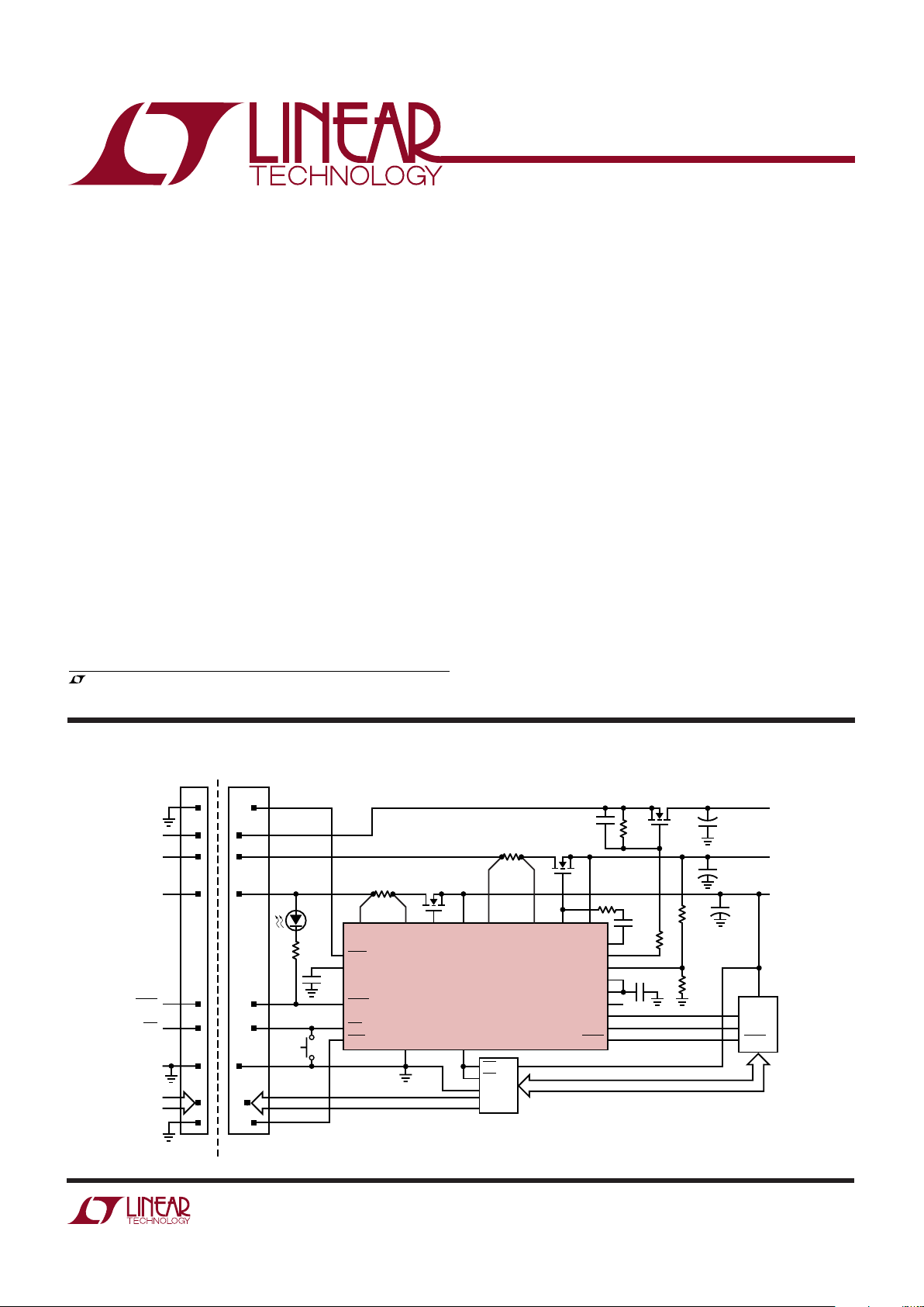
The LTC®1421/LTC1421-2.5 are Hot Swap
TM
controllers
that allow a board to be safely inserted and removed from a
live backplane. Using external N-channel pass transistors,
the board supply voltages can be ramped up at a programmable rate. Two high side switch drivers control the Nchannel gates for supply voltages ranging from 3V to 12V.
A programmable electronic circuit breaker protects against
shorts. Warning signals indicate that the circuit breaker
has tripped, a power failure has occurred or that the switch
drivers are turned off. The reset output can be used to
generate a system reset when the power cycles or a fault
occurs. The two connect inputs can be used with staggered connector pins to indicate board insertion or removal. The power-on reset input can be used to cycle the
board power or clear the circuit breaker.
The trip point of the ground sense comparator is set at
0.1V for LTC1421 and 2.5V for LTC1421-2.5.
The LTC1421/LTC1421-2.5 are available in 24-pin SO and
SSOP packages.
10
9
14
13
8
11
15
6
7
RAMP
CPON
COMP
–
COMP
+
REF
FB
COMPOUT
PWRGD
RESET
2
24
4
3
1
CON2
AUXV
CC
FAULT
POR
CON1
V
CCLO
SETLO GATELO V
OUTLO
LTC1421
GND DISABLE
V
CCHI
SETHI GATEHI V
OUTHI
16
C2
0.1µF
C1
1µF
R5
16k
5%
Q1
MTB50N06E
R1
0.005Ω
171819202122
512
23
R3
1k
STAGGERED CONNECTOR
D1
R6
20k
1%
R4
20k
5%
R7
7.15k
1%
Q2
1/2 Si4936DY
Q3
1/2 Si4936DY
C3
0.47µF
R2
0.025Ω
+
C
LOAD
C
LOAD
C
LOAD
V
EE
–12V
1A
V
DD
12V
1A
V
CC
5V
5A
+
+
I/O
I/O
RESET
BEA
BEB
GND
1
13
12
µP
QS3384
QuickSwitch
®
QuickSwitch IS A REGISTERED TRADEMARK
OF QUALITY SEMICONDUCTOR CORPORATION.
1421 TA01
DATA BUS
PC BOARDBACKPLANE
DATA
BUS
GND
POR
FAULT
V
CC
V
DD
V
EE
V
CC
1µF
43
21
43
21
10k
, LTC and LT are registered trademarks of Linear Technology Corporation.
Hot Swap is a trademark of Linear Technology Corporation.
DESCRIPTIO
U
FEATURES
APPLICATIO S
U
TYPICAL APPLICATIO
U
2
LTC1421/LTC1421-2.5
ABSOLUTE MAXIMUM RATINGS
W
WW
U
WU
U
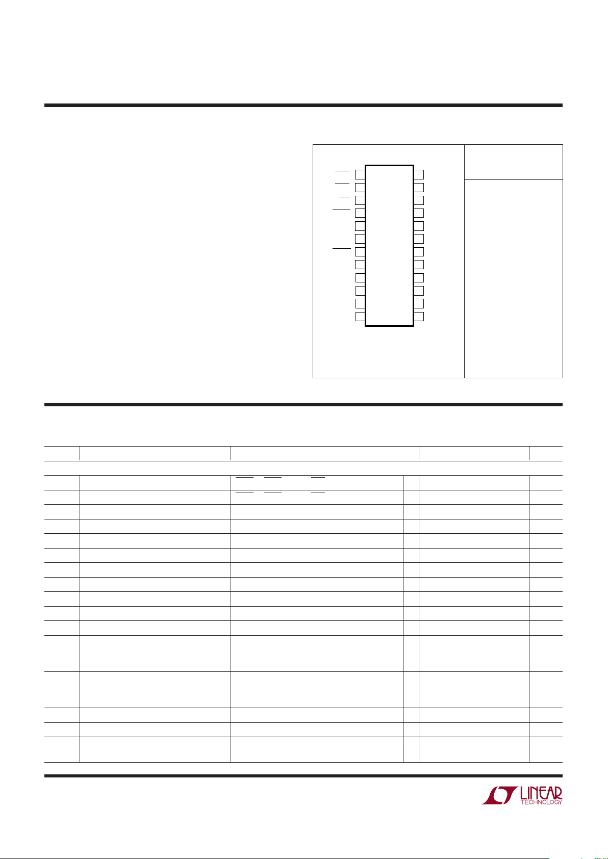
PACKAGE
/
O
RDER I FOR ATIO
Consult factory for parts specified with wider operating temperature ranges.
(Note 1)
Supply Voltage (V
CCLO, VCCHI
, AUXVCC) .............. 13.2V
Input Voltage (Analog Pins)..... – 0.3V to (V
CCHI
+ 0.3V)
Input Voltage (Digital Pins)................... – 0.3V to 13.2V
Output Voltage (Digital Pins) .. – 0.3V to (V
CCLO
+ 0.3V)
Output Voltage (CPON)......... – 13.2V to (V
CCLO
+ 0.3V)
Output Voltage (V
OUTLO
, V
OUTHI
) ........... –0.3V to 13.2V
Output Voltage (GATELO, GATEHI)........... –0.3V to 20V
Operating Temperature Range
LTC1421C ............................................... 0°C to 70°C
LTC1421I........................................... –40°C to 85°C
Storage Temperature Range ................ –65°C to 150°C
Lead Temperature (Soldering, 10 sec)................. 300°C
ORDER PART
NUMBER
T
JMAX
= 125°C, θJA = 100°C/W (G)
T
JMAX
= 125°C, θJA = 85°C/W (SW)
1
2
3
4
5
6
7
8
9
10
11
12
TOP VIEW
SW PACKAGE
24-LEAD PLASTIC SO
G PACKAGE
24-LEAD PLASTIC SSOP
24
23
22
21
20
19
18
17
16
15
14
13
CON1
CON2
POR
FAULT
DISABLE
PWRGD
RESET
REF
CPON
RAMP
FB
GND
AUXV
CC
V
CCLO
SETLO
GATELO
V
OUTLO
V
CCHI
SETHI
GATEHI
V
OUTHI
COMPOUT
COMP
–
COMP
+
ELECTRICAL CHARACTERISTICS
The ● denotes specifications which apply over the full operating
temperature range, otherwise specifications are at TA = 25°C. V
CCHI
= 12V, V
CCLO
= 5V unless otherwise noted (Note 2).
SYMBOL PARAMETER CONDITIONS MIN TYP MAX UNITS
DC Characteristics
I
CCLO
V
CCLO
Supply Current CON1 = CON2 = GND, POR = V
CCLO
● 1.5 3 mA
I
CCHI
V
CCHI
Supply Current CON1 = CON2 = GND, POR = V
CCLO
● 0.6 1 mA
V
LKO
Undervoltage Lockout V
CCLO
and V
CCHI
2.28 2.45 2.60 V
V
LKH
Undervoltage Lockout Hysteresis V
CCLO
and V
CCHI
100 mV
V
REF
Reference Output Voltage No Load ● 1.220 1.232 1.244 V
∆V
LNR
Reference Line Regulation 3V ≤ V
CCLO
≤ 12V, No Load ● 48 mV
∆V
LDR
Reference Load Regulation IO = 0mA to –5mA, Sourcing Only ● 13 mV
I
RSC
Reference Short-Circuit Current V
REF
= 0V –45 mA
V
COF
Comparator Offset Voltage 0V ≤ V
CM
≤ (V
CCLO
− 1.3V) ● ±10 mV
V
CPSR
Comparator Power Supply Rejection 0V ≤ V
CM
≤ (V
CCLO
− 1.3V), 3V ≤ V
CCLO
≤ 12V ● 1 mV/V
V
CHST
Comparator Hysteresis 0V ≤ V
CM
≤ (V
CCLO
− 1.3V) 7 mV
V
RST
Reset Voltage Threshold (V
OUTLO
) FB = V
OUTLO
● 2.80 2.90 3.00 V
FB = Floating
● 4.50 4.65 4.75 V
FB = GND
● 5.75 5.88 6.01 V
V
RHST
Reset Threshold Hysteresis (V
OUTLO
) FB = V
OUTLO
7mV
FB = Floating 12 mV
FB = GND 15 mV
R
FB
FB Pin Input Resistance 0V ≤ V
FB
≤ V
CCLO
95 kΩ
V
CB
Circuit Breaker Trip Voltage V
CB
= (V
CCLO
– V
SETLO
) or V
CB
= (V
CCHI
– V
SETHI
) ● 40 50 60 mV
V
TRIP
Output Voltage for Re-Power-Up LTC1421 (Note 3) 0.1 V
LTC1421-2.5 (Note 4) 2.5 V
LTC1421CG
LTC1421CSW
LTC1421CG-2.5
LTC1421CSW-2.5
LTC1421IG
LTC1421ISW
LTC1421IG-2.5
LTC1421ISW-2.5
3
LTC1421/LTC1421-2.5
Note 3: After power-on reset, the V
OUTLO
and V
OUTHI
have to drop below the
V
TRIP
point before the charge pump is restarted.
Note 4: After power-on reset, the V
OUTLO
has to drop below the V
TRIP
point
before the charge pump is restarted.
Note 1: Absolute Maximum Ratings are those values beyond which the life
of a device may be impaired.
Note 2: All currents into device pins are positive; all currents out of device
pins are negative. All voltages are reference to ground unless otherwise
specified.
ELECTRICAL CHARACTERISTICS
The ● denotes specifications which apply over the full operating
temperature range, otherwise specifications are at TA = 25°C. V
CCHI
= 12V, V
CCLO
= 5V unless otherwise noted (Note 2).
SYMBOL PARAMETER CONDITIONS MIN TYP MAX UNITS
I
RAMP
RAMP Pin Output Current Charge Pump On, V
RAMP
= 0.4V ● 11 17 23 µA
I
CP
Charge Pump Output Current Charge Pump On, GATEHI = 0V –600 µA
GATELO = 0V –300 µA
∆V
GATEHI
GATEHI N-Channel Gate Drive V
GATEHI
− V
OUTHI
616V
∆V
GATELO
GATELO N-Channel Gate Drive V
GATELO
− V
OUTLO
10 16 V
V
AUXVCC
Auxiliary VCC Output Voltage V
CCLO
= 5V, Unloaded 4.5 V
V
IL
Input Low Voltage CON1, CON2, POR ● 0.8 V
V
IH
Input High Voltage CON1, CON2, POR ● 2V
I
IN
Input Current CON1, CON2, POR = GND ● –30 –60 –90 µA
V
OL
Output Low Voltage RESET, COMPOUT, PWRGD, DISABLE, FAULT, ● 0.4 V
I
O
= 3mA
CPON, IO = 3mA ● 1.45 V
V
OH
Output High Voltage DISABLE, IO = –3mA ● 4V
CPON, IO = –1mA ● 3.4 V
I
PU
Logic Output Pull-Up Current RESET, PWRGD, FAULT = GND –15 µA
AC CHARACTERISTICS
t
1
CON1 or CON2↓ to CPON↑ Figure 1, CL = 15pF ● 15 20 30 ms
t
2
PWRGD↑ to RESET↑ Figure 1, RL = 10k to V
CCLO
, CL = 15pF 160 200 240 ms
● 140 200 280 ms
t
3
PWRGD↑ to DISABLE↓ Figure 1, CL = 15pF 160 200 240 ms
● 140 200 280 ms
t
4
POR↓ to CPON↓ Figure 1, CL = 15pF ● 15 20 30 ms
t
5
PWRGD↓ to RESET↓ Figure 1, RL = 10k to V
CCLO
, CL = 15pF 32 µs
t
6
POR↑ to CPON↑ Figure 1, CL = 15pF 50 ns
t
7
CON1 or CON2↑ to CPON↓ Figure 1, CL = 15pF 50 ns
t
9
Short-Circuit Detect to FAULT↓ Figure 1, RL = 10k to V
CCLO
, CL = 15pF 20 µs
V
CCLO
– SETLO = 0mV to 100mV
t
10
Short-Circuit Detect to CPON↓ Figure 2, CL = 15pF 20 µs
V
CCLO
– SETLO = 0mV to 100mV
t
11
POR↑ to FAULT↑ Figure 2, RL = 10k to V
CCLO
, CL = 15pF 20 ns
t
CHL
Comparator High to Low COMP– = 1.232V, 10mV Overdrive ● 0.25 0.5 µs
R
L
= 10k to V
CCLO
, CL = 15pF
t
CLH
Comparator Low to High COMP– = 1.232V, 10mV Overdrive ● 1 1.5 µs
R
L
= 10k to V
CCLO
, CL = 15pF
4
LTC1421/LTC1421-2.5
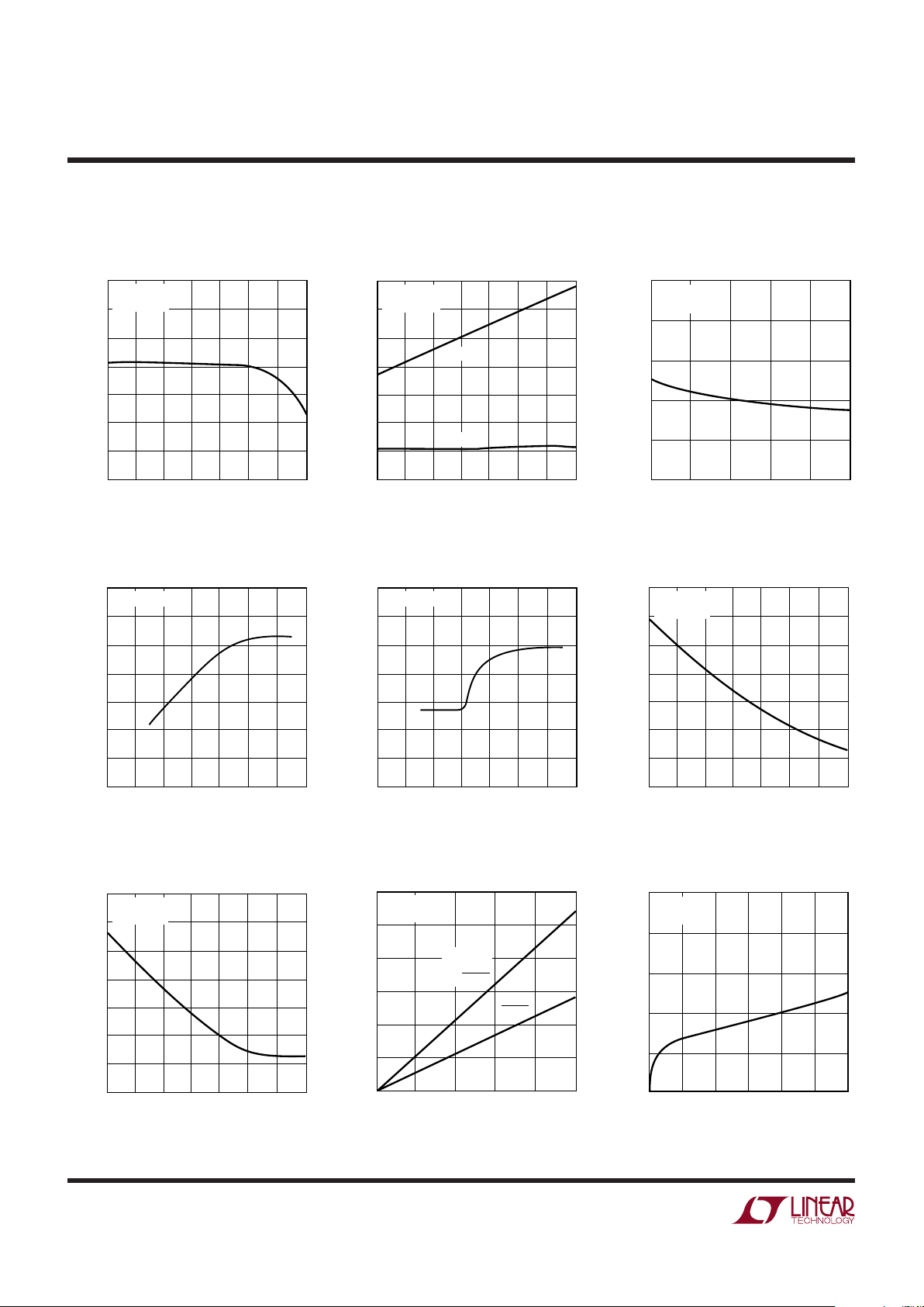
TYPICAL PERFORMANCE CHARACTERISTICS
U
W
TEMPERATURE (°C)
–50
1.232
1.234
1.238
25 75
1421 G01
1.230
1.228
–25 0
50 100 125
1.226
1.224
1.236
REFERENCE VOLTAGE (V)
V
CCLO
= 5V
V
CCHI
= 12V
Reference Voltage vs
Temperature
SOURCE CURRENT (mA)
0
REFERENCE VOLTAGE (V)
1.235
1.240
1.245
8
1421 G03
1.230
1.225
1.220
2
4
6
10
V
CCLO
= 5V
V
CCHI
= 12V
Reference Voltage
vs Source CurrentGate Voltage vs Temperature
TEMPERATURE (°C)
–50
21
22
24
25 75
1421 G02
20
19
–25 0
50 100 125
18
17
23
GATE VOLTAGE (V)
V
CCLO
= 5V
V
CCHI
= 12V
GATEHI
GATELO
GATELO Voltage vs V
CCLO
Voltage
V
CCLO
VOLTAGE (V)
0
20
22
26
610
1421 G04
18
16
24
81214
14
12
24
GATELO VOLTAGE (V)
V
CCHI
= 12V
GATEHI Voltage vs V
CCHI
Voltage
V
CCHI
VOLTAGE (V)
0
20
22
26
610
1421 G05
18
16
24
81214
14
12
24
GATEHI VOLTAGE (V)
V
CCLO
= 5V
I
CCLO
Supply Current
vs Temperature
TEMPERATURE (°C)
–50
1400
25 75
1421 G06
1300
–25 0
50 100 125
1200
1500
I
CCLO
SUPPLY CURRENT (µA)
V
CCLO
= 5V
V
CCHI
= 12V
VOL vs I
SINK
CPON Voltage vs Sink Current
(Charge Pump Off)
I
CCHI
Supply Current
vs Temperature
TEMPERATURE (°C)
–50
540
25 75
1421 G07
530
–25 0
50 100 125
520
550
545
535
525
555
I
CCHI
SUPPLY CURRENT (µA)
V
CCLO
= 5V
V
CCHI
= 12V
SINK CURRENT (mA)
0
0
VOLTAGE (mV)
100
200
300
400
500
FAULT
600
2468
1421 G08
10
V
CCLO
= 5V
V
CCHI
= 12V
COMPOUT
PWRGD
RESET
SINK CURRENT (mA)
0
0
CPON VOLTAGE (V)
0.5
1.0
1.5
2.0
2.5
0.5
1.0 1.5 2.0
1421 G09
2.5 3.0
V
CCLO
= 5V
V
CCHI
= 12V
5
LTC1421/LTC1421-2.5
TYPICAL PERFORMANCE CHARACTERISTICS
U
W
CPON Voltage vs Source Current
(Charge Pump On)
SOURCE CURRENT (mA)
0
0
CPON VOLTAGE (V)
1
2
3
4
5
–0.5
–1.0 –1.5 –2.0
1421 G10
–2.5 –3.0
V
CCLO
= 5V
V
CCHI
= 12V
I
CCLO
Supply Current
vs V
CCLO
Voltage
V
CCLO
VOLTAGE (V)
0
4
5
7
610
1421 G11
3
2
24
81214
1
0
6
I
CCLO
SUPPLY CURRENT (mA)
V
CCHI
= 12V
PIN FUNCTIONS
UUU
CON1 (Pin 1): TTL Level Input with a Pull-Up to V
CCLO
.
Together with CON2, it is used to indicate board connection. The pin must be tied to ground on the host side of the
connector. When using staggered connector pins, CON1
and CON2 must be the shortest and must be placed at
opposite corners of the connector. Board insertion is
assumed after CON1 and CON2 are both held low for 20ms
after power-up.
CON2 (Pin 2):
TTL Level Input with a Pull-Up to V
CCLO
.
Together with CON1 it is used to indicate board connection.
POR (Pin 3): TTL Level Input with a Pull-Up to V
CCLO
.
When the pin is pulled low for at least 20ms, a hard reset
is generated. Both V
OUTLO
and V
OUTHI
will turn off at a
controlled rate. A power-up sequence will not start until
the POR pin is pulled high. If POR is pulled high before
V
OUTLO
and V
OUTHI
are fully discharged, a power-up
sequence will not begin until the voltage at V
OUTLO
and
V
OUTHI
are below V
TRIP
. The electronic circuit breaker will
be reset by pulling POR low.
FAULT (Pin 4): Open Drain Output to GND with a Weak
Pull-Up to V
CCLO
. The pin is pulled low when an overcur-
rent fault is detected at V
OUTLO
or V
OUTHI
.
DISABLE (Pin 5): CMOS Output. The signal is used to
disable the board’s data bus during insertion or removal.
PWRGD (Pin 6): Open Drain Output to GND with a Weak
Pull-Up to V
CCLO
. The pin is pulled low immediately after
V
OUTLO
falls below its reset threshold voltage. The pin is
pulled high immediately after V
OUTLO
rises above its reset
threshold voltage.
RESET (Pin 7):
Open Drain Output to GND with a Weak
Pull-Up to V
CCLO
. The pin is pulled low when a reset
condition is detected. A reset will be generated when any
of the following conditions are met: Either CON1 or CON2
is high, POR is pulled low, V
CCLO
or V
CCHI
are below their
respective undervoltage lockout thresholds, PWRGD goes
low or an overcurrent fault is detected at V
OUTLO
or
V
OUTHI
. RESET will go high 200ms after PWRGD goes
high. On power failure, RESET will go low 32µs after
PWRGD goes low.
REF (Pin 8): The Reference Voltage Output. V
OUT
= 1.232V
±1%. The reference can source up to 5mA of current. A
1µF bypass capacitor is recommended.
CPON (Pin 9): CMOS Output That Can Be Pulled Below
Ground. CPON is pulled high when the internal charge
pumps for GATELO and GATEHI are turned on. CPON is
pulled low when the charge pumps are turned off. The pin
can be used to control an external MOSFET for a –5V to
–12V supply.

6
LTC1421/LTC1421-2.5
PIN FUNCTIONS
UUU
RAMP (Pin 10): Analog Power-Up Ramp Control Pin. By
connecting an external capacitor between the RAMP and
GATEHI, a positive linear voltage ramp on GATEHI and
GATELO is generated on power-up with a slope equal to
20µA/C
RAMP
. A 10k resistor in series with the capacitor
enhances the ESD performance at the GATEHI pin.
FB (Pin 11): Analog Feedback Input. FB is used to set the
reset threshold voltage on V
CCLO
. For a 5V supply leave FB
floating. For a 3.3V supply, short FB to V
CCLO
.
GND (Pin 12): Ground
COMP+ (Pin 13): Noninverting Comparator Input.
COMP– (Pin 14): Inverting Comparator Input.
COMPOUT (Pin 15): Open Drain Comparator Output.
V
OUTHI
(Pin 16): High Supply Voltage Output. This must be
the higher of the two supply voltage outputs.
GATEHI (Pin 17): The High Side Gate Drive for the High
Supply N-Channel. An internal charge pump guarantees at
least 6V of gate drive. The slope of the voltage rise at
GATEHI is set by the external capacitor connected between
GATEHI and RAMP. When the circuit breaker trips, GATEHI
is immediately pulled to GND.
SETHI (Pin 18): The Circuit Breaker Set Pin for the High
Supply. With a sense resistor placed in the supply path
between V
CCHI
and SETHI, the circuit breaker will trip when
the voltage across the resistor exceeds 50mV for more
than 20µs. To disable the circuit breaker, V
CCHI
and SETHI
should be shorted together.
V
CCHI
(Pin 19): The Positive Supply Input. This must be the
higher of the two input supply voltages. An undervoltage
lockout circuit disables the chip until the voltage at V
CCHI
is greater than 2.45V.
V
OUTLO
(Pin 20): Low Supply Voltage Output. This must be
the lower of the two supply voltage outputs.
GATELO (Pin 21): The High Side Gate Drive for the Low
Supply N-Channel Pass Transistor. An internal charge
pump guarantees at least 10V of gate drive. The slope of
the voltage rise at GATELO is set by the external capacitor
connected between GATEHI and RAMP. When the circuit
breaker trips GATELO is immediately pulled to GND.
SETLO (Pin 22): The Circuit Breaker Set Pin for the Low
Supply. With a sense resistor placed in the supply path
between V
CCLO
and SETLO, the circuit breaker will trip
when the voltage across the resistor exceeds 50mV for
more than 20µs. To disable the circuit breaker, V
CCLO
and
SETLO should be shorted together.
V
CCLO
(Pin 23): The Positive Supply Input. V
CCLO
must be
equal to or lower voltage than V
CCHI
. An undervoltage
lockout circuit disables the chip until the voltage at V
CCLO
is greater than 2.45V.
AUXVCC (Pin 24): The supply input for the GATELO and
GATEHI discharge circuitry. Connect a 1µF capacitor to
ground. AUXVCC is powered from V
CCLO
via an internal
Schottky diode and series resistor.

7
LTC1421/LTC1421-2.5
BLOCK DIAGRAM
W
Figure 1. Nominal Operation Switching Waveforms
Figure 2. Fault Detection Switching
CPON
CON1
t
1
CON2
RESET
DISABLE
POR
1421 F01
PWRGD
t
2
t
3
t
4
t
6
t
5
t
7
CPON
V
CCLO
– SETLO
t
9
FAULT
RESET
POR
1421 F02
PWRGD
t
2
t
5
t
11
t
6
t
10
SWITCHI G TI E WAVEFOR S
UW W
–
+
+
–
+
+
–
V
TRIP
+
–
+
–
50mV50mV
CPON
AUXV
CC
V
CCHI
SETLO
CP1 CP2
V
CCLO
SETHI GATELO RAMP GATEHI V
OUTHI
V
OUTLO
192223 18 21 10 17 16 20
V
CC
FAULT
CON1
CON2
POR
DISABLE
9
24
4
1
2
3
5
20µA
V
CC
CP3
CP4
CP5
73.5k
N1N2
AUXV
CC
FB
REF
11
8
PWRGD
6
RESET
7
COMPOUT
15
COMP
–
14
COMP
+
13
1421 BD
71.5k
26.7k
20µA
20µA
1.232V
REFERENCE
CHARGE
PUMP
UNDERVOLTAGE
LOCKOUT
RESET
TIMING
V
CC
V
CC
V
CC
–
+
GND
DIGITAL CONTROL
12
8
LTC1421/LTC1421-2.5
APPLICATIONS INFORMATION
WUU
U
Hot Circuit Insertion
When circuit boards are inserted into a live backplane, the
supply bypass capacitors on the board can draw huge
transient currents from the backplane power bus as they
charge up. The transient currents can cause permanent
damage to the connector pins and cause glitches on the
system supply, causing other boards in the system to
reset. At the same time, the system data bus can be
disrupted when the board’s data pins make or break
connection.
The LTC1421 is designed to turn a board’s supply voltages
on and off in a controlled manner, allowing the board to be
safely inserted or removed from a live backplane. The chip
also provides a disable signal for the board’s data bus
buffer during insertion or removal and provides all the
necessary supply supervisory functions for the board.
Power Supply Ramping
The power supplies on a board are controlled by placing
external N-channel pass transistors in the power path
(Figure 3). R1 and R2 provide current fault detection. By
ramping the gate of the pass transistor up at a controlled
rate, the transient surge current (I = C • dV/dt) drawn from
the main backplane supply can be limited to a safe value
when the board makes connection.
Figure 3: Supply Control Circuitry
23
110
5V
12V
2
R1 Q1
22 21 20 19 18 17 16
+
R2
Q2
C
LOAD
C
LOAD
+
V
CCLO
SETLO GATELO V
OUTLO
LTC1421
1421 F03
V
CCHI
SETHI GATEHIV
OUTHI
RAMPCON1
CON2
C
RAMP
V
OUTHI
V
OUTLO
4
3
21
4
3
21
R
RAMP
When power is first applied to the chip, the gates of both
N-channels, GATELO and GATEHI are pulled low. After the
connection sense pins, CON1 and CON2 are both held low
for at least 20ms, a 20µA reference current is connected
from the RAMP pin to GND. The voltage at GATEHI begins
to rise with a slope equal to 20µA/C
RAMP
(Figure 4), where
C
RAMP
is an external capacitor connected between the
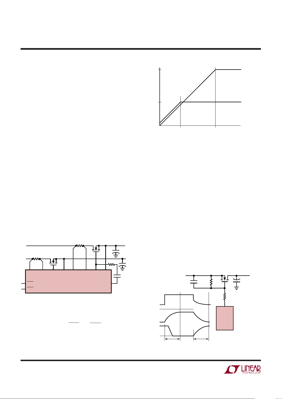
Figure 4. Supplies Turning On
12V
5V
1421 F4a
t
1
t
2
V
OUTHI
V
OUTLO
SLOPE = 20µA/C
RAMP
–12V
–12V
~1ms
0V
–12V
5V
CPON
9
B
R5
16k
5%
B
V
EE
0V
~1ms
1421 F05
R4
20k
5%
C2
0.047µF
C
LOAD
V
EE
–12V
1A
Q3
1/2 MMDF3N0HD
–12V FROM
CONNECTOR
+
CPON
LTC1421
Figure 5. Negative Supply Control
RAMP and GATEHI pins. The voltage at the GATEHI pin is
clamped one Schottky diode drop below GATELO.
The ramp time for each supply is equal to: t = (VCC)
(C
RAMP
)/20µA. During power down the gates are actively
pulled down by two internal NFETs.
A negative supply voltage can be controlled using the
CPON pin as shown in Figure 5.
When the board makes connection, the transistor Q3 is
turned off because it’s gate is pulled low to –12V by R4.
CPON is also pulled to –12V. When the charge pump is
turned on, CPON is pulled to V
CCLO
and the gate of Q3 will
ramp up with a time constant determined by R4, R5 and
C2. When the charge pump is turned off, CPON goes into
a high impedance state, the gate of Q3 is discharged to V
EE
with a time constant determined by R4 and C2, and Q3
turns off.
 Loading...