

Linear Technology LTC1417 Datasheet
FEATURES
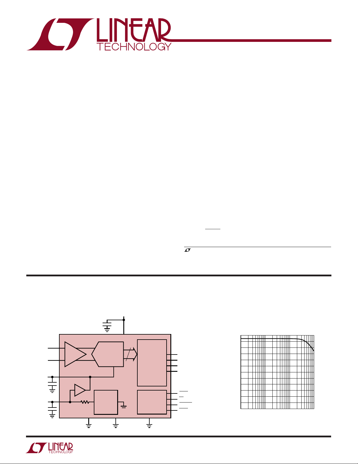
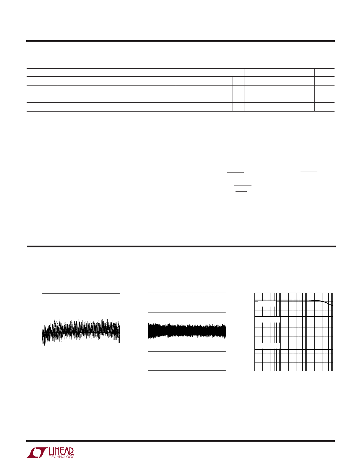
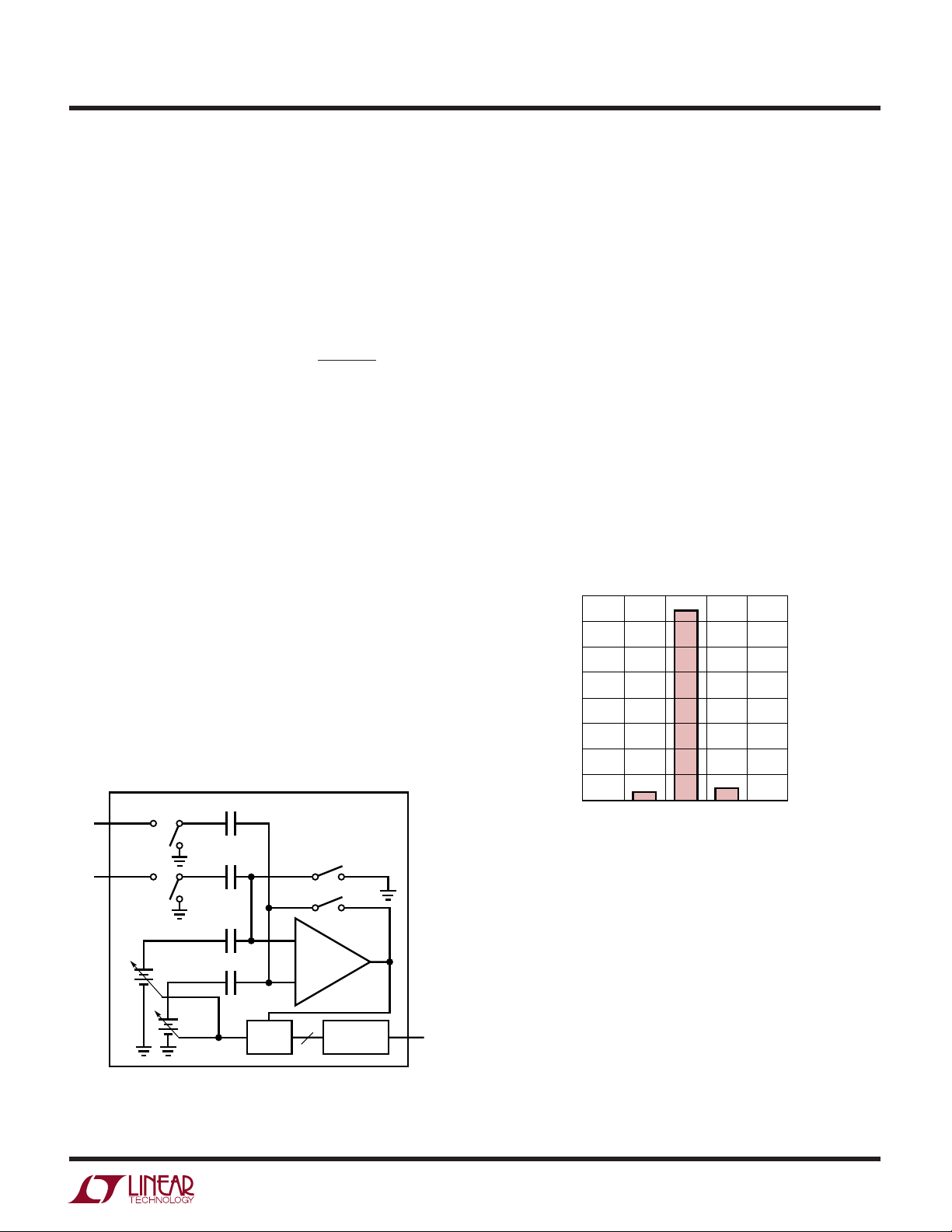
INPUT FREQUENCY (Hz)
4
EFFECTIVE BITS
S/(N + D) (dB)
6
8
10
12
10k 100k 1M
1417 TA02
2
1k
14 86
80
74
68
62
LTC1417
Low Power 14-Bit, 400ksps
Sampling ADC Converter
with Serial I/O
U
DESCRIPTIO
■
16-Pin Narrow SSOP Package (SO-8 Footprint)
■
Sample Rate: 400ksps
■
±1.25LSB INL and ±1LSB DNL Max
■
Power Dissipation: 20mW (Typ)
■
Single Supply 5V or ±5V Operation
■
Serial Data Output
■
No Missing Codes Over Temperature
■
Power Shutdown: Nap and Sleep
■
External or Internal Reference
■
Differential High Impedance Analog Input
■
Input Range: 0V to 4.096V or ±2.048V
■
81dB S/(N + D) and –95dB THD at Nyquist
U
APPLICATIO S
■
High Speed Data Acquisition
■
Digital Signal Processing
■
Isolated Data Acquisition Systems
■
Audio and Telecom Processing
■
Spectrum Instrumentation
The LTC®1417 is a low power, 400ksps, 14-bit A/D converter. This versatile device can operate from a single 5V or
±5V supplies. An onboard high performance sample-andhold, a precision reference and internal trimming minimize
external circuitry requirements. The low 20mW power
dissipation is made even more attractive with two userselectable power shutdown modes.
The LTC1417 converts 0V to 4.096V unipolar inputs when
using a 5V supply and ±2.048V bipolar inputs when using
±5V supplies. DC specs include ±1.25LSB INL, ±1LSB
DNL and no missing codes over temperature. Outstanding
AC performance includes 81dB S/(N + D) and 95dB THD
at a Nyquist input frequency of 200kHz.
The internal clock is trimmed for 2µs maximum conver-
sion time. A separate convert start input and a data ready
signal (BUSY) ease connections to FIFOs, DSPs and
microprocessors.
, LTC and LT are registered trademarks of Linear Technology Corporation.
U
EQUIVALE T BLOCK DIAGRA
A 400kHz, 14-Bit Sampling A/D Converter in a Narrow 16-Lead SSOP Package
LTC1417
1
+
A
IN
–
A
IN
REFCOMP
10µF
V
REF
1µF
S/H
2
4
BUFFER
3
4.096V
8k
REFERENCE
AGND
10µF
14-BIT ADC
2.5V
5V
VDD16
14
V
SS
(0V OR –5V)
SERIAL
PORT
TIMING AND
LOGIC
DGND10155
W
6
7
8
9
14
12
13
11
1417 TA01
EXTCLKIN
SCLK
CLKOUT
D
OUT
BUSY
RD
CONVST
SHDN
Effective Bits and Signal-to-(Noise + Distortion)
vs Input Frequency
1
LTC1417
O
A
S
(Notes 1, 2)
W
LUTEXI TIS
A
WUW
U
ARB
G
Positive Supply Voltage (VDD) .................................. 6V
Negative Supply Voltage (VSS)
Bipolar Operation Only .......................... –6V to GND
Total Supply Voltage (VDD to VSS)
Bipolar Operation Only ....................................... 12V
Analog Input Voltage (Note 3)
Unipolar Operation .................. – 0.3V to (VDD + 0.3V)
Bipolar Operation............ (VSS – 0.3) to (VDD + 0.3V)
Digital Input Voltage (Note 4)
Unipolar Operation ............................... –0.3V to 10V
Bipolar Operation.........................(VSS – 0.3V) to 10V
Digital Output Voltage
Unipolar Operation ................... –0.3 to (VDD + 0.3V)
Bipolar Operation........... (VSS – 0.3V) to (VDD + 0.3V)
Power Dissipation............................................. 500mW
Operating Temperature Range
LTC1417C .............................................. 0°C to 70°C
LTC1417I............................................ –40°C to 85°C
Storage Temperature Range ................ –65°C to 150°C
Lead Temperature (Soldering, 10 sec)................. 300°C
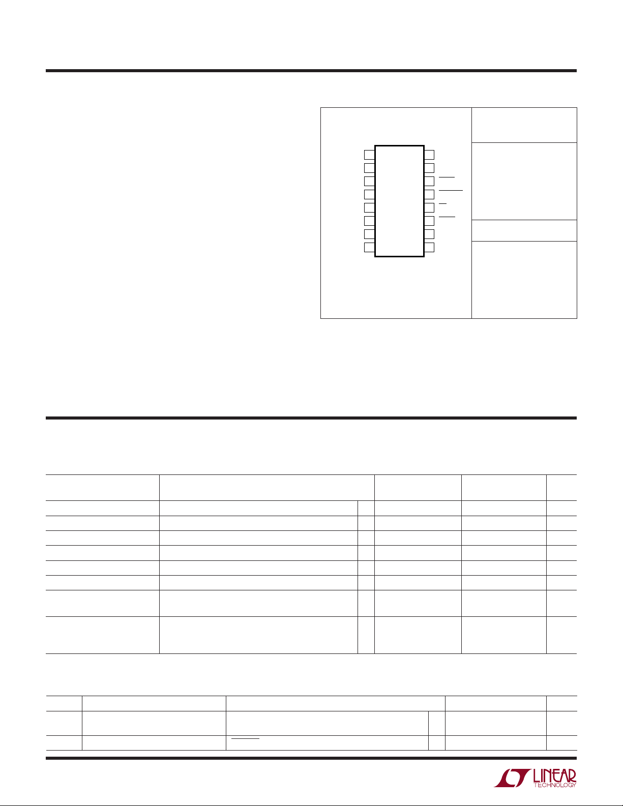
/
PACKAGE
+
1
A
IN
–
2
A
IN
3
V
REF
REFCOMP
EXTCLKIN
CLKOUT
Consult factory for Military grade parts.
4
5
AGND
6
7
SCLK
8
16-LEAD (NARROW) PLASTIC SSOP
T
JMAX
O
RDER I FOR ATIO
TOP VIEW
16
15
14
13
12
11
10
9
GN PACKAGE
= 110°C, θJA = 95°C/W
V
DD
V
SS
BUSY
CONVST
RD
SHDN
DGND
D
OUT
WU
ORDER
PART NUMBER
LTC1417ACGN
LTC1417CGN
LTC1417AIGN
LTC1417IGN
GN PART MARKING
1417A
1417
1417AI
1417I
U
U
CO
temperature range, otherwise specifications are at TA = 25°C. Specifications are measured while using the internal reference unless
otherwise noted. (Notes 5, 6)
PARAMETER CONDITIONS MIN TYP MAX MIN TYP MAX UNITS
Resolution ● 14 14 Bits
No Missing Codes ● 13 14 Bits
Integral Linearity Error (Note 7) ● ±0.8 ±2 ±0.5 ±1.25 LSB
Differential Linearity Error ● ±0.7 ±1.5 ±0.35 ±1 LSB
Transition Noise (Note 12) 0.33 0.33 LSB
Offset Error External Reference (Note 8) ● ±5 ±20 ±2 ±10 LSB
Full-Scale Error Internal Reference ±15 ±60 ±15 ±60 LSB
Full-Scale Tempco I
VERTER
CCHARA TERIST
External Reference = 2.5V ±5 ±30 ±5 ±15 LSB
= 0, Internal Reference, 0°C ≤ TA ≤ 70°C ±15 ±10 ppm/°C
OUT(REF)
= 0, Internal Reference, –40°C ≤ TA ≤ 85°C ±20 ppm/°C
I
OUT(REF)
I
= 0, External Reference ±5 ±1 ppm/°C
OUT(REF)
ICS
The ● indicates specifications which apply over the full operating
LTC1417 LTC1417A
RMS
UU
A ALOG I PUT
otherwise specifications are at TA = 25°C. (Note 5)
SYMBOL PARAMETER CONDITIONS MIN TYP MAX UNITS
V
IN
I
IN
Analog Input Range (Note 9) 4.75V ≤ VDD ≤ 5.25V (Unipolar) ● 0 to 4.096 V
Analog Input Leakage Current CONVST = High ● ±1 µA
The ● indicates specifications which apply over the full operating temperature range,
4.75V ≤ V
≤ 5.25V, –5.25V ≤ VSS ≤ –4.75V (Bipolar) ● ±2.048 V
DD
2
LTC1417
UU
A ALOG I PUT
otherwise specifications are at TA = 25°C. (Note 5)
SYMBOL PARAMETER CONDITIONS MIN TYP MAX UNITS
C
IN
t
ACQ
t
AP
t
jitter
CMRR Analog Input Common Mode Rejection Ratio 0V < (A
Analog Input Capacitance Between Conversions (Sample Mode) 14 pF
Sample-and-Hold Acquisition Time ● 150 500 ns
Sample-and-Hold Aperture Time –1.5 ns
Sample-and-Hold Aperture Time Jitter 5 ps
The ● indicates specifications which apply over the full operating temperature range,
During Conversions (Hold Mode) 3 pF
+
–
= A
IN
–2.048V < (A
) < 4.096V (Unipolar) 65 dB
IN
+
–
= A
IN
) < 2.048V (Bipolar) 65 dB
IN
RMS
UW
DY A IC ACCURACY
otherwise specifications are at TA = 25°C. (Note 5)
SYMBOL PARAMETER CONDITIONS MIN TYP MAX UNITS
S/(N + D) Signal-to-(Noise + Distortion) Ratio 100kHz Input Signal ● 79 81 dB
THD Total Harmonic Distortion 100kHz Input Signal, First Five Harmonics ● –85 –95 dB
SFDR Spurious Free Dynamic Range 200kHz Input Signal –98 dB
IMD Intermodulation Distortion f
Full Power Bandwidth 10 MHz
Full Linear Bandwidth S/(N + D) ≥ 77dB 0.8 MHz
The ● indicates specifications which apply over the full operating temperature range,
= 97.3kHz, f
IN1
= 104.6kHz –97 dB
IN2
UU U
I TER AL REFERE CE CHARACTERISTICS
operating temperature range, otherwise specifications are at TA = 25°C. (Note 5)
The ● indicates specifications which apply over the full
PARAMETER CONDITIONS MIN TYP MAX UNITS
V
Output Voltage I
REF
V
Output Tempco I
REF
V
Line Regulation 4.75V ≤ VDD ≤ 5.25V 0.05 LSB/V
REF
V
Output Resistance 0.1mA ≤ |I
REF
= 0 ● 2.480 2.500 2.520 V
OUT
= 0, 0°C ≤ TA ≤ 70°C ±10 ppm/°C
OUT
= 0, –40°C ≤ TA ≤ 85°C ±20 ppm/°C
I
OUT
–5.25V ≤ V
≤ –4.75V 0.05 LSB/V
SS
| ≤ 0.1mA 8 kΩ
OUT
UU
DIGITAL I PUTS A D DIGITAL OUTPUTS
operating temperature range, otherwise specifications are at TA = 25°C. (Note 5)
SYMBOL PARAMETER CONDITIONS MIN TYP MAX UNITS
V
IH
V
IL
I
IN
C
IN
V
OH
V
OL
I
OZ
C
OZ
I
SOURCE
I
SINK
High Level Input Voltage V
Low Level Input Voltage VDD = 4.75V ● 0.8 V
Digital Input Current VIN = 0V to V
Digital Input Capacitance 1.4 pF
High Level Output Voltage VDD = 4.75V, IO = –10µA 4.74 V
Low Level Output Voltage VDD = 4.75V, IO = 160µA 0.05 V
High-Z Output Leakage D
High-Z Output Capacitance D
Output Source Current V
Output Sink Current V
, CLKOUT V
OUT
, CLKOUT RD High (Note 9) ● 15 pF
OUT
= 5.25V ● 2.4 V
DD
DD
VDD = 4.75V, IO = –200µA ● 4.0 V
VDD = 4.75V, IO = –1.6mA ● 0.10 0.4 V
= 0V to VDD, RD High ● ±10 µA
OUT
= 0V –10 mA
OUT
= V
OUT
DD
The ● indicates specifications which apply over the full
● ±10 µA
10 mA
3
LTC1417
WU
POWER REQUIRE E TS
otherwise specifications are at TA = 25°C. (Note 5)
SYMBOL PARAMETER CONDITIONS MIN TYP MAX UNITS
V
DD
V
SS
I
DD
I
SS
P
DIS
Positive Supply Voltage (Notes 10, 11) 4.75 5.25 V
Negative Supply Voltage (Note 10) Bipolar Only (VSS = 0V for Unipolar) – 4.75 –5.25 V
Positive Supply Current Unipolar, RD High (Note 5) ● 4.0 5.5 mA
Nap Mode SHDN = 0V, RD = 0V 750 µA
Sleep Mode SHDN = 0V, RD = 5V 0.1 µA
Negative Supply Current Bipolar, RD High (Note 5) ● 2.0 2.8 mA
Nap Mode SHDN = 0V, RD = 0V 0.7 µA
Sleep Mode SHDN = 0V, RD = 5V 1.5 nA
Power Dissipation Unipolar ● 20.0 27.5 mW
The ● indicates specifications which apply over the full operating temperature range,
Bipolar, RD High (Note 5)
Bipolar
● 4.3 6.0 mA
● 31.5 44 mW
UW
TI I G CHARACTERISTICS
range, otherwise specifications are at TA = 25°C. (Note 5)
SYMBOL PARAMETER CONDITIONS MIN TYP MAX UNITS
f
SAMPLE(MAX)
t
CONV
t
ACQ
t
+ t
ACQ
CONV
t
1
t
2
t
3
t
4
t
5
t
6
t
7
t
8
t
9
t
10
t
11
t
12
f
SCLK
f
EXTCLKIN
t
dEXTCLKIN
Maximum Sampling Frequency ● 400 kHz
Conversion Time ● 1.8 2.25 µs
Acquisition Time ● 150 500 ns
Acquisition Plus Conversion Time ● 2.1 2.5 µs
SHDN↑ to CONVST↓ Wake-Up Time from Nap Mode (Note 10) 500 ns
CONVST Low Time (Notes 10, 11) ● 40 ns
CONVST to BUSY Delay CL = 25pF ● 35 70 ns
Data Ready Before BUSY↑ CL = 25pF ● 712 ns
Delay Between Conversions (Note 10) ● 250 ns
Wait Time RD↓ After BUSY↑ ● –5 ns
Data Access Time After RD↓ CL = 25pF 15 30 ns
Bus Relinquish Time ● 35 ns
RD Low Time ● t
CONVST High Time ● 40 ns
Delay Time, SCLK↓ to D
Time from Previous Data Remain Valid After SCLK↓ CL = 25pF ● 510 ns
Shift Clock Frequency (Note 13) ● 0 20 MHz
External Conversion Clock Frequency ● 0.05 9 MHz
Delay Time, CONVST↓ to External Conversion Clock Input (Note 9) ● 20 µs
Valid CL = 25pF ● 15 40 ns
OUT
The ● indicates specifications which apply over the full operating temperature
● 40 ns
CL = 100pF 20 40 ns
● 55 ns
7
ns
4
LTC1417
UW
TI I G CHARACTERISTICS
range, otherwise specifications are at TA = 25°C. (Note 5)
SYMBOL PARAMETER CONDITIONS MIN TYP MAX UNITS
t
H SCLK
t
L SCLK
t
H EXTCLKIN
t
L EXTCLKIN
SCLK High Time (Note 9) ● 10 ns
SCLK Low Time (Note 9) ● 10 ns
EXTCLKIN High Time ● 0.04 20 µs
EXTCLKIN Low Time ● 0.04 20 µs
The ● indicates specifications which apply over the full operating temperature
Note 1: Absolute Maximum Ratings are those values beyond which the life
of a device may be impaired.
Note 2: All voltage values are with respect to ground with DGND and
AGND wired together (unless otherwise noted).
Note 3: When these pin voltages are taken below V
or above VDD, they
SS
will be clamped by internal diodes. This product can handle input currents
greater than 100mA without latchup if the pin is driven below VSS (ground
for unipolar mode) or above VDD.
Note 4: When these pin voltages are taken below V
they will be clamped
SS
by internal diodes. This product can handle input currents greater than
100mA below VSS without latchup. These pins are not clamped to VDD.
Note 5: V
= 5V, VSS = –5V, f
DD
= 400kHz, tr = tf = 5ns unless
SAMPLE
otherwise specified.
Note 6: Linearity, offset and full-scale specifications apply for a single-
ended A
+
input with A
IN
–
grounded.
IN
Note 7: Integral nonlinearity is defined as the deviation of a code from a
straight line passing through the actual endpoints of the transfer curve.
The deviation is measured from the center of the quantization band.
Note 8: Bipolar offset is the offset voltage measured from –0.5LSB
when the output code flickers between 0000 0000 0000 00 and
1111 1111 1111 11.
Note 9: Guaranteed by design, not subject to test.
Note 10: Recommended operating conditions.
Note 11: The falling CONVST edge starts a conversion. If CONVST returns
high at a critical point during the conversion it can create small errors. For
best results ensure that CONVST returns high either within 625ns after
conversion start or after BUSY rises.
Note 12: Typical RMS noise at the code transitions. See Figure 2 for
histogram.
Note 13: t
of 40ns maximum allows f
11
capture with 50% duty cycle. f
5ns setup time.
UW
TYPICAL PERFOR A CE CHARACTERISTICS
Differential Nonlinearity
Typical INL Curve
1.0
0.5
0
INL (LSBs)
–0.5
–1.0
40960
8192
OUTPUT CODE
12288 16384
1417 G01
vs Output Code
1.0
0.5
0
DNL ERROR (LSBs)
–0.5
–1.0
0
4096 8192
OUTPUT CODE
12288 16384
(TA = 25°C)
1417 G02
up to 10MHz for rising
SCLK
up to 20MHz for falling capture with
SCLK
S/(N + D) vs Input Frequency
and Amplitude
90
80
VIN = 0dB
70
60
VIN = –20dB
50
40
30
VIN = –60dB
20
SIGNAL/(NOISE + DISTORTION) (dB)
10
0
1k 100k 1M
10k
INPUT FREQUENCY (Hz)
1417 G03
5
LTC1417
FREQUENCY (kHz)
0
–120
AMPLITUDE (dB)
–100
–80
–60
–40
40 100
140
200
1417 G09
–20
0
20 60 80
120
160 180
f
SAMPLE
= 400kHz
f
IN1
= 97.303466kHz
f
IN2
= 104.632568kHz
V
IN
= 4.096V
P-P
UW
TYPICAL PERFOR A CE CHARACTERISTICS
(TA = 25°C)
Signal-to-Noise Ratio
vs Input Frequency Distortion vs Input Frequency
90
80
70
60
50
40
30
20
SIGNAL-TO-NOISE RATIO (dB)
10
0
1k
INPUT FREQUENCY (Hz)
Nonaveraged, 4096 Point FFT,
Input Frequency = 10kHz
0
–20
–40
f
SAMPLE
= 10.05859375kHz
f
IN
SFDR = –97.44dB
SINAD = 81.71dB
100k 1M10k
1417 G04
= 400kHz
0
–20
–40
–60
–80
–100
AMPLITUDE (dB BELOW THE FUNDAMENTAL)
–120
1
10 100
INPUT FREQUENCY (kHz)
THD
2ND
Nonaveraged, 4096 Point FFT,
Input Frequency = 200kHz Intermodulation Distortion Plot
0
f
= 400kHz
SAMPLE
= 197.949188kHz
f
IN
SFDR = –98dB
–20
SINAD = 81.1dB
–40
3RD
1417 G05
1000
Spurious-Free Dynamic Range
vs Input Frequency
0
–20
–40
–60
–80
–100
SPURIOUS FREE DYNAMIC RANGE (dB)
–120
1k
10k 100k 1M
INPUT FREQUENCY (Hz)
1417 G06
–60
AMPLITUDE (dB)
–80
–100
–120
0 10050
FREQUENCY (kHz)
Power Supply Feedthrough
vs Ripple Frequency
0
V
= 60mV
RIPPLE
= 400kHz
f
SAMPLE
20
= 200kHz
f
IN
40
60
80
FEEDTHROUGH (dB)
100
120
1k
10k 100k
RIPPLE FREQUENCY (Hz)
V
–60
AMPLITUDE (dB)
–80
–100
150
SS
V
DGND
1M 10M
200
1417 G07
DD
1417 G10
–120
0 50 100
FREQUENCY (kHz)
Input Common Mode Rejection
vs Input Frequency
70
60
50
40
30
20
COMMON MODE REJECTION (dB)
10
0
1
10
INPUT FREQUENCY (kHz)
150
100 1000
200
1417 G08
1417 G11
Input Offset Voltage Shift
vs Source Resistance
10
9
8
7
6
5
4
3
2
CHANGE IN OFFSET VOTLAGE (LSB)
1
0
110
100 1k 10k 100k 1M
INPUT SOURCE RESISTANCE (Ω)
1417 G12
6
UW
TYPICAL PERFOR A CE CHARACTERISTICS
LTC1417
(TA = 25°C)
VDD Supply Current vs
Temperature (Unipolar Mode)
6
5
4
3
2
SUPPLY CURRENT (mA)
DD
V
1
0
–50 150
–75
0 25 50 100
–25
TEMPERATURE (°C)
VDD Supply Current vs Sampling
Frequency (Unipolar Mode)
5.0
4.5
4.0
3.5
3.0
2.5
2.0
1.5
SUPPLY CURRENT (mA)
DD
V
1.0
0.5
0
100
050
SAMPLING FREQUENCY (kHz)
300 350
200150
250
VDD Supply Current vs
Temperature (Bipolar Mode)
6
5
4
3
2
SUPPLY CURRENT (mA)
DD
V
1
125
75
1417 G13
0
–50 150
–75
0 25 50 100
–25
TEMPERATURE (°C)
75
125
1417 G14
VDD Supply Current vs Sampling
Frequency (Bipolar Mode)
5.0
4.5
4.0
3.5
3.0
2.5
2.0
1.5
SUPPLY CURRENT (mA)
DD
V
1.0
0.5
0
400 450
1417 G16
500
100
050
SAMPLING FREQUENCY (kHz)
300 350
400 450
200150
250
500
1417 G17
VSS Supply Current vs
Temperature (Bipolar Mode)
3.0
2.5
2.0
1.5
1.0
SUPPLY CURRENT (mA)
SS
V
0.5
0
–50 150
–75
0 25 50 100
–25
TEMPERATURE (°C)
VSS Supply Current vs Sampling
Frequency (Bipolar Mode)
2.5
2.0
1.5
1.0
SUPPLY CURRENT (mA)
SS
V
0.5
0
100
050
SAMPLING FREQUENCY (kHz)
300 350
200150
250
125
75
1417 G15
400 450
500
1417 G18
UUU
PIN FUNCTIONS
+
A
(Pin 1): Positive Analog Input.
IN
–
A
(Pin 2): Negative Analog Input.
IN
V
(Pin 3): 2.50V Reference Output. Bypass to AGND
REF
with 1µF.
REFCOMP (Pin 4): 4.096V Reference Output. Bypass to
AGND using 10µF tantalum in parallel with 0.1µF ceramic.
AGND (Pin 5): Analog Ground.
EXTCLKIN (Pin 6): External Conversion Clock Input. A 5V
input will enable the internal conversion clock.
SCLK (Pin 7): Data Clock Input.
CLKOUT (Pin 8): Conversion Clock Output.
D
(Pin 9): Serial Data Output.
OUT
DGND (Pin 10): Digital Ground.
SHDN (Pin 11): Power Shutdown Input. Low selects
shutdown. Shutdown mode selected by RD. RD = 0V for
Nap mode and RD = 5V for Sleep mode.
RD (Pin 12): Read Input. This enables the output drivers.
RD also sets the shutdown mode when SHDN goes low.
RD and SHDN low selects the quick wake-up Nap mode,
RD high and SHDN low selects Sleep mode.
7
LTC1417
UUU
PIN FUNCTIONS
CONVST (Pin 13): Conversion Start Signal. This active
low signal starts a conversion on its falling edge.
BUSY (Pin 14): The BUSY output shows the converter
status. It is low when a conversion is in progress.
TEST CIRCUITS
Load Circuits for Access Timing Load Circuits for Output Float Delay
5V
1k
D
OUT
A) HI-Z TO V
1k C
DGND
AND VOL TO V
OH
L
OH
D
OUT
B) HI-Z TO V
C
L
DGND
AND VOH TO V
OL
OL
1417 TC01
VSS (Pin 15): Negative Supply, –5V for Bipolar Operation.
Bypass to AGND using 10µF tantalum in parallel with
0.1µF ceramic. Analog ground for unipolar operation.
VDD (Pin 16): 5V Positive Supply. Bypass to AGND with
10µF tantalum in parallel with 0.1µF ceramic.
5V
1k
D
OUT
1k
A) VOH TO HI-Z
30pF
D
OUT
30pF
TO HI-Z
B) V
OL
1417 TC02
UU
W
FUNCTIONAL BLOCK DIAGRA
C
SAMPLE
C
SAMPLE
14-BIT CAPACITIVE DAC
SUCCESSIVE APPROXIMATION
CONTROL LOGIC
CONVST RD CLKOUTSHDN
A
IN
A
IN
V
REF
REFCOMP
(4.096V)
AGND
DGND
1
+
2
–
8k
3
4
5
10
INTERNAL
CLOCK
2.5V REF
MUX
EXTCLKIN
REGISTER
ZEROING SWITCHES
+
COMPREF AMP
–
14
SHIFT REGISTER
1481213116
BUSY
16
V
DD
V
SS
15
(0V FOR UNIPOLAR MODE
–5V FOR BIPOLAR MODE)
9
D
OUT
7
SCLK
1417 BD
8
LTC1417
U
WUU
APPLICATIONS INFORMATION
CONVERSION DETAILS
The LTC1417 uses a successive approximation algorithm
and an internal sample-and-hold circuit to convert an
analog signal to a 14-bit serial output. The ADC is complete with a precision reference and an internal clock. The
control logic provides easy interface to microprocessors
and DSPs (please refer to Digital Interface section for the
data format).
Conversion start is controlled by the CONVST input. At the
start of the conversion, the successive approximation
register (SAR) is reset. Once a conversion cycle has
begun, it cannot be restarted.
During the conversion, the internal differential 14-bit
capacitive DAC output is sequenced by the SAR from the
most significant bit (MSB) to the least significant bit (LSB).
Referring to Figure 1, the A
nected to the sample-and-hold capacitors (C
ing the acquire phase and the comparator offset is nulled by
the zeroing switches. In this acquire phase, a minimum
delay of 500ns will provide enough time for the sampleand-hold capacitors to acquire the analog signal. During
the convert phase, the comparator zeroing switches open,
placing the comparator in compare mode. The input
switches connect the C
transferring the differential analog input charge onto the
C
HOLD
HOLD
+
V
DAC
C
–
SAMPLE
SAMPLE
C
DAC
C
DAC
SAMPLE
+
A
IN
SAMPLE
–
A
IN
V
DAC
Figure 1. Simplified Block Diagram
IN
SAMPLE
+
–
+
–
SAR
+
and A
–
inputs are con-
IN
SAMPLE
capacitors to ground,
ZEROING SWITCHES
HOLD
HOLD
+
COMP
–
14
SHIFT
REGISTER
1417 F01
) dur-
D
OUT
summing junction. This input charge is successively
compared with the binary weighted charges supplied by
the differential capacitive DAC. Bit decisions are made by
the high speed comparator. At the end of a conversion, the
differential DAC output balances the A
IN
+
and A
IN
–
input
charges. The SAR contents (a 14-bit data word) that
represent the difference of A
through the serial pin D
OUT
.
IN
+
and A
–
are output
IN
DC Performance
One way of measuring the transition noise associated with
a high resolution ADC is to use a technique where a DC
signal is applied to the input of the ADC and the resulting
output codes are collected over a large number of conversions. For example in Figure 2, the distribution of output
code is shown for a DC input that has been digitized 4096
times. The distribution is Gaussian and the RMS code
transition is about 0.33LSB.
4000
3500
3000
2500
2000
COUNTS
1500
1000
500
0
–1 0 2
–2
CODE
1
1417 F02
Figure 2. Histogram for 4096 Conversions
DYNAMIC PERFORMANCE
The LTC1417 has excellent high speed sampling capability. FFT (Fast Fourier Transform) test techniques are used
to test the ADC’s frequency response, distortion and
noise performance at the rated throughput. By applying
a low distortion sine wave and analyzing the digital output
using an FFT algorithm, the ADC’s spectral content can be
examined for frequencies beyond the fundamental.
Figure 3 shows a typical LTC1417 FFT plot.
9
LTC1417
U
WUU
APPLICATIONS INFORMATION
0
–20
–40
–60
AMPLITUDE (dB)
–80
–100
–120
0 10050
Figure 3a. LTC1417 Nonaveraged, 4096 Point FFT,
Input Frequency = 10kHz
0
f
= 400kHz
SAMPLE
= 197.949188kHz
f
IN
SFDR = –98dB
–20
SINAD = 81.1dB
–40
f
SAMPLE
= 10.05859375kHz
f
IN
SFDR = –97.44dB
SINAD = 81.71dB
FREQUENCY (kHz)
= 400kHz
150
200
1417 G07
Effective Number of Bits
The effective number of bits (ENOBs) is a measurement of
the resolution of an ADC and is directly related to the
S/(N + D) by the equation:
ENOB (N) = [S/(N + D) – 1.76]/6.02
where N is the effective number of bits of resolution and
S/(N + D) is expressed in dB. At the maximum sampling
rate of 400kHz, the LTC1417 maintains near ideal ENOBs
up to the Nyquist input frequency of 200kHz (refer to
Figure 4).
14 86
80
12
10
8
EFFECTIVE BITS
6
74
68
S/(N + D) (dB)
62
–60
AMPLITUDE (dB)
–80
–100
–120
0 50 100
FREQUENCY (kHz)
150
200
1417 G08
Figure 3b. LTC1417 Nonaveraged, 4096 Point FFT,
Input Frequency = 200kHz
Signal-to-Noise Ratio
The signal-to-noise plus distortion ratio [S/(N + D)] is the
ratio between the RMS amplitude of the fundamental input
frequency to the RMS amplitude of all other frequency
components at the A/D output. The output is band limited
to frequencies from above DC and below half the sampling
frequency. Figure 3b shows a typical spectral content with
a 400kHz sampling rate and a 200kHz input. The dynamic
performance is excellent for input frequencies up to and
beyond the Nyquist limit of 200kHz.
4
2
1k
10k 100k 1M
INPUT FREQUENCY (Hz)
1417 TA02
Figure 4. Effective Bits and Signal/(Noise + Distortion)
vs Input Frequency
Total Harmonic Distortion
Total harmonic distortion (THD) is the ratio of the RMS
sum of all harmonics of the input signal to the fundamental
itself. The out-of-band harmonics alias into the frequency
band between DC and half the sampling frequency. THD is
expressed as:
222 2
VVV Vn
+++
THD Log
=
20
234
V
1
...
where V1 is the RMS amplitude of the fundamental frequency and V2 through Vn are the amplitudes of the
second through nth harmonics. THD vs Input Frequency is
shown in Figure 5. The LTC1417 has good distortion
performance up to the Nyquist frequency and beyond.
10
 Loading...