

Linear Technology LTC1414 Datasheet
INPUT FREQUENCY (Hz)
EFFECTIVE BITS
S/(N + D) (dB)
10k 100k 1M 10M
1414 TA02
1k
14
13
12
11
10
9
8
7
6
5
4
3
2
86
80
74
68
f
SAMPLE
= 2.2MHz
FEATURES
LTC1414
14-Bit, 2.2Msps,
Sampling A/D Converter
U
DESCRIPTIO
■
Sample Rate: 2.2Msps
■
Outstanding Spectral Purity:
80dB S/(N + D) and 95dB SFDR at 100kHz
78dB S/(N + D) and 84dB SFDR at Nyquist
■
Ultralow Distortion with Single-Ended or
Differential Inputs
■
±2.5V Bipolar Input Range Eliminates Level Shifting
and Rail-to-Rail Op Amp Requirements
■
Easy Hookup for External or Internal Reference
■
No Pipeline Delay
■
Power Dissipation: 175mW on ±5V Supplies
■
28-Pin Narrow SSOP Package
U
APPLICATIO S
■
Telecommunications
■
Digital Signal Processing
■
Multiplexed Data Acquisition Systems
■
High Speed Data Acquisition
■
Spectrum Analysis
■
Imaging Systems
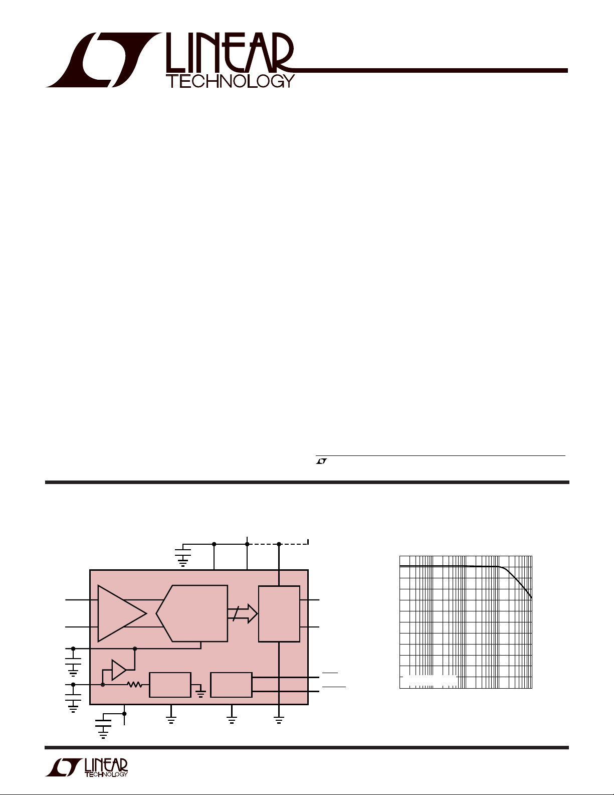
The LTC®1414 is a 14-bit, 2.2Msps, sampling A/D converter which draws only 175mW from ±5V supplies. This
high performance ADC includes a high dynamic range
sample-and-hold, a precision reference and requires no
external components.
The LTC1414’s high performance sample-and-hold has a
full-scale input range of ± 2.5V. Outstanding AC performance includes 80dB S/(N + D) and 95dB SFDR with a
100kHz input. The performance remains high at the Nyquist
input frequency of 1.1MHz with 78dB S/(N + D) and 84dB
SFDR.
The unique differential input sample-and-hold can acquire
single-ended or differential input signals up to its 40MHz
bandwidth. The 70dB common mode rejection can eliminate ground loops and common mode noise by measuring
signal differentially from the source
The ADC has a microprocessor compatible, 14-bit parallel
output port. There is no pipline delay in the conversion
results.
, LTC and LT are registered trademarks of Linear Technology Corporation.
TYPICAL APPLICATIO
COMP
LTC1414
+
A
IN
S/H
–
A
IN
4.0625V
10µF
V
REF
1µF
10µF
BUFFER
–5V
2k
V
SS
14-BIT ADC
2.5V
REFERENCE
AGND
10µF
U
AV
DD
TIMING AND
LOGIC
5V
14
DGND
DV
DD
OUTPUT
BUFFERS
OPTIONAL 3V
LOGIC SUPPLY
OV
DD
•
•
•
OGND
Effective Bits and Signal-to-Noise + Distortion
vs Input Frequency
D13 (MSB)
D0 (LSB)
BUSY
CONVST
1414 TA01
1

LTC1414
WW
W
U
ABSOLUTE MAXIMUM RATINGS
AVDD = OVDD = DVDD = V
Supply Voltage (VDD)................................................. 6V
Negative Supply Voltage (VSS) ................................–6V
Total Supply Voltage (VDD to VSS) .......................... 12V
Analog Input Voltage
(Note 3).........................(VSS – 0.3V) to (VDD + 0.3V)
Digital Input Voltage (Note 4) ..........(VSS – 0.3V) to 10V
Digital Output Voltage........(VSS – 0.3V) to (VDD + 0.3V)
Power Dissipation.............................................. 500mW
Operating Temperature Range.....................0°C to 70°C
Storage Temperature Range................. –65°C to 150°C
Lead Temperature (Soldering, 10 sec)..................300°C
(Notes 1, 2)
DD
W
PACKAGE/ORDER INFORMATION
TOP VIEW
+
1
A
IN
–
2
A
IN
3
V
REF
REFCOMP
D13 (MSB)
Consult factory for Industrial, Military and A grade parts.
4
5
AGND
6
7
D12
8
D11
9
D10
10
D9
11
D8
12
D7
13
D6
14
OGND
GN PACKAGE
28-LEAD PLASTIC SSOP
T
= 110°C, θJA = 110°C/W
JMAX
28
27
26
25
24
23
22
21
20
19
18
17
16
15
AV
DD
AGND
V
SS
BUSY
CONVST
DGND
DV
DD
OV
DD
D0
D1
D2
D3
D4
D5
ORDER PART
NUMBER
LTC1414CGN
UU
U
With internal reference (Notes 5, 6)
–
+
= A
IN
) < 2.5V 70 dB
IN
LTC1414
● ±24 LSB
RMS
U
IN
IN
VERTER
CCHARA TERIST
External Reference = 2.5V ±5 ±25 LSB
External Reference = 2.5V ±1 ppm/°C
ICS
U
PUT
LOG
Analog Input Range 4.75V ≤ VDD ≤ 5.25V, –5.25V ≤ VSS ≤ –4.75V ● ±2.5 V
Analog Input Leakage Current Between Conversions ● ±1 µA
Analog Input Capacitance Between Conversions 8 pF
Sample-and-Hold Acquisition Time ● 40 100 ns
Sample-and-Hold Aperture Delay Time –1 ns
Sample-and-Hold Aperture Delay Time Jitter 3 ps
IA
(Note 5)
During Conversions 4 pF
CO
PARAMETER CONDITIONS MIN TYP MAX UNITS
Resolution (No Missing Codes) ● 13 Bits
Integral Linearity Error (Note 7) ● ±0.75 ±2.0 LSB
Differential Linearity Error ● ±0.75 ±1.75 LSB
Offset Error (Note 8) ±5 ±20 LSB
Full-Scale Error Internal Reference ±10 ±60 LSB
Full-Scale Tempco Internal Reference ±15 ppm/°C
A
SYMBOL PARAMETER CONDITIONS MIN TYP MAX UNITS
V
I
IN
C
t
ACQ
t
AP
t
jitter
CMRR Analog Input Common Mode Rejection Ratio –2.5V < (A
2
LTC1414
W
U
IC
DY
SYMBOL PARAMETER CONDITIONS MIN TYP MAX UNITS
S/(N + D) Signal-to-Noise Plus Distortion Ratio 100kHz Input Signal 80 dB
THD Total Harmonic Distortion 100kHz Input Signal, First 5 Harmonics –95 dB
SFDR Spurious Free Dynamic Range 100kHz Input Signal, First 5 Harmonics 95 dB
IMD Intermodulation Distortion f
A
Full Power Bandwidth 40 MHz
Full Linear Bandwidth S/(N + D) ≥ 74dB 3 MHz
ACCURAC Y
(Note 5)
1.1MHz Input Signal 78 dB
1.1MHz Input Signal, First 5 Harmonics –83 dB
1.1MHz Input Signal, First 5 Harmonics 84 dB
= 29.37kHz, f
IN1
= 32.446kHz –86 dB
IN2
U
I TER AL REFERE CE CHARACTERISTICS
PARAMETER CONDITIONS MIN TYP MAX UNITS
V
REF
V
REF
V
REF
V
REF
COMP Output Voltage I
UU
(Note 5)
Output Voltage I
Output Tempco I
Line Regulation 4.75V ≤ VDD ≤ 5.25V 0.01 LSB/V
Output Resistance I
= 0 2.480 2.500 2.520 V
OUT
= 0 ±15 ppm/°C
OUT
–5.25V ≤ V
OUT
= 0 4.06 V
OUT
≤ –4.75V 0.01 LSB/V
SS
≤ 0.1mA 2 kΩ
UU
DIGITAL I PUTS AND OUTPUTS
SYMBOL PARAMETER CONDITIONS MIN TYP MAX UNITS
V
IH
V
IL
I
IN
C
IN
V
OH
V
OL
I
SOURCE
I
SINK
High Level Input Voltage V
Low Level Input Voltage VDD = 4.75V ● 0.8 V
Digital Input Current VIN = 0V to V
Digital Input Capacitance 1.2 pF
High Level Output Voltage VDD = 4.75V, IO = –10µA 4.74 V
Low Level Output Voltage VDD = 4.75V, IO = 160µA 0.05 V
Output Source Current V
Output Sink Current V
(Note 5)
= 5.25V ● 2.4 V
DD
DD
VDD = 4.75V, IO = –200µA ● 4.0 V
VDD = 4.75V, IO = 1.6mA ● 0.10 0.4 V
= 0V –10 mA
OUT
= V
OUT
DD
● ±10 µA
10 mA
U
W
POWER REQUIRE E TS
SYMBOL PARAMETER CONDITIONS MIN TYP MAX UNITS
V
DD
V
SS
I
DD
I
SS
P
D
Positive Supply Voltage (Note 9) 4.75 5.25 V
Negative Supply Voltage (Note 9) –4.75 –5.25 V
Positive Supply Current CS High ● 12 16 mA
Negative Supply Current CS High ● 23 30 mA
Power Dissipation 175 230 mW
(Note 5)
3
LTC1414
INPUT FREQUENCY (Hz)
10k
DISTORTION (dB)
0
–10
–20
–30
–40
–50
–60
–70
–80
–90
–100
100k 1M 10M
1414 G03
2nd
THD
3rd
W
U
TI I G CHARACTERISTICS
SYMBOL PARAMETER CONDITIONS MIN TYP MAX UNITS
f
SAMPLE(MAX)
t
CONV
t
ACQ
t
THROUGHPUT
t
1
t
2
t
3
t
4
t
5
t
6
The ● denotes specifications which apply over the full operating
temperature range; all other limits and typicals TA = 25°C.
Note 1: Absolute Maximum Ratings are those values beyond which the life
of a device may be impaired.
Note 2: All voltage values are with respect to ground with DGND and
AGND wired together (unless otherwise noted).
Note 3: When these pin voltages are taken below V
will be clamped by internal diodes. This product can handle input currents
greater than 100mA below VSS or above VDD without latchup.
Note 4: When these pin voltages are taken below V
by internal diodes. This product can handle input currents greater than
100mA below VSS without latchup. These pins are not clamped to VDD.
Note 5: V
otherwise specified.
Maximum Sampling Frequency ● 2.2 MHz
Conversion Time ● 220 330 400 ns
Acquisition Time ● 40 100 ns
Throughput Time (Acquisition + Conversion) ● 370 454 ns
CONVST to BUSY Delay CL = 25pF 10 ns
Data Ready Before BUSY↑ ±20 ns
Delay Between Conversions (Note 9) ● 100 ns
CONVST Low Time (Note 10) ● 40 ns
CONVST High Time (Note 10) ● 40 ns
Aperture Delay of Sample-and-Hold –1 ns
SS
SS
= 5V, VSS = –5V, f
DD
= 2.2MHz and tr = tf = 5ns unless
SAMPLE
(Note 5)
or above VDD, they
, they will be clamped
Note 6: Linearity, offset and full-scale specifications apply for a singleended A
+
input with A
IN
–
grounded.
IN
Note 7: Integral nonlinearity is defined as the deviation of a code from a
straight line passing through the actual endpoints of the transfer curve.
The deviation is measured from the center of the quantization band.
Note 8: Bipolar offset is the offset voltage measured from –0.5LSB
when the output code flickers between 0000 0000 0000 00 and
1111 1111 1111 11.
Note 9: Recommended operating conditions.
Note 10: The falling CONVST edge starts a conversion. If CONVST returns
high at a critical point during the conversion it can create small errors. For
best results ensure that CONVST returns high either within 225ns after the
start of the conversion or after BUSY rises.
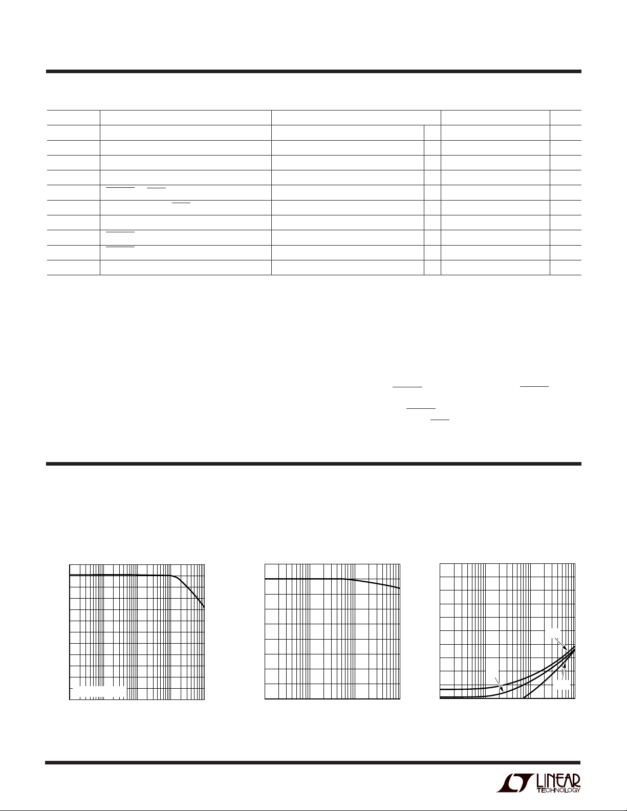
TYPICAL PERFOR A CE CHARACTERISTICS
4
UW
Signal-to-Noise Ratio vs Input
S/(N + D) vs Input Frequency Distortion vs Input Frequency
14
13
12
11
10
9
8
7
EFFECTIVE BITS
6
5
4
3
f
= 2.2MHz
SAMPLE
2
1k
10k 100k 1M 10M
INPUT FREQUENCY (Hz)
86
80
74
68
S/(N + D) (dB)
1414 TA02
Frequency
90
80
70
60
50
40
30
20
SIGNAL-TO-NOISE RATIO (dB)
10
0
10k
100k 1M 10M
INPUT FREQUENCY (Hz)
1414 G02

UW
OUTPUT CODE
0 4096 8192 12288 16384
DNL (LSBs)
1414 G06
2.0
1.0
0
–1.0
–2.0
TYPICAL PERFOR A CE CHARACTERISTICS
LTC1414
Spurious-Free Dynamic Range vs
Input Frequency Intermodulation Distortion Plot
0
–10
–20
–30
–40
–50
–60
–70
–80
–90
SPURIOUS-FREE DYNAMIC RANGE (dB)
–100
10k
100k 1M 10M
INPUT FREQUENCY (Hz)
Integral Nonlinearity vs Output
Code
2.0
1.0
0
INL (LSBs)
–1.0
–2.0
0 4096 8192 12288 16384
OUTPUT CODE
1414 G04
1414 G07
0
–20
–40
–60
AMPLITUDE (dB)
–80
–100
–120
0
FREQUENCY (kHz)
f
SAMPLE
f
IN1
f
IN2
400 800200 600 1000
Power Supply Feedthrough vs
Ripple Frequency
0
–20
–40
–60
–80
FEEDTHROUGH (dB)
–100
AMPLITUDE OF POWER SUPPLY
–120
0 2M4M6M8M10M
VSS (V
V
DD
OGND (V
OV
RIPPLE FREQUENCY (Hz)
= 0.02V)
RIPPLE
(V
= 0.2V)
RIPPLE
= 0.5V)
RIPPLE
(V
RIPPLE
= 0.5V)
DD
= 2.2MHz
= 80.566kHz
= 97.753kHz
1414 F05a
1414 G08
Differential Nonlinearity vs
Output Code
Input Common Mode Rejection vs
Input Frequency
80
70
60
50
40
30
20
COMMON MODE REJECTION (dB)
10
0
1k
10k 100k
INPUT FREQUENCY (Hz)
1M 10M
LTC1414 • F12
PIN FUNCTIONS
+
A
(Pin 1):
IN
when A
IN
differentially with A
–
A
(Pin 2): Negative Analog Input. Can be grounded or
IN
driven differentially with A
V
(Pin 3): 2.5V Reference Output.
REF
REFCOMP (Pin 4): 4.06V Reference Bypass Pin.
Bypass to AGND with 10µ F ceramic or 10 µF tantalum in
parallel with 0.1µF ceramic.
AGND (Pin 5): Analog Ground.
D13 to D6 (Pins 6 to 13): Data Outputs.
Positive Analog Input. ± 2.5V input range
–
is grounded. ±2.5V differential if A
IN
+
.
UUU
OGND (Pin 14): Digital Ground for the Output Drivers. Tie
to AGND
D5 to D0 (Pins 15 to 20): Data Outputs.
OVDD (Pin 21):
Positive Supply for the Output Drivers. Tie
to Pin 28 when driving 5V logic. For 3V logic, tie to supply
of the logic being driven.
DVDD (Pin 22): 5V Positive Supply. Tie to Pin 28.
DGND (Pin 23): Digital Ground. Tie to AGND.
CONVST (Pin 24): Conversion Start Signal. This active low
signal starts a conversion on its falling edge.
IN
–
is driven
IN
+
.
5
LTC1414
PIN FUNCTIONS
UUU
BUSY (Pin 25): The BUSY Output Shows the Converter
Status. It is low when a conversion is in progress.
VSS (Pin 26): –5V Negative Supply. Bypass to AGND with
10µ F ceramic or 10µF tantalum in parallel with 0.1µF
ceramic.
UU
W
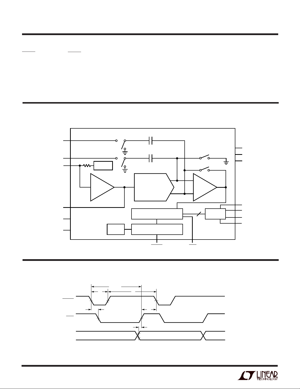
FUNCTIONAL BLOCK DIAGRA
C
+
A
IN
C
–
A
IN
V
REF
2k
2.5V REF
14-BIT CAPACITIVE DAC
AGND (Pin 27): Analog Ground.
AVDD (Pin 28): 5V Positive Supply. Bypass to AGND with
10µ F ceramic or 10µF tantalum in parallel with 0.1µF
ceramic.
SAMPLE
AV
SAMPLE
ZEROING SWITCHES
+
COMPREF AMP
–
DV
V
DD
DD
SS
REFCOMP
(4.06V)
AGND
DGND
UWW
TI I G DIAGRA
CONVST
BUSY
DATA
t
4
t
1
DATA (N – 1)
DB13 TO DB0
INTERNAL
CLOCK
t
CONV
SUCCESSIVE APPROXIMATION
REGISTER
CONTROL LOGIC
CONVST
t
5
t
3
t
2
DB13 TO DB0
DATA N
BUSY
14
OUTPUT
LATCHES
DATA (N + 1)
DB13 TO DB0
1414 BD
1414 TD
OV
DD
D13
•
•
•
D0
OGND
6
 Loading...