

Linear Technology LTC1410 Datasheet
LTC1410
12-Bit, 1.25Msps Sampling
A/D Converter with Shutdown
EATU
F
■
1.25Msps Sample Rate
■
Power Dissipation: 160mW
■
71dB S/(N + D) and 82dB THD at Nyquist
■
No Pipeline Delay
■
Nap (7mW) and Sleep (10µW) Shutdown Modes
■
Operates with Internal 15ppm/°C Reference
RE
S
or External Reference
■
True Differential Inputs Reject Common Mode Noise
■
20MHz Full Power Bandwidth Sampling
■
±2.5V Bipolar Input Range
■
28-Pin SO Wide Package
U
O
PPLICATI
A
■
Telecommunications
■
Digital Signal Processing
■
Multiplexed Data Acquisition Systems
■
High Speed Data Acquisition
■
Spectrum Analysis
■
Imaging Systems
S
DUESCRIPTIO
The LTC®1410 is a 0.65µs, 1.25Msps, 12-bit sampling
A/D converter that draws only 160mW from ±5V supplies.
This easy-to-use device includes a high dynamic range
sample-and-hold, a precision reference and requires no
external components. Two digitally selectable power shutdown modes provide flexibility for low power systems.
The LTC1410’s full-scale input range is ±2.5V. Maximum
DC specifications include ±1LSB INL and ±1LSB DNL over
temperature. Outstanding AC performance includes 71dB
S/(N + D) and 82dB THD at the Nyquist input frequency of
625kHz.
The unique differential input sample-and-hold can acquire
single-ended or differential input signals up to its 20MHz
bandwidth. The 60dB common mode rejection allows
users to eliminate ground loops and common mode noise
by measuring signals differentially from the source.
The ADC has a µ P compatible, 12-bit parallel output port.
There is no pipeline delay in the conversion results. A
separate convert start input and a data ready signal (BUSY)
ease connections to FIFOs, DSPs and microprocessors.
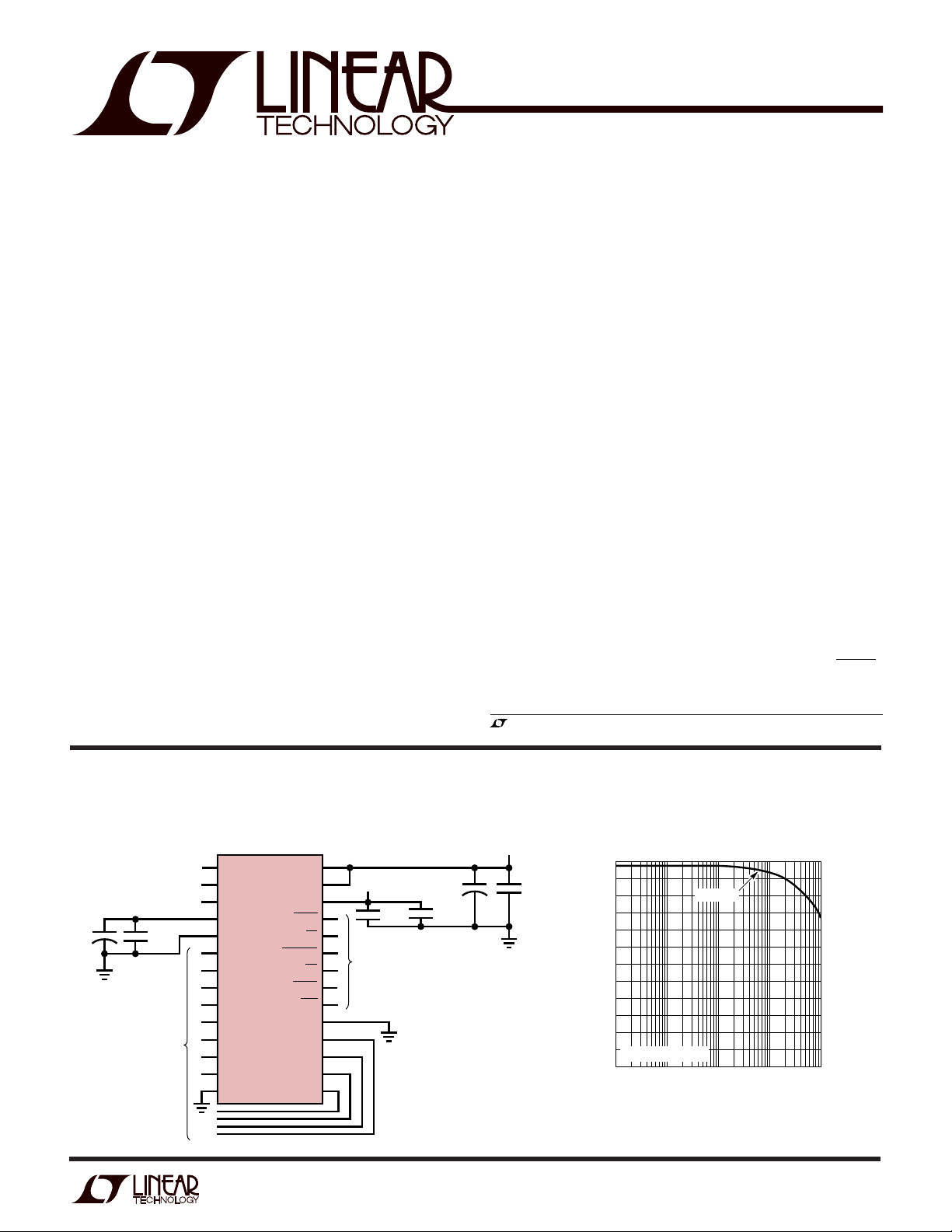
10µF
+
U
O
A
PPLICATITYPICAL
Complete 1.25MHz, 12-Bit Sampling A/D Converter
DIFFERENTIAL
ANALOG INPUT
(–2.5V TO 2.5V)
2.50V
OUTPUT
V
REF
0.1µF
12-BIT
PARALLEL
BUS
10
11
12
13
14
1
+A
2
–A
3
V
4
REFCOMP
5
AGND
6
D11(MSB)
7
D10
8
D9
9
D8
D7
D6
D5
D4
DGND
REF
IN
IN
LTC1410
NAP/SLP
AV
DV
V
BUSY
CONVST
RD
SHDN
OGND
28
DD
27
26
25
24
23
22
21
20
19
18
17
16
15
–5V
10µF
µP CONTROL
LINES
1410 TA01
DD
SS
CS
D0
D1
D2
D3
10µF
0.1µF
, LTC and LT are registered trademarks of Linear Technology Corporation.
Effective Bits and Signal-to-(Noise + Distortion)
vs Input Frequency
5V
+
0.1µF
12 74
10
8
6
EFFECTIVE BITS
4
2
f
SAMPLE
0
1k
NYQUIST
= 1.25MHz
10k 100k 1M 10M
INPUT FREQUENCY (Hz)
LTC1410 • TA02
68
62
56
S/(N + D) (dB)
50
1
LTC1410
W
O
A
AVDD = DVDD = VDD (Notes 1, 2)
LUTEXI T
S
A
WUW
ARB
U
G
I
S
Supply Voltage (VDD)................................................ 6V
Negative Supply Voltage (VSS) ............................... –6V
Total Supply Voltage (VDD to VSS) .......................... 12V
Analog Input Voltage
(Note 3) .................................. VSS – 0.3V to VDD + 0.3V
Digital Input Voltage (Note 4) ............ VSS – 0.3V to 10V
Digital Output Voltage................... – 0.3V to VDD + 0.3V
Power Dissipation............................................. 500mW
Operating Temperature Range
LTC1410C .............................................. 0°C to 70°C
LTC1410I........................................... –40°C to 85°C
Storage Temperature Range................ –65°C to 150°C
Lead Temperature (Soldering, 10 sec)................. 300°C
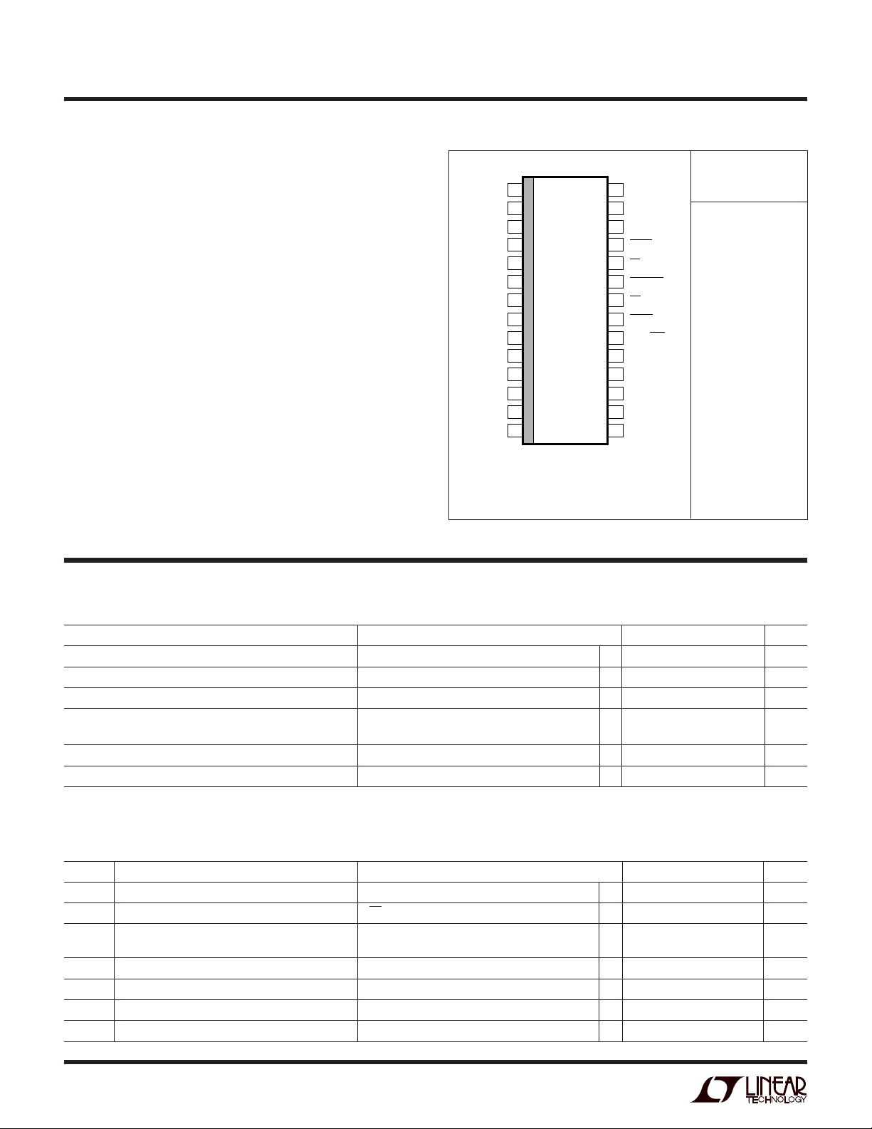
PACKAGE
1
+A
IN
2
–A
IN
3
V
REF
AGND
D10
D9
D8
D7
D6
D5
D4
DGND
G PACKAGE
T
JMAX
T
4
5
6
7
8
9
10
11
12
13
14
= 110°C, θJA = 90°C/W (SW)
= 110°C, θJA = 95°C/W (G)
JMAX
REFCOMP
D11(MSB)
28-LEAD PLASTIC SSOP
/
O
RDER I FOR ATIO
TOP VIEW
28
AV
DD
27
DV
DD
26
V
SS
25
BUSY
24
CS
23
CONVST
22
RD
21
SHDN
20
NAP/SLP
19
OGND
18
D0
17
D1
16
D2
15
D3
SW PACKAGE
28-LEAD PLASTIC SO WIDE
PART NUMBER
LTC1410CG
LTC1410CSW
LTC1410IG
LTC1410ISW
WU
U
ORDER
Consult factory for Military grade parts.
U
U
IN
IN
ACQ
AP
VERTER
CCHARA TERIST
ICS
The ● denotes specifications which apply over the full operating
● ±8 LSB
= 0 ● ±15 ppm/°C
OUT(REF)
U
PUT
LOG
Analog Input Range (Note 9) 4.75V ≤ VDD ≤ 5.25V, –5.25V ≤ VSS ≤ –4.75V ● ±2.5 V
Analog Input Leakage Current CS = High ● ±1 µA
Analog Input Capacitance Between Conversions 17 pF
Sample-and-Hold Acquisition Time ● 50 100 ns
Sample-and-Hold Aperture Delay Time –1.5 ns
Sample-and-Hold Aperture Delay Time Jitter 5 ps
IA
The ● denotes specifications which apply over the full operating temperature range, otherwise
During Conversions 5 pF
RMS
CO
temperature range, otherwise specifications are at TA = 25°C. With Internal Reference (Notes 5, 6)
PARAMETER CONDITIONS MIN TYP MAX UNITS
Resolution (No Missing Codes) ● 12 Bits
Integral Linearity Error (Note 7) ● ±0.3 ±1 LSB
Differential Linearity Error ● ±0.3 ±1 LSB
Offset Error (Note 8) ±2 ±6 LSB
Full-Scale Error ±15 LSB
Full-Scale Tempco I
A
specifications are at TA = 25°C. (Note 5)
SYMBOL PARAMETER CONDITIONS MIN TYP MAX UNITS
V
I
IN
C
t
t
t
jitter
CMRR Analog Input Common Mode Rejection Ratio –2.5V < (–AIN = AIN) < 2.5V 60 dB
2
LTC1410
W
U
DY
A
ACCURAC Y
IC
otherwise specifications are at TA = 25°C. (Note 5)
SYMBOL PARAMETER CONDITIONS MIN TYP MAX UNITS
S/(N + D) Signal-to-(Noise + Distortion) Ratio 100kHz Input Signal (Note 12) ● 70 72.5 dB
THD Total Harmonic Distortion 100kHz Input Signal, First 5 Harmonics –85 dB
Peak Harmonic or Spurious Noise 600kHz Input Signal ● –84 –74 dB
IMD Intermodulation Distortion f
Full Power Bandwidth 20 MHz
Full Linear Bandwidth (S/(N + D) ≥ 68dB) 2.5 MHz
U
UU
I TER AL REFERE CE CHARACTERISTICS
operating temperature range, otherwise specifications are at TA = 25°C. (Note 5)
PARAMETER CONDITIONS MIN TYP MAX UNITS
V
Output Voltage I
REF
V
Output Tempco I
REF
V
Line Regulation 4.75V ≤ VDD ≤ 5.25V 0.01 LSB/V
REF
V
Output Resistance I
REF
COMP Output Voltage I
U
DIGITAL I PUTS A D DIGITAL OUTPUTS
operating temperature range, otherwise specifications are at TA = 25°C. (Note 5)
SYMBOL PARAMETER CONDITIONS MIN TYP MAX UNITS
V
IH
V
IL
I
IN
C
IN
V
OH
V
OL
I
OZ
C
OZ
I
SOURCE
I
SINK
High Level Input Voltage V
Low Level Input Voltage VDD = 4.75V ● 0.8 V
Digital Input Current VIN = 0V to V
Digital Input Capacitance 5pF
High Level Output Voltage VDD = 4.75V
Low Level Output Voltage VDD = 4.75V
High-Z Output Leakage D11 to D0 V
High-Z Output Capacitance D11 to D0 CS High (Note 9 ) ● 15 pF
Output Source Current V
Output Sink Current V
POWER REQUIRE E TS
otherwise specifications are at TA = 25°C. (Note 5)
SYMBOL PARAMETER CONDITIONS MIN TYP MAX UNITS
V
DD
V
SS
I
DD
I
SS
Positive Supply Voltage (Notes 10, 11) 4.75 5.25 V
Negative Supply Voltage (Note 10) –4.75 –5.25 V
Positive Supply Current CS = RD = CONVST = 5V ● 12 16 mA
Nap Mode SHDN = 0V, NAP/SLP = 5V 1.5 2.3 mA
Sleep Mode SHDN = 0V, NAP/SLP = 0V 1 100 µA
Negative Supply Current CS = RD = CONVST = 5V ● 20 30 mA
Nap Mode SHDN = 0V, NAP/SLP = 5V 10 200 µA
Sleep Mode SHDN = 0V, NAP/SLP = 0V 1 100 µA
The ● denotes specifications which apply over the full operating temperature range,
600kHz Input Signal (Note 12)
600kHz Input Signal, First 5 Harmonics
= 29.37kHz, f
IN1
= 32.446kHz –84 dB
IN2
● 68 71.0 dB
● –82 –74 dB
The ● denotes specifications which apply over the full
= 0 2.480 2.500 2.520 V
OUT
= 0 ±15 ppm/°C
OUT
–5.25V ≤ V
OUT
= 0 4.06 V
OUT
≤ –4.75V 0.01 LSB/V
SS
≤ 0.1mA 2 kΩ
U
The ● denotes specifications which apply over the full
= 5.25V ● 2.4 V
DD
● ±10 µA
10 mA
W
U
DD
= –10µA 4.5 V
I
O
IO = –200µA ● 4.0 V
= 160µA 0.05 V
I
O
IO = 1.6mA ● 0.10 0.4 V
= 0V to VDD, CS High ● ±10 µA
OUT
= 0V –10 mA
OUT
= V
OUT
DD
The ● denotes specifications which apply over the full operating temperature range,
3
LTC1410
U
W
POWER REQUIRE E TS
otherwise specifications are at TA = 25°C. (Note 5)
SYMBOL PARAMETER CONDITIONS MIN TYP MAX UNITS
P
D
W
Power Dissipation 160 230 mW
Nap Mode SHDN = 0V, NAP/SLP = 5V 7.5 12 mW
Sleep Mode SHDN = 0V, NAP/SLP = 0V 0.01 1 mW
U
TI I G CHARACTERISTICS
range, otherwise specifications are at TA = 25°C. (Note 5)
SYMBOL PARAMETER CONDITIONS MIN TYP MAX UNITS
f
SAMPLE(MAX)
t
CONV
t
ACQ
t
ACQ+CONV
t
1
t
2
t
3
t
4
t
5
t
6
t
7
t
8
t
9
t
10
t
11
t
12
t
13
t
14
Maximum Sampling Frequency ● 1.25 MHz
Conversion Time ● 650 750 ns
Acquisition Time ● 50 100 ns
Throughput Time ● 800 ns
(Acquisition + Conversion)
CS to RD Setup Time (Notes 9, 10) ● 0ns
CS↓ to CONVST↓ Setup Time (Notes 9, 10) ● 10 ns
NAP/SLP↓ to SHDN ↓ Setup Time (Notes 9, 10) ● 10 ns
SHDN↑ to CONVST↓ Wake-Up Time (Note 10) 200 ns
CONVST Low Time (Notes 10, 11) ● 40 ns
CONVST to BUSY Delay CL = 25pF 10 ns
Data Ready Before BUSY↑ 20 35 ns
Delay Between Conversions (Note 10) ● 40 ns
Wait Time RD↓ After BUSY↑ (Note 10) ● –5 ns
Data Access Time After RD↓ CL = 25pF 15 25 ns
Bus Relinquish Time 820 ns
RD Low Time ● t
CONVST High Time ● 40 ns
Aperture Delay of Sample-and-Hold –1.5 ns
The ● denotes specifications which apply over the full operating temperature range,
The ● denotes specifications which apply over the full operating temperature
● 50 ns
● 15 ns
● 35 ns
C
= 100pF 20 35 ns
L
Commercial ● 25 ns
Industrial
● 50 ns
● 30 ns
10
ns
Note 1: Absolute Maximum Ratings are those values beyond which the life
of a device may be impaired.
Note 2: All voltage values are with respect to ground with DGND, OGND
and AGND wired together unless otherwise noted.
Note 3: When these pin voltages are taken below V
will be clamped by internal diodes. This product can handle input currents
greater than 100mA below V
Note 4: When these pin voltages are taken below VSS, they will be clamped
by internal diodes. This product can handle input currents greater than
100mA below V
Note 5: V
otherwise specified.
Note 6: Linearity, offset and full-scale specifications apply for a singleended +AIN input with –AIN grounded.
without latchup. These pins are not clamped to VDD.
SS
= 5V, VSS = –5V, f
DD
or above VDD without latchup.
SS
= 1.25MHz, tr = tf = 5ns unless
SAMPLE
or above VDD, they
SS
4
Note 7: Integral nonlinearity is defined as the deviation of a code from a
straight line passing through the actual endpoints of the transfer curve.
The deviation is measured from the center of the quantization band.
Note 8: Bipolar offset is the offset voltage measured from –0.5LSB when
the output code flickers between 0000 0000 0000 and 1111 1111 1111.
Note 9: Guaranteed by design, not subject to test.
Note 10: Recommended operating conditions.
Note 11: The falling CONVST edge starts a conversion. If CONVST returns
high at a critical point during the conversion it can create small errors. For
best results ensure that CONVST returns high either within 425ns after the
start of the conversion or after BUSY rises.
Note 12: Signal-to-noise ratio (SNR) is measured at 100kHz and distortion
is measured at 600kHz. These results are used to calculate signal-to-noise
plus distortion (SINAD).
UW
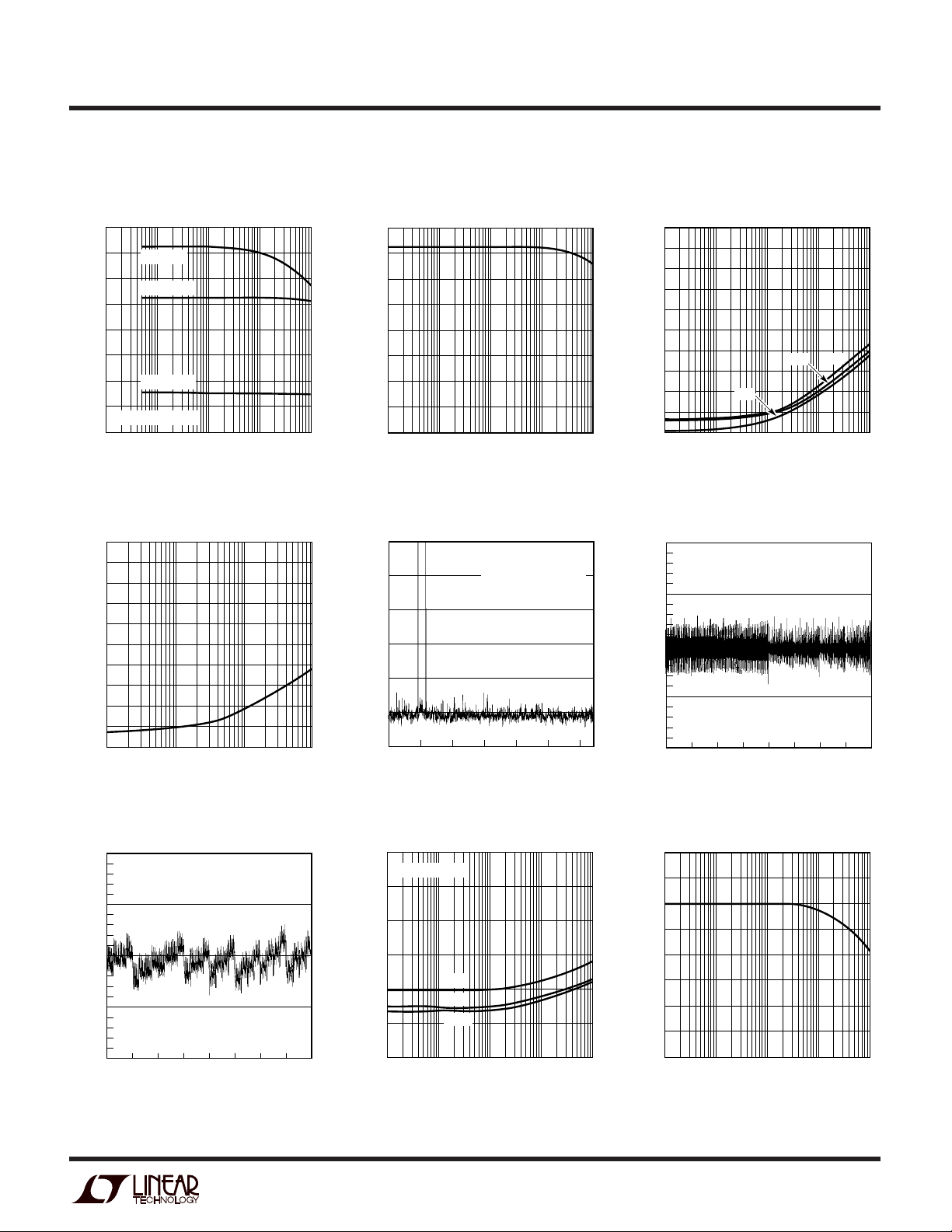
TYPICAL PERFORMAN CE CHAR ACTERISTICS
LTC1410
S/(N + D) vs Input Frequency
and Amplitude
80
70
60
50
40
30
20
10
SIGNAL/(NOISE + DISTORTION) (dB)
VIN = 0dB
VIN = –20dB
VIN = –60dB
f
= 1.25MHz
SAMPLE
0
1k
10k 100k
INPUT FREQUENCY (Hz)
Spurious-Free Dynamic Range vs
Input Frequency
0
–10
–20
–30
–40
–50
–60
–70
–80
–90
SPURIOUS-FREE DYNAMIC RANGE (dB)
–100
10k
100k 1M 10M
INPUT FREQUENCY (Hz)
Integral Nonlinearity vs
Output Code
1.0
0.5
0
INL ERROR (LSB)
–0.5
–1.0
512 1536 2560
0
1024
2048
OUTPUT CODE
1M 10M
1410 G01
1410 G04
3072
3504
4096
1410 G07
Signal-to-Noise Ratio vs
Input Frequency
80
70
60
50
40
30
20
SIGNAL-TO-NOISE RATIO (dB)
10
0
1k
10k 100k
INPUT FREQUENCY (Hz)
1M 10M
1410 G02
Intermodulation Distortion Plot
0
–20
–40
–60
–80
AMPLITUDE (dB)
–100
–120
0
100
f
SAMPLE
= 88.19580078kHz
f
IN1
= 111.9995117kHz
f
IN2
200 300 400
FREQUENCY (kHz)
= 1.25MHz
500 600
1410 G05
Power Supply Feedthrough
vs Ripple Frequency
0
V
= 0.1V
RIPPLE
–20
–40
–60
V
–80
–100
–120
1k 100k 1M 10M
AMPLITUDE OF POWER SUPPLY FEEDTHROUGH (dB)
SS
V
DD
DGND
10k
RIPPLE FREQUENCY (Hz)
1410 G08
Distortion vs Input Frequency
0
–10
–20
–30
–40
–50
–60
–70
–80
–90
AMPLITUDE (dB BELOW THE FUNDAMENTAL)
–100
1k
2ND
10k 100k
INPUT FREQUENCY (Hz)
3RD
1M 10M
Differential Nonlinearity vs
Output Code
1.0
0.5
0
DNL ERROR (LSB)
–0.5
–1.0
512 1536 2560
0
1024
2048
OUTPUT CODE
3072
Input Common Mode Rejection
vs Input Frequency
80
70
60
50
40
30
20
COMMON MODE REJECTION (dB)
10
0
1k
10k 100k
INPUT FREQUENCY (Hz)
1M 10M
THD
3504
1410 G03
4096
1410 G06
1410 G09
5
 Loading...