

FEATURES
■
3Msps Sampling ADC with Two Simultaneous
Differential Inputs
■
1.5Msps Throughput per Channel
■
Low Power Dissipation: 14mW (Typ)
■
3V Single Supply Operation
■
±1.25V Differential Input Range
■
Pin Compatible 0V to 2.5V Input Range Version
(LTC1407/LTC1407A)
■
2.5V Internal Bandgap Reference with External
Overdrive
■
3-Wire Serial Interface
■
Sleep (10µW) Shutdown Mode
■
Nap (3mW) Shutdown Mode
■
80dB Common Mode Rejection at 100kHz
■
Tiny 10-Lead MS Package
U
APPLICATIO S
■
Telecommunications
■
Data Acquisition Systems
■
Uninterrupted Power Supplies
■
Multiphase Motor Control
■
I & Q Demodulation
■
Industrial Radio
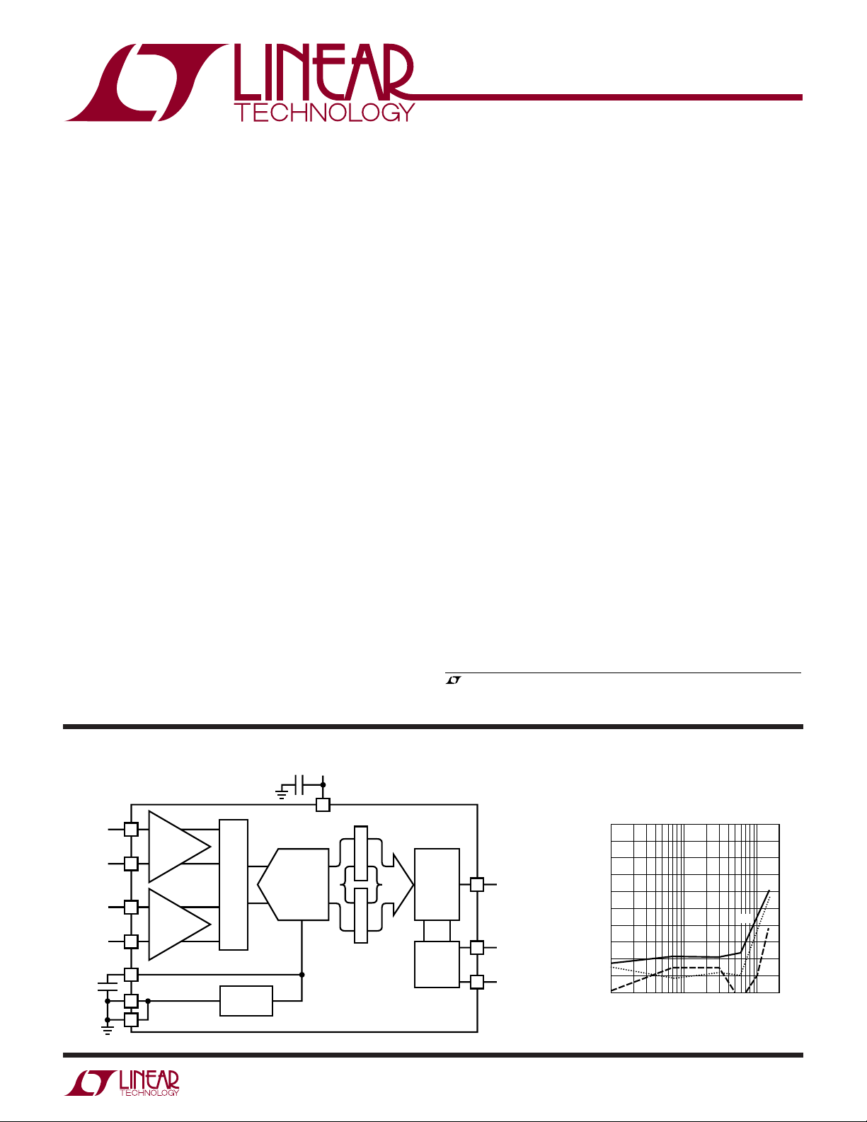
LTC1407-1/LTC1407A-1
Serial 12-Bit/14-Bit, 3Msps
Simultaneous Sampling
ADCs with Shutdown
U
DESCRIPTIO
The LTC®1407-1/LTC1407A-1 are 12-bit/14-bit, 3Msps
ADCs with two 1.5Msps simultaneously sampled differential inputs. The devices draw only 4.7mA from a single 3V
supply and come in a tiny 10-lead MS package. A Sleep
shutdown feature lowers power consumption to 10µW.
The combination of speed, low power and tiny package
makes the LTC1407-1/LTC1407A-1 suitable for high speed,
portable applications.
The LTC1407-1/LTC1407A-1 contain two separate differential inputs that are sampled simultaneously on the rising
edge of the CONV signal. These two sampled inputs are
then converted at a rate of 1.5Msps per channel.
The 80dB common mode rejection allows users to eliminate ground loops and common mode noise by measuring
signals differentially from the source.
The devices convert –1.25V to 1.25V bipolar inputs differentially. The absolute voltage swing for CH0
and CH1– extends from ground to the supply voltage.
The serial interface sends out the two conversion results in
32 clocks for compatibility with standard serial interfaces.
, LT, LTC and LTM are registered trademarks of Linear Technology Corporation.
All other trademarks are the property of their respective owners.
Protected by U.S. Patents, including 6084440, 6522187.
+
, CH0–, CH1
+
BLOCK DIAGRA
+
10µF
CH0
CH0
CH1
CH1
–
+
–
1
2
4
5
3
6
11
+
S & H
–
+
S & H
–
V
REF
GND
EXPOSED PAD
MUX
2.5V
REFERENCE
W
3Msps
14-BIT ADC
3V10µF
THD, 2nd and 3rd vs Input
Frequency for Differential
7
V
DD
14-BIT LATCH14-BIT LATCH
LTC1407A-1
THREE-
STAT E
SERIAL
OUTPUT
PORT
TIMING
LOGIC
8
10
9
1407A1 BD
SDO
CONV
SCK
–44
–50
–56
–62
–68
–74
–80
THD, 2nd, 3rd (dB)
–86
–92
–98
–104
0.1
Input Signals
THD
3rd
2nd
11020
FREQUENCY (MHz)
14071 G22
14071fa
1

LTC1407-1/LTC1407A-1
1
2
3
4
5
CH0
+
CH0
–
V
REF
CH1
+
CH1
–
10
9
8
7
6
CONV
SCK
SDO
V
DD
GND
TOP VIEW
11
MSE PACKAGE
10-LEAD PLASTIC MSOP
CO VERTER CHARACTERISTICS
A ALOG I PUT
WWWU
ABSOLUTE AXI U RATI GS
PACKAGE/ORDER I FOR ATIO
UU
W
(Notes 1, 2)
Supply Voltage (VDD) ................................................. 4V
Analog Input Voltage
(Note 3) ................................... – 0.3V to (V
Digital Input Voltage .................... – 0.3V to (V
Digital Output Voltage .................. – 0.3V to (V
Power Dissipation.............................................. 100mW
Operation Temperature Range
LTC1407C-1/LTC1407AC-1 ..................... 0°C to 70°C
+ 0.3V)
DD
+ 0.3V)
DD
+ 0.3V)
DD
T
= 125°C, θJA = 150°C/ W
EXPOSED PAD IS GND (PIN 11) MUST BE SOLDERED TO PCB
JMAX
ORDER PART NUMBER MSE PART MARKING
LTC1407I-1/LTC1407AI-1 .................. –40°C to 85°C
Storage Temperature Range ................. –65°C to 150°C
Lead Temperature (Soldering, 10 sec).................. 300°C
LTC1407CMSE-1
LTC1407IMSE-1
LTC1407ACMSE-1
LTC1407AIMSE-1
Order Options Tape and Reel: Add #TR
Lead Free: Add #PBF Lead Free Tape and Reel: Add #TRPBF
Lead Free Part Marking: http://www.linear.com/leadfree/
Consult LTC Marketing for parts specified with wider operating temperature ranges.
LTBGT
LTBGV
LTBGW
LTBGX
U
The ● denotes the specifications which apply over the full operating
temperature range, otherwise specifications are at T
PARAMETER CONDITIONS MIN TYP MAX MIN TYP MAX UNITS
Resolution (No Missing Codes)
Integral Linearity Error (Notes 5, 17)
Offset Error (Notes 4, 17)
Offset Match from CH0 to CH1 (Note 17) –5 ±0.5 5 –10 ±110 LSB
Gain Error (Notes 4, 17)
Gain Match from CH0 to CH1 (Note 17) –5 ± 1 5 –10 ±210 LSB
Gain Tempco Internal Reference (Note 4) ± 15 ± 15 ppm/°C
= 25°C. With internal reference, VDD = 3V.
A
LTC1407-1 LTC1407A-1
●
12 14 Bits
●
–2 ±0.25 2 –4 ±0.5 4 LSB
●
–10 ±1 10 –20 ±220 LSB
●
–30 ±5 30 –60 ± 10 60 LSB
External Reference ±1 ±1 ppm/°C
UU
The ● denotes the specifications which apply over the full operating temperature range,
otherwise specifications are at TA = 25°C. With internal reference, VDD = 3V.
SYMBOL PARAMETER CONDITIONS MIN TYP MAX UNITS
V
IN
V
CM
I
IN
C
IN
t
ACQ
t
AP
t
JITTER
t
SK
CMRR Analog Input Common Mode Rejection Ratio fIN = 1MHz, VIN = 0V to 3V –60 dB
2
Analog Differential Input Range (Notes 3, 8, 9) 2.7V ≤ VDD ≤ 3.3V –1.25 to 1.25 V
Analog Common Mode + Differential 0 to V
Input Range (Note 10)
Analog Input Leakage Current
Analog Input Capacitance (Note 18) 13 pF
Sample-and-Hold Acquisition Time (Note 6)
Sample-and-Hold Aperture Delay Time 1 ns
Sample-and-Hold Aperture Delay Time Jitter 0.3 ps
Sample-and-Hold Aperture Skew from CH0 to CH1 200 ps
f
= 100MHz, VIN = 0V to 3V –15 dB
IN
●
●
DD
1 µA
39 ns
14071fa
V

LTC1407-1/LTC1407A-1
U
W
DY A IC ACCURACY
otherwise specifications are at T
–
/CH1– = 1.5V DC. Differential signals drive both inputs of each channel with VCM = 1.5V DC.
CHO
SYMBOL PARAMETER CONDITIONS MIN TYP MAX MIN TYP MAX UNITS
SINAD Signal-to-Noise Plus 100kHz Input Signal (Note 19) 70.5 73.5 dB
Distortion Ratio 750kHz Input Signal (Note 19)
THD Total Harmonic 100kHz First 5 Harmonics (Note 19) –87 –90 dB
Distortion 750kHz First 5 Harmonics (Note 19)
SFDR Spurious Free 100kHz Input Signal (Note 19) 87 90 dB
Dynamic Range 750kHz Input Signal (Note 19) 83 86 dB
IMD Intermodulation 0.625V
Distortion into CH0
Code-to-Code V
Transition Noise
Full Power Bandwidth VIN = 2.5V
Full Linear Bandwidth S/(N + D) ≥ 68dB 5 5 MHz
= 25°C. With internal reference, VDD = 3V. Single ended signal drive CH0+/CH1+ with
A
The ● denotes the specifications which apply over the full operating temperature range,
LTC1407-1 LTC1407A-1
●
68 70.5 70 73.5 dB
100kHz Input Signal, External V
≥ 3.3V (Note 19)
V
DD
750kHz Input Signal, External V
≥ 3.3V (Note 19)
V
DD
1.4MHz Summed with 0.625V
P-P
+
and Inverted into CHO–. Also Applicable
+
and CH1
to CH1
= 2.5V (Note 17) 0.25 1 LSB
REF
–
, SDO = 11585LSB
P-P
= 3.3V, 72.0 76.3 dB
REF
= 3.3V, 72.0 76.3 dB
REF
●
, 1.56MHz –82 –82 dB
P-P
(–3dBFS) (Note 15) 50 50 MHz
P-P
–83 –77 –86 –80 dB
RMS
UU U
I TER AL REFERE CE CHARACTERISTICS
PARAMETER CONDITIONS MIN TYP MAX UNITS
V
Output Voltage I
REF
V
Output Tempco 15 ppm/°C
REF
V
Line Regulation VDD = 2.7V to 3.6V, V
REF
V
Output Resistance Load Current = 0.5mA 0.2 Ω
REF
V
Settling Time 2ms
REF
= 0 2.5 V
OUT
TA = 25°C. VDD = 3V.
= 2.5V 600 µV/V
REF
UU
DIGITAL I PUTS A D DIGITAL OUTPUTS
full operating temperature range, otherwise specifications are at T
SYMBOL PARAMETER CONDITIONS MIN TYP MAX UNITS
V
IH
V
IL
I
IN
C
IN
V
OH
V
OL
I
OZ
C
OZ
I
SOURCE
I
SINK
High Level Input Voltage VDD = 3.3V
Low Level Input Voltage VDD = 2.7V
Digital Input Current VIN = 0V to V
Digital Input Capacitance 5pF
High Level Output Voltage VDD = 3V, I
Low Level Output Voltage VDD = 2.7V, I
= 2.7V, I
V
DD
Hi-Z Output Leakage D
Hi-Z Output Capacitance D
Output Short-Circuit Source Current V
Output Short-Circuit Sink Current V
OUT
OUT
V
OUT
OUT
OUT
= 25°C. VDD = 3V.
A
DD
= –200µA
OUT
OUT
OUT
= 0V to V
= 0V, VDD = 3V 20 mA
= VDD = 3V 15 mA
DD
The ● denotes the specifications which apply over the
●
2.4 V
●
●
●
2.5 2.9 V
= 160µA 0.05 V
= 1.6mA
●
●
0.10 0.4 V
1pF
0.6 V
± 10 µA
± 10 µA
14071fa
3

LTC1407-1/LTC1407A-1
WU
POWER REQUIRE E TS
range, otherwise specifications are at T
SYMBOL PARAMETER CONDITIONS MIN TYP MAX UNITS
V
DD
I
DD
PD Power Dissipation Active Mode with SCK in Fixed State (Hi or Lo) 12 mW
Supply Voltage 2.7 3.6 V
Supply Current Active Mode, f
A
The ● denotes the specifications which apply over the full operating temperature
= 25°C. With internal reference, VDD = 3V.
= 1.5Msps
Nap Mode
Sleep Mode (LTC1407) 2.0 15 µA
Sleep Mode (LTC1407A) 2.0 10 µA
SAMPLE
●
●
4.7 7.0 mA
1.1 1.5 mA
UW
TI I G CHARACTERISTICS
range, otherwise specifications are at T
SYMBOL PARAMETER CONDITIONS MIN TYP MAX UNITS
f
SAMPLE(MAX)
t
THROUGHPUT
t
SCK
t
CONV
t
1
t
2
t
3
t
4
t
5
t
6
t
7
t
8
t
9
t
10
t
12
Note 1: Stresses beyond those listed under Absolute Maximum Ratings
may cause permanent damage to the device. Exposure to any Absolute
Maximum Rating condition for extended periods may affect device
reliability and lifetime.
Note 2: All voltage values are with respect to ground GND.
Note 3: When these pins are taken below GND or above V
clamped by internal diodes. This product can handle input currents greater
than 100mA below GND or greater than V
Note 4: Offset and range specifications apply for a single-ended CH0
+
CH1
input with CH0– or CH1– grounded and using the internal 2.5V
reference.
Note 5: Integral linearity is tested with an external 2.55V reference and is
defined as the deviation of a code from the straight line passing through
the actual endpoints of a transfer curve. The deviation is measured from
the center of quantization band.
Note 6: Guaranteed by design, not subject to test.
Note 7: Recommended operating conditions.
Note 8: The analog input range is defined for the voltage difference
between CH0
–
CHO
= 1.5V DC while driving CHO+ and with CH1– = 1.5V DC while
driving CH1
Note 9: The absolute voltage at CH0
within this range.
Maximum Sampling Frequency per Channel
(Conversion Rate)
Minimum Sampling Period (Conversion + Acquisiton Period)
Clock Period (Note 16)
Conversion Time (Note 6) 32 34 SCLK cycles
Minimum Positive or Negative SCLK Pulse Width (Note 6) 2 ns
CONV to SCK Setup Time (Notes 6, 10) 3 10000 ns
SCK Before CONV (Note 6) 0 ns
Minimum Positive or Negative CONV Pulse Width (Note 6) 4 ns
SCK to Sample Mode (Note 6) 4 ns
CONV to Hold Mode (Notes 6, 11) 1.2 ns
32nd SCK↑ to CONV↑ Interval (Affects Acquisition Period) (Notes 6, 7, 13) 45 ns
Minimum Delay from SCK to Valid Bits 0 Through 11 (Notes 6, 12) 8 ns
SCK to Hi-Z at SDO (Notes 6, 12) 6 ns
Previous SDO Bit Remains Valid After SCK (Notes 6, 12) 2 ns
V
Settling Time After Sleep-to-Wake Transition (Notes 6, 14) 2 ms
REF
+
and CH0– or CH1+ and CH1–. Performance is specified with
+
.
+
, CH0–, CH1+ and CH1– must be
= 25°C. VDD = 3V.
A
without latchup.
DD
The ● denotes the specifications which apply over the full operating temperature
●
1.5 MHz
, they will be
DD
●
●
19.6 10000 ns
Note 10: If less than 3ns is allowed, the output data will appear one clock
cycle later. It is best for CONV to rise half a clock before SCK, when
running the clock at rated speed.
Note 11: Not the same as aperture delay. Aperture delay (1ns) is the
difference between the 2.2ns delay through the sample-and-hold and the
1.2ns CONV to Hold mode delay.
Note 12: The rising edge of SCK is guaranteed to catch the data coming
out into a storage latch.
+
or
Note 13: The time period for acquiring the input signal is started by the
32nd rising clock and it is ended by the rising edge of CONV.
Note 14: The internal reference settles in 2ms after it wakes up from Sleep
mode with one or more cycles at SCK and a 10µF capacitive load.
Note 15: The full power bandwidth is the frequency where the output code
swing drops by 3dB with a 2.5V
Note 16: Maximum clock period guarantees analog performance during
conversion. Output data can be read with an arbitrarily long clock period.
Note 17: The LTC1407A-1 is measured and specified with 14-bit
Resolution (1LSB = 152µV) and the LTC1407-1 is measured and specified
with 12-bit Resolution (1LSB = 610µV).
Note 18: The sampling capacitor at each input accounts for 4.1pF of the
input capacitance.
Note 19: Full-scale sinewaves are fed into the noninverting inputs while
the inverting inputs are kept at 1.5V DC.
input sine wave.
P-P
667 ns
14071fa
4

UW
FREQUENCY (MHz)
0.1
68
SFDR (dB)
56
44
1 10 100
14071 G03
80
74
62
50
86
92
98
104
FREQUENCY (kHz)
0
MAGNITUDE (dB)
–60
–30
–20
14071 G06
–70
–80
–120
200 400100 300 600500 700
–100
0
–10
–40
–50
–90
–110
TYPICAL PERFOR A CE CHARACTERISTICS
+CH0/+CH1 with –CH0/–CH1 = 1.5V DC, differential signals drive both inputs with V
V
DD
CM
LTC1407-1/LTC1407A-1
= 3V, TA = 25°C. Single ended signals drive
= 1.5V DC (LTC1407A-1)
ENOBs and SINAD
vs Input Sinewave Frequency
12.0
11.5
11.0
10.5
10.0
9.5
ENOBs (BITS)
9.0
8.5
8.0
0.1
1 10 100
FREQUENCY (MHz)
SNR vs Input Frequency
74
71
68
65
62
SNR (dB)
59
56
53
50
0.1
1 10 100
FREQUENCY (MHz)
14071 G01
14071 G04
74
71
68
SINAD (dB)
65
62
59
56
53
50
12.0
11.5
11.0
10.5
10.0
9.5
ENOBs (BITS)
9.0
8.5
8.0
THD, 2nd and 3rd
vs Input Frequency
–44
–50
–56
–62
–68
–74
–80
THD, 2nd, 3rd (dB)
–86
–92
–98
–104
0.1
THD
2nd
1 10 100
FREQUENCY (MHz)
ENOBs and SINAD vs Input
Sinewave Frequency for
Differential Input Signals
0.1
1 10 100
FREQUENCY (MHz)
3rd
14071 G21
14071 G02
74
71
68
65
62
59
56
53
50
SINAD (dB)
THD, 2nd, 3rd (dB)
–104
SFDR vs Input Frequency
THD, 2nd and 3rd vs Input
Frequency for Differential Input
Signals
–44
–50
–56
–62
–68
–74
–80
–86
–92
–98
0.1
11020
FREQUENCY (MHz)
THD
3rd
2nd
14071 G22
SFDR vs Input Frequency for
Differential Input Signals
104
98
92
86
80
74
SFDR (dB)
68
62
56
50
44
0.1
1 10 100
FREQUENCY (MHz)
14071 G23
98kHz Sine Wave 4096 Point
FFT Plot
0
–10
–20
–30
–40
–50
–60
–70
MAGNITUDE (dB)
–80
–90
–100
–110
–120
0
200 400100 300 600500 700
FREQUENCY (kHz)
748kHz Sine Wave 4096 Point
FFT Plot
14071 G05
14071fa
5
LTC1407-1/LTC1407A-1
FREQUENCY (Hz)
MAGNITUDE (dB)
–60
–30
–20
14071 G25
–70
–80
–120
–100
0
–10
–40
–50
–90
–110
0
371k185k 556k 741k
UW
TYPICAL PERFOR A CE CHARACTERISTICS
+CH0/+CH1 with –CH0/–CH1 = 1.5V DC, differential signals drive both inputs with V
VDD = 3V, TA = 25°C. Single ended signals drive
CM
= 1.5V DC (LTC1407A-1)
MAGNITUDE (dB)
–100
–110
–120
–0.2
–0.4
–0.6
DIFFERENTIAL LINEARITY (LSB)
–0.8
–1.0
–0.2
–0.4
–0.6
DIFFERENTIAL LINEARITY (LSB)
–0.8
–1.0
6
1403kHz Input Summed with
1563kHz Input IMD 4096 Point FFT
Plot for Differential Input Signals
0
–10
–20
–30
–40
–50
–60
–70
–80
–90
0
200 400100 300 600500 700
FREQUENCY (kHz)
Differential Linearity for CH0 with
Internal 2.5V Reference
1.0
0.8
0.6
0.4
0.2
0
0
4096
8192
OUTPUT CODE
12288
Differential Linearity for CH1 with
Internal 2.5V Reference
1.0
0.8
0.6
0.4
0.2
0
0
4096
OUTPUT CODE
8192
12288
14071 G07
16384
14071 G08
16384
14071 G10
748kHz Sine Wave 4096 Point FFT
Plot for Differential Input Signals
0
–10
–20
–30
–40
–50
–60
–70
MAGNITUDE (dB)
–80
–90
–100
–110
–120
0
371k185k 556k 741k
FREQUENCY (Hz)
Integral Linearity End Point Fit for
CH0 with Internal 2.5V Reference
4.0
3.2
2.4
1.6
0.8
0
–0.8
–1.6
INTEGRAL LINEARITY (LSB)
–2.4
–3.2
–4.0
0
4096
8192
OUTPUT CODE
12288
Integral Linearity End Point Fit for
CH1 with Internal 2.5V Reference
4.0
3.2
2.4
1.6
0.8
0
–0.8
–1.6
INTEGRAL LINEARITY (LSB)
–2.4
–3.2
–4.0
0
4096
8192
OUTPUT CODE
12288
14071 G24
16384
14071 G09
16384
14071 G11
10.7MHz Sine Wave 4096 Point
FFT Plot for Differential Input
Signals
Integral Linearity End Point Fit for
CH0 with Internal 2.5V Reference
for Differential Input Signals
4.0
3.2
2.4
1.6
0.8
0
–0.8
–1.6
INTEGRAL LINEARITY (LSB)
–2.4
–3.2
–4.0
0
4096
8192
OUTPUT CODE
12288
Integral Linearity End Point Fit for
CH1 with Internal 2.5V Reference
for Differential Input Signals
4.0
3.2
2.4
1.6
0.8
0
–0.8
–1.6
INTEGRAL LINEARITY (LSB)
–2.4
–3.2
–4.0
0
4096
8192
OUTPUT CODE
12288
16384
14071 G26
16384
14071 G27
14071fa
UW
TYPICAL PERFOR A CE CHARACTERISTICS
+CH0/+CH1 with –CH0/–CH1 = 1.5V DC, differential signals drive both inputs with V
Differential and Integral Linearity
vs Conversion Rate
8
7
6
5
3 3.25
14071 G14
10
TIME (ns)
MAX INL
MAX DNL
3.5 3.75
CMRR (dB)
–100
–120
CH0 AND CH1
RISING
CH0 AND CH1
FALLING
4
14071 G12
CMRR vs Frequency Crosstalk vs Frequency
0
–20
–40
–60
–80
100 1k
CH0
CH1
20
14071 G17
25
CH0 CH1
10k 100k 1M 10M 100M
FREQUENCY (Hz)
4
3
2
1
LINEARITY (LSB)
0
–1
–2
–3
–4
= 3V, TA = 25°C (LTC1407-1/LTC1407A-1)
V
DD
MIN DNL
MIN INL
2
2.5 2.752.25
CONVERSION RATE (MSPS)
Full-Scale Signal Frequency
Response
12
6
0
–6
–12
–18
AMPLITUDE (dB)
–24
–30
–36
1M 10M 100M 1G
FREQUENCY (Hz)
Output Match with Simultaneous
Input Steps at CH0 and CH1 from
25Ω
16384
14336
12288
10240
8192
6144
OUTPUT CODE
4096
2048
0
05 15
–5
VDD = 3V, TA = 25°C. Single ended signals drive
CM
SINAD vs Conversion Rate
78
77
76
75
74
73
72
S/(N+D) (dB)
71
70
69
68
2 2.5 3 3.5 4
14071 G15
PSSR vs Frequency
–25
–30
–35
–40
–45
–50
PSRR (dB)
–55
–60
–65
–70
110
LTC1407-1/LTC1407A-1
= 1.5V DC (LTC1407A-1)
EXTERNAL V
EXTERNAL V
INTERNAL V
INTERNAL V
CONVERSION RATE (Msps)
= 3.3V, fIN ~ fS/3
REF
= 3.3V, fIN ~ fS/40
REF
= 2.5V, fIN ~ fS/3
REF
= 2.5V, fIN ~ fS/40
REF
14071 G13
–20
–30
–40
–50
–60
CROSSTALK (dB)
–70
CH0 TO CH1
–80
–90
100 1k 10k 100k 1M 10M
100 1k 10k 100k 1M
FREQUENCY (Hz)
CH1 TO CH0
FREQUENCY (Hz)
14071 G18
14071 G16
14071fa
7

LTC1407-1/LTC1407A-1
UW
TYPICAL PERFOR A CE CHARACTERISTICS
Reference Voltage vs V
2.4902
DD
2.4902
VDD = 3V, TA = 25°C (LTC1407-1/LTC1407A-1)
Reference Voltage
vs Load Current
2.4900
2.4898
(V)
2.4896
REF
V
2.4894
2.4892
2.4890
2.6 3.6
U
2.8 3.0 3.2 3.4
UU
VDD (V)
14071 G19
PI FU CTIO S
CH0+ (Pin 1): Noninverting Channel 0. CH0+ operates fully
differentially with respect to CH0
differential swing with respect to CH0
absolute input range.
–
(Pin 2): Inverting Channel 0. CH0– operates fully
CH0
differentially with respect to CH0
differential swing with respect to CH0+ and a 0 to V
absolute input range.
V
(Pin 3): 2.5V Internal Reference. Bypass to GND and
REF
a solid analog ground plane with a 10µF ceramic capacitor
(or 10µF tantalum in parallel with 0.1µF ceramic). Can be
overdriven by an external reference voltage ≥2.55V and
≤VDD.
CH1+ (Pin 4): Noninverting Channel 1. CH1+ operates fully
differentially with respect to CH1
differential swing with respect to CH1
absolute input range.
CH1– (Pin 5): Inverting Channel 1. CH1– operates fully
differentially with respect to CH1+, with a 1.25V to –1.25V
differential swing with respect to CH1
absolute input range.
GND (Pins 6, 11): Ground and Exposed Pad. This single
ground pin and the Exposed Pad must be tied directly to
–
, with a –1.25V to 1.25V
–
and a 0 to V
+
, with a 1.25V to –1.25V
–
, with a –1.25V to 1.25V
–
and a 0 to V
+
and a 0 to V
DD
DD
DD
DD
2.4900
2.4898
(V)
2.4896
REF
V
2.4894
2.4892
2.4890
0.4 0.8 1.2 1.6
LOAD CURRENT (mA)
2.00.20 0.6 1.0 1.4 1.8
14071 G20
the solid ground plane under the part. Keep in mind that
analog signal currents and digital output signal currents
flow through these connections.
(Pin 7): 3V Positive Supply. This single power pin
V
DD
supplies 3V to the entire chip. Bypass to GND pin and solid
analog ground plane with a 10µF ceramic capacitor (or
10µF tantalum) in parallel with 0.1µF ceramic. Keep in
mind that internal analog currents and digital output signal
currents flow through this pin. Care should be taken to
place the 0.1µF bypass capacitor as close to Pins 6 and 7
as possible.
SDO (Pin 8): Three-state Serial Data Output. Each pair of
output data words represent the two analog input channels at the start of the previous conversion. The output
format is 2’s complement.
SCK (Pin 9): External Clock Input. Advances the conversion process and sequences the output data on the rising
edge. One or more pulses wake from sleep.
CONV (Pin 10): Convert Start. Holds the two analog input
signals and starts the conversion on the rising edge. Two
pulses with SCK in fixed high or fixed low state starts Nap
mode. Four or more pulses with SCK in fixed high or fixed
low state starts Sleep mode.
14071fa
8
 Loading...