

Linear Technology LTC1402 Datasheet
FEATURES
Final Electrical Specifications
■
Sample Rate: 2.2Msps
■
72dB S/(N + D) and –89dB THD at Nyquist
■
No Missing Codes over Temperature
■
Available in 16-Pin Narrow SSOP Package
■
Single Supply 5V or ±5V Operation
■
Power Dissipation: 90mW (Typ)
■
Nap Mode with Instant Wake-Up: 15mW
■
Sleep Mode: 10µW
■
True Differential Inputs Reject Common Mode Noise
■
80MHz Full Power Bandwidth Sampling
■
Input Range (1mV/LSB): 0V to 4.096V or ±2.048V
■
Internal Reference Can Be Overdriven Externally
■
3-Wire Interface to DSPs and Processors (SPI and
MICROWIRETM Compatible)
U
APPLICATIONS
■
Telecommunications
■
High Speed Data and Signal Acquisition
■
Digitally Multiplexed Data Acquisition Systems
■
Digital Radio Receivers
■
Spectrum Analysis
■
Low Power and Battery-Operated Systems
■
Handheld or Portable Instruments
■
Imaging Systems
, LTC and LT are registered trademarks of Linear Technology Corporation.
MICROWIRE is a trademark of National Semiconductor Corp.
LTC1402
Serial 12-Bit, 2.2Msps
Sampling ADC with Shutdown
U
DESCRIPTION
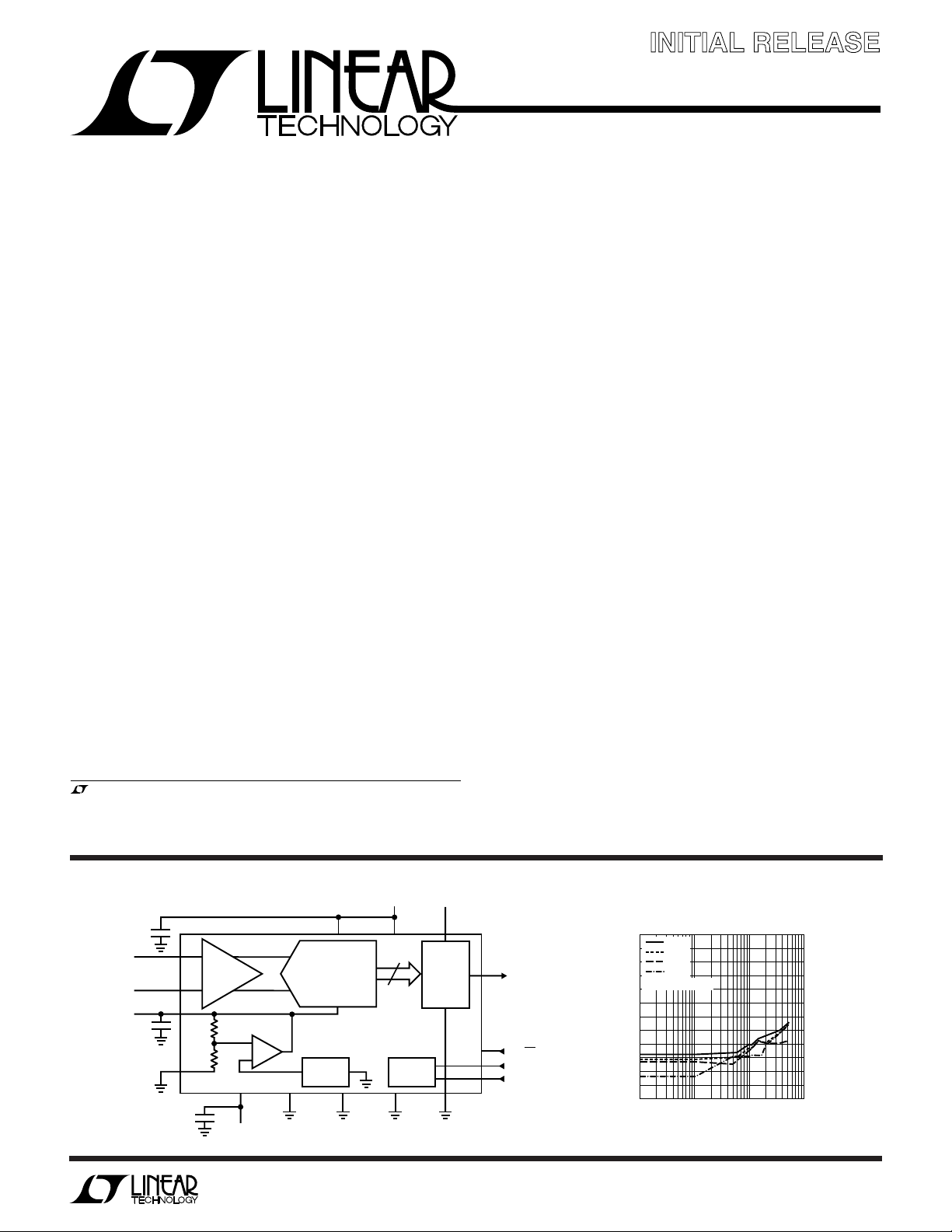
The LTC®1402 is a 12-bit, 2.2Msps sampling A/D converter. This high performance device includes a high dynamic range sample-and-hold and a precision reference.
It operates from a single 5V supply or dual ±5V supplies
and draws only 90mW from 5V.
The versatile differential input offers a unipolar range of
4.096V and a bipolar range of ±2.048V for dual supply
systems where high performance op amps perform best,
eliminating the need for special translation circuitry.
The high common mode rejection allows users to eliminate ground loops and common mode noise by measuring
signals differentially from the source.
Outstanding AC performance includes 72dB S/(N + D) and
–93dB SFDR at the Nyquist input frequency of 1.1MHz
with dual ±5V supplies and –84dB SFDR with a single 5V
supply.
The LTC1402 has two power saving modes: Nap and
Sleep. Nap mode consumes only 15mW of power and
Sleep can wake up and convert immediately. In Sleep
mode, it typically consumes 10µW of power. Upon power-
up from Sleep mode, a reference ready (REFRDY) signal
is available in the serial data word to indicate that the
reference has settled and the chip is ready to convert.
The 3-wire serial port allows compact and efficient data
transfer to a wide range of microprocessors, microcontrollers and DSPs. A digital output driver power supply pin
allows direct connection to 3V or lower logic.
October 1999
BLOCK DIAGRA
10µF
10µF
GAIN
3
SAMPLE-
AND-HOLD
4
5
7
LTC1402
10µF
+A
IN
–A
IN
V
REF
4.096V
64k
64k
–5V OR 0V
W
5V 3V OR 5V
AVDD11211
12-BIT ADC
–
+
2.048
REFERENCE
AGND1VSS14 13AGND2
Information furnished by Linear Technology Corporation is believed to be accurate and reliable.
However, no responsibility is assumed for its use. Linear Technology Corporation makes no representation that the interconnection of its circuits as described herein will not infringe on existing patent rights.
DV
TIMING
LOGIC
OV
OUTPUT
BUFFER
DD
10
D
OUT
8
BIP/UNI
16
CONV
15
SCK
1402 TA01
OGND962 DGND
DD
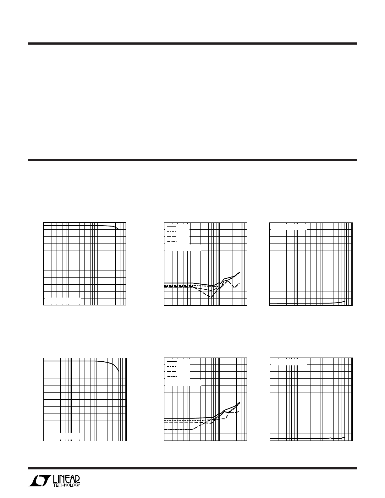
5 Harmonic THD, 2nd, 3rd and SFDR
vs Input Frequency (Unipolar)
0
–10
–20
–30
f
SAMPLE
–40
–50
–60
–70
–80
–90
THD, SFDR, 2ND 3RD (dB)
–100
–110
–120
4
10
THD
SFDR
2ND
3RD
= 2.22MHz
5
10
INPUT FREQUENCY (Hz)
6
10
1401 G05
7
10
1
LTC1402
T
WW
W
U
ABSOLUTE MAXIMUM RATINGS
AVDD = DVDD = OVDD = V
Supply Voltage (VDD)................................................. 6V
Negative Supply Voltage (VSS) ............................... – 6V
Total Supply Voltage (VDD to VSS) .......................... 12V
Analog Input Voltage
(Note 3) ..........................(VSS – 0.3V) to (VDD + 0.3V)
Digital Input Voltage
(Note 4) ..........................(VSS – 0.3V) to (VDD + 0.3V)
Digital Output Voltage......... (VSS – 0.3V) to (VDD + 0.3V)
Power Dissipation.............................................. 250mW
Operation Temperature Range
LTC1402C ............................................... 0°C to 70°C
LTC1402I............................................ –40°C to 85°C
Storage Temperature Range ................. –65°C to 150°C
(Notes 1, 2)
DD
U
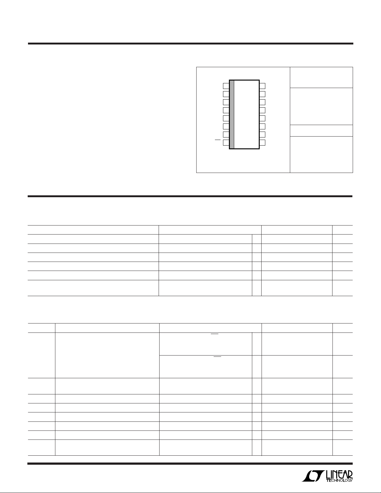
PACKAGE/ORDER INFORMATION
TOP VIEW
AV
1
DD
2
AGND1
+
3
A
IN
–
4
A
IN
5
V
REF
6
AGND2
7
GAIN
8
BIP/UNI
16-LEAD NARROW PLASTIC SSOP
Consult factory for Military grade parts.
GN PACKAGE
T
= 125°C, θJA = 150°C/W
JMAX
CONV
16
15
SCK
14
V
SS
13
DGND
12
DV
DD
11
0V
DD
10
D
OUT
9
OGND
GN PART MARKING
W
ORDER PART
NUMBER
LTC1402CGN
LTC1402IGN
1402
1402I
U
Lead Temperature (Soldering, 10 sec).................. 300°C
U
CONVERTER CHARACTERISTICS
temperature range, otherwise specifications are at TA = 25°C. With internal reference (Note 5).
PARAMETER CONDITIONS MIN TYP MAX UNITS
Resolution (No Missing Codes) ● 12 Bits
Integral Linearity Error (Note 6) ● ±0.35 ±1LSB
Differential Linearity (Note 6) ● ±0.25 ±1LSB
Offset Error (Note 6) ● ±2 ±10 LSB
Full-Scale Error (Note 6) ● ±10 ±15 LSB
Full-Scale Tempco Internal Reference (Note 6) ±15 ppm/°C
The ● denotes the specifications which apply over the full operating
External Reference ±1 ppm/°C
UU
A ALOG I PU
otherwise specifications are at TA = 25°C. (Note 5)
The ● denotes the specifications which apply over the full operating temperature range,
SYMBOL PARAMETER CONDITIONS MIN TYP MAX UNITS
V
IN
V
CM
I
IN
C
IN
t
ACQ
t
AP
t
JITTER
CMRR Analog Input Common Mode Rejection Ratio fIN = 1MHz, VIN = 2V to –2V –62 dB
Analog Differential Input Range (Notes 3, 11) Bipolar Mode with BIP/UNI High ● ±2.048 V
4.75V ≤ V
–5.25V ≤ V
Unipolar Mode with BIP/UNI Low ● 0 to 4.096 V
4.75V ≤ V
–5.25V ≤ V
Analog Common Mode + Differential Dual ±5V Supply –2.5 to 5 V
Input Range (Note 12) Single 5V Supply 0 to 5 V
Analog Input Leakage Current ● 1 µA
Analog Input Capacitance 10 pF
Sample-and-Hold Acquisition Time ● 60 ns
Sample-and-Hold Aperture Delay Time 2.6 ns
Sample-and-Hold Aperture Delay Time Jitter 1 ps
f
= 100MHz, VIN = 2V to –2V –24 dB
IN
≤ 5.25V V
DD
≤ –4.75V V
SS
≤ 5.25V V
DD
≤ 0V V
SS
2
LTC1402
UW
DYNAMIC ACCURACY
otherwise specifications are at TA = 25°C. Bipolar mode with ± 5V supplies and unipolar mode with 5V supply. (Note 5)
SYMBOL PARAMETER CONDITIONS MIN TYP MAX UNITS
S/(N + D) Signal-to-Noise Plus 100kHz Input Signal 72.5 dB
Distortion Ratio 1.1MHz Input Signal
THD Total Harmonic 100kHz First 5 Harmonics, Bipolar Mode –89 dB
Distortion 1.1MHz First 5 Harmonics, Bipolar Mode
100kHz First 5 Harmonics, Unipolar Mode –87 dB
1.1MHz First 5 Harmonics, Unipolar Mode –82 dB
SFDR Spurious Free 1.1MHz Input Signal in Bipolar Mode –93 dB
Dynamic Range 1.1MHz Input Signal in Unipolar Mode –84 dB
IMD Intermodulation ±1V 1.25MHz into A
Distortion 1.5V to 3.5V 1.25MHz into A
Code-to-Code V
Transition Noise
Full Power Bandwidth VIN = 4V
Full Linear Bandwidth S/(N + D) ≥ 68dB Bipolar Mode 5.0 MHz
Unipolar Mode 3.5 MHz
The ● denotes the specifications which apply over the full operating temperature range,
● 69 72.0 dB
● –89 –74.5 dB
+
, 1.2MHz into A
IN
= 4.096V, 1LSB = 1mV 0.18 LSB
REF
, D
OUT
= 2828
P-P
+
IN
(Note 18) 82 MHz
P-P
–
Bipolar Mode –84 dB
IN
, 1.2MHz into A
–
Unipolar Mode –84 dB
IN
RMS
UU U
INTERNAL REFERENCE CHARACTERISTICS
full operating temperature range, otherwise specifications are at TA = 25°C. (Note 5)
The ● denotes the specifications which apply over the
PARAMETER CONDITIONS MIN TYP MAX UNITS
V
Output Voltage I
REF
V
Output Tempco 15 ppm/°C
REF
V
Line Regulation AVDD = 4.75V to 5.25V, V
REF
V
Output Resistance Load Current = 0.5mA 2 Ω
REF
V
Settling Time 2ms
REF
= 0 4.096 V
OUT
= 4.096V 1 LSB/V
REF
UU
DIGITAL I PUTS A D DIGITAL OUTPUTS
full operating temperature range, otherwise specifications are at TA = 25°C. (Note 5)
SYMBOL PARAMETER CONDITIONS MIN TYP MAX UNITS
V
IH
V
IL
I
IN
C
IN
V
OH
V
OL
I
OZ
C
OZ
I
SOURCE
I
SINK
High Level Input Voltage VDD = 5.25V ● 2.4 V
Low Level Input Voltage VDD = 4.75V ● 0.8 V
Digital Input Current VIN = 0V to V
Digital Input Capacitance 5pF
High Level Output Voltage OVDD = 4.75V, I
OV
DD
OV
DD
Low Level Output Voltage VDD = 4.75V, I
V
= 4.75V, I
DD
Hi-Z Output Leakage D
Hi-Z Output Capacitance D
Output Short-Circuit Source Current V
Output Short-Circuit Sink Current V
OUT
OUT
V
OUT
OUT
V
OUT
OUT
DD
= 4.75V, I
= 3V, I
= 0V to V
= 0V, OVDD = 5V –40 mA
= 0V, OVDD = 3V –15 mA
= OVDD = 5V 40 mA
OUT
OUT
OUT
OUT
OUT
DD
The ● denotes the specifications which apply over the
● ±10 µA
= –10µA 4.7 V
= –200µA ● 4V
= –200µA ● 2.5 2.9 V
= 160µA 0.05 V
= 1.6mA ● 0.10 0.4 V
● ±10 µA
15 pF
3
LTC1402
WU
POWER REQUIRE E TS
range, otherwise specifications are at TA = 25°C. (Note 5)
SYMBOL PARAMETER CONDITIONS MIN TYP MAX UNITS
V
DD
V
SS
I
DD
I
SS
PD Power Dissipation Active Mode with SCK in Fixed State (Hi or Lo) 90 150 mW
Positive Supply Voltage 4.75 5.00 5.25 V
Negative Supply Voltage –5.25 –5.00 0 V
Positive Supply Current Active Mode ● 18 30 mA
Negative Supply Current Active, Sleep or Nap Modes with SCK Off ● 2 µA
The ● denotes the specifications which apply over the full operating temperature
Nap Mode
Sleep Mode 2 10 µA
● 35 mA
UW
TI I G CHARACTERISTICS
range, otherwise specifications are at TA = 25°C. (Note 5)
SYMBOL PARAMETER CONDITIONS MIN TYP MAX UNITS
f
SAMPLE(MAX)
t
THROUGHPUT
t
SCK
t
CONV
t
ACQ
t
1
t
2
t
3
t
4
t
5
t
6
t
7
t
8
t
8a
t
9
t
10
t
11
t
12
Maximum Sampling Frequency (Conversion Rate) ● 2.2 MHz
Minimum Sampling Period (Conversion + Acquisiton Period) ● 455 ns
Minimum Clock Period ● 28 10000 ns
Conversion Time Greater Than 13 Clocks + 6ns (Note 9) ● 375 ns
Acquisition Time Greater Than 2 Clocks – 6ns (Notes 9, 16) ● 51 ns
Minimum Positive or Negative SCK Pulse Width (Note 9) ● 3.8 6 ns
CONV to SCK Setup Time (Notes 9, 13) ● 7.3 12 ns
SCK After CONV (Note 9) ● 0ns
Minimum Positive or Negative CONV Pulse Width (Note 9) ● 3.5 5 ns
SCK to Sample Mode (Notes 9, 14) ● 914 ns
CONV to Hold Mode (Note 9) ● 3.4 5 ns
Minimum Delay Between Conversions (Note 9) ● 48 ns
Minimum Delay from SCK to Valid Bits 0 Through 11 (Notes 9, 15) ● 912 ns
Minimum Delay from SCK to Valid REFREADY (Notes 9, 15) ● 15 20 ns
SCK to Hi-Z at D
Previous D
REFREADY Bit Delay After Sleep-to-Wake Transition (Notes 9, 17) ● 10 ms
V
Settling Time After Sleep-to-Wake Transition (Notes 9, 17) ● 2ms
REF
OUT
Bit Remains Valid After SCK (Notes 9, 15) ● 47 ns
OUT
The ● denotes the specifications which apply over the full operating temperature
(Notes 9, 15) ● 11.4 16 ns
Note 1: Absolute Maximum Ratings are those values beyond which the life
of a device may be impaired.
Note 2: All voltage values are with respect to ground with DGND, AGND1
and AGND2 wired together.
Note 3: When these pins are taken below V
clamped by internal diodes. This product can handle input currents greater
than 100mA below V
Note 4: When these pins are taken below VSS, they will be clamped by
internal diodes. This product can handle input currents greater than
100mA below VSS or greater than VDD. These pins are not clamped to VDD.
Note 5: V
specifications and V
= 5V, f
DD
or greater than VDD without latchup.
SS
= 2.2MHz, VSS = 0V for unipolar mode
SAMPLE
= –5V for bipolar specifications.
SS
or above VDD, they will be
SS
4
Note 6: Linearity, offset and full-scale specifications apply for a singleended A
bipolar mode with ±5V supplies.
Note 7: Integral linearity is defined as the deviation of a code from the
straight line passing through the actual endpoints of a transfer curve. The
deviation is measured from the center of quantization band.
Note 8: Bipolar offset is the offset measured from –0.5LSB when the input
flickers between 1000 0000 0000 and 0111 1111 1111.
Note 9: Guaranteed by design, not subject to test.
Note 10: Recommended operating conditions.
Note 11: The analog input range is defined as the voltage difference
between A
with a single 5V supply if the absolute voltages of the inputs remain within
the single 5V supply voltage.
+
input with A
IN
+
and A
IN
–
grounded and using the internal reference in
IN
–
. The bipolar ±2.048V input range could be used
IN
LTC1402
ELECTRICAL CHARACTERISTICS
Note 12: The absolute voltage at A
+
IN
Note 13: If less than 7.3ns is allowed, the output data will appear one
clock cycle later. It is best for CONV to rise half a clock before SCK, when
running the clock at rated speed.
Note 14: Not the same as aperture delay. Aperture delay is smaller (2.6ns)
because the 0.8ns delay through the sample-and-hold is subtracted from
the CONV to Hold mode delay.
Note 15: The rising edge of SCK is guaranteed to catch the data coming
out into a storage latch.
Note 16: The Sample mode is started by the 14th rising clock and it is
ended by the rising edge of convert. Because the start of Sample mode is
and A
–
must be within this range.
IN
slower than the end of Sample mode, the sample time is 6ns less than the
delay between the 14th SCK and CONV.
Note 17: The internal reference settles in 2ms after it wakes up from Sleep
mode with one or more cycles at SCK and a 10µF capacitive load. The
Sleep mode resets the REFREADY bit in the D
REFREADY bit goes high again 10ms after the V
sequence. The
OUT
has stopped slewing in
REF
wake up. This ensures valid REFREADY bit operation even with higher load
capacitances at V
REF
.
Note 18: The full power bandwidth is the frequency where the output code
swing drops to 2828LSBs with a 4V
input sine wave.
P-P
UW
TYPICAL PERFOR A CE CHARACTERISTICS
Unipolar Mode Plots Run with a Single 5V Supply. VDD = 5V, VSS = –5V for Bipolar, VDD = 5V, VSS = 0V for Unipolar), TA = 25°C.
5 Harmonic THD, 2nd, 3rd and
ENOBs and SINAD
vs Input Frequency (Bipolar)
12
11
10
9
8
7
6
5
4
3
EFFECTIVE NUMBER OF BITS
2
1
f
= 2.22MHz
SAMPLE
0
4
10
5
10
INPUT FREQUENCY (Hz)
74
SIGNAL-TO-NOISE + DISTORTION (dB)
68
62
56
50
44
38
32
26
20
14
8
1401 G01
2
7
10
6
10
SFDR vs Input Frequency
(Bipolar)
0
10
f
SAMPLE
4
THD
SFDR
2ND
3RD
= 2.22MHz
5
10
INPUT FREQUENCY (Hz)
–10
–20
–30
–40
–50
–60
–70
–80
–90
THD, SFDR, 2ND 3RD (dB)
–100
–110
–120
(Bipolar Mode Plots Run with Dual ±5V Supplies.
SNR vs Input Frequency (Bipolar)
–2
f
= 2.22MHz
SAMPLE
–8
–14
–20
–26
–32
–38
SNR (dB)
–44
–50
–56
–62
–68
6
10
1401 G02
–74
7
10
4
10
5
10
INPUT FREQUENCY (Hz)
6
10
1401 G03
7
10
ENOBs and SINAD
vs Input Frequency (Unipolar)
12
11
10
9
8
7
6
5
4
3
EFFECTIVE NUMBER OF BITS
2
1
f
= 2.22MHz
SAMPLE
0
4
10
5
10
INPUT FREQUENCY (Hz)
5 Harmonic THD, 2nd, 3rd and
SFDR vs Input Frequency
(Unipolar)
74
SIGNAL-TO-NOISE + DISTORTION (dB)
68
62
56
50
44
38
32
26
20
14
8
1401 G04
2
7
10
6
10
0
10
f
SAMPLE
4
THD
SFDR
2ND
3RD
= 2.22MHz
5
10
INPUT FREQUENCY (Hz)
–10
–20
–30
–40
–50
–60
–70
–80
–90
THD, SFDR, 2ND 3RD (dB)
–100
–110
–120
6
10
1401 G05
7
10
SNR vs Input Frequency (Unipolar)
–2
f
= 2.22MHz
SAMPLE
–8
–14
–20
–26
–32
–38
SNR (dB)
–44
–50
–56
–62
–68
–74
4
10
5
10
INPUT FREQUENCY (Hz)
6
10
1401 G06
7
10
5
LTC1402
LOAD CURRENT (mA)
0
4.040
INTERNAL REFERENCE VOLTAGE (V)
4.050
.4.060
4070
4.080
4.090
4.100
0.4 0.8 1.2 1.6
1402 G20
2.0
UW
TYPICAL PERFOR A CE CHARACTERISTICS
Unipolar Mode Plots Run with a Single 5V Supply. VDD = 5V, VSS = –5V for Bipolar, VDD = 5V, VSS = 0V for Unipolar), TA = 25°C.
(Bipolar Mode Plots Run with Dual ±5V Supplies.
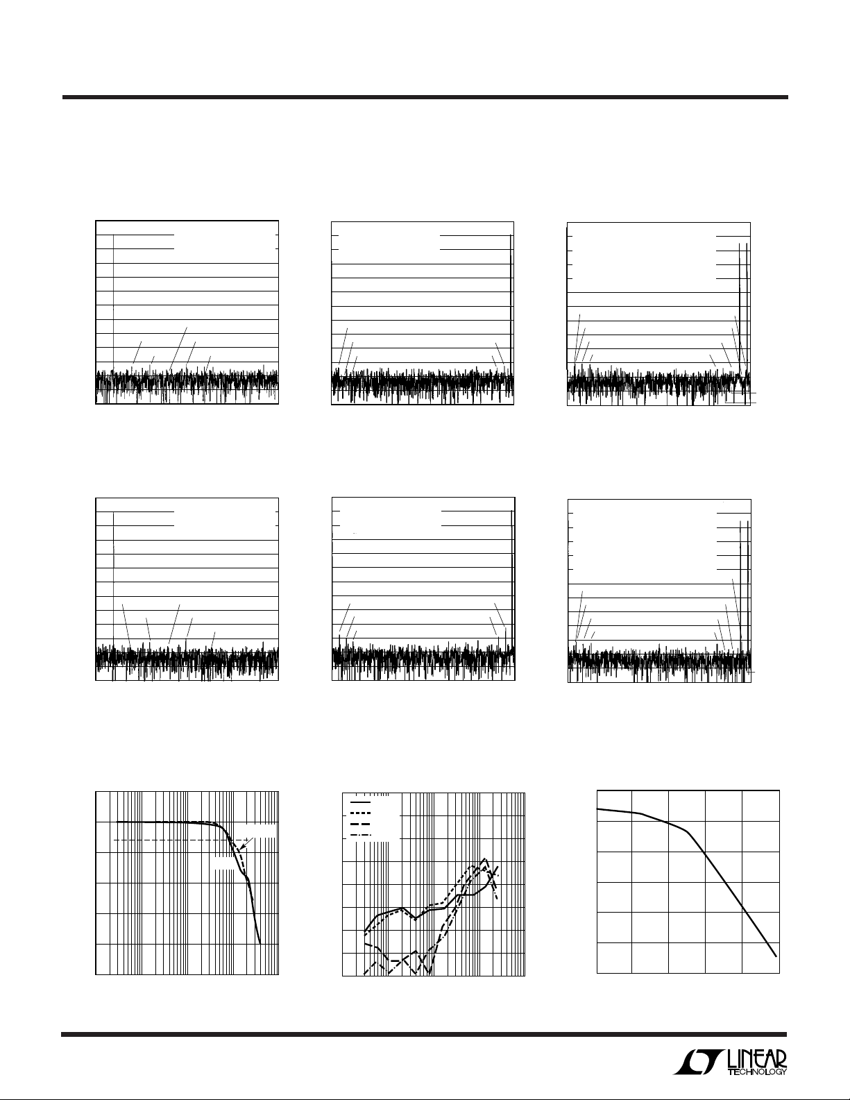
Sine Wave Spectrum Plot
(Bipolar) ±5V Supply
10
0
–10
–20
–30
–40
–50
–60
–70
AMPLITUDE (dB)
–80
–90
–100
–110
–120
0
Sine Wave Spectrum Plot
(Unipolar) 5V Supply
10
0
–10
–20
–30
–40
–50
–60
–70
AMPLITUDE (dB)
–80
–90
–100
–110
–120
2ND
0
4V
Power Bandwidth and
P-P
100mV
P-P
Bandwidth
5
0
–5
–10
AMPLITUDE (dB)
–15
–20
–25
0.1 10 100 1000
6
1
f
SAMPLE
f
= 109592.01Hz
SINE
2048 SAMPLES
4TH
2ND
FREQUENCY (MHz)
3RD
FREQUENCY (MHz)
5TH
3RD
0.55 1.11
f
SAMPLE
= 109592.01Hz
f
SINE
2048 SAMPLES
4TH
5TH
0.55 1.11
Small-Signal
FREQUENCY (MHz)
= 2222222.22Hz
6TH
1402 G09
= 2222222.22Hz
6TH
1402 G12
100mV
P-P
4V
P-P
1402 F07
Sine Wave Spectrum Plot
(Bipolar) Dual ±5V Supply
10
f
= 2222222.22Hz
SAMPLE
0
= 1131727.43Hz
f
SINE
–10
2048 SAMPLES
–20
–30
–40
–50
–60
2ND
–70
AMPLITUDE (dB)
–80
–90
–100
–110
–120
4TH
6TH
0
0.55 1.11
FREQUENCY (MHz)
Sine Wave Spectrum Plot
(Unipolar) 5V Supply
10
f
= 2222222.22Hz
SAMPLE
0
= 1131727.43Hz
f
SINE
–10
2048 SAMPLES
–20
–30
–40
–50
–60
2ND 3RD
–70
AMPLITUDE (dB)
–80
–90
–100
–110
–120
4TH
6TH
0
0.55 1.11
FREQUENCY (MHz)
PSRR vs Frequency
0
–10
–20
–30
–40
–50
REJECTION (dB)
–60
–70
–80
V
CC
V
SS
V
DD
DGND
0.1 10 100 1000
1
FREQUENCY (MHz)
5TH
5TH
3RD
1402 G11
1402 G08
1402 G18
IMD Spectrum Plot (Bipolar)
10
f
= 2352941.18Hz
SAMPLE
0
–10
–20
–30
–40
–50
–60
–70
AMPLITUDE (dB)
–80
–90
–100
–110
–120
= 1250000Hz ±1V INTO A
f
SINEA
f
= 1199449Hz ±1V INTO A
SINEB
IMD = 83.9dB
2048 SAMPLES
– f
f
A
B
2f
B
fA – f
B
2f
A
0
FREQUENCY (MHz)
0.59 1.18
IMD Spectrum Plot (Unipolar)
10
f
= 2352941.18Hz
SAMPLE
0
–10
–20
–30
–40
–50
–60
–70
AMPLITUDE (dB)
–80
–90
–100
–110
–120
= 1250000Hz INTO A
f
SINEA
1.5V TO 3.5V
= 1199449Hz INTO A
f
SINEB
1.5V TO 3.5V
IMD = –84.1dB
2048 SAMPLES
– f
f
A
B
2f
B
fA + f
B
2f
A
0
FREQUENCY (MHz)
2fA – fB, fA + 2f
0.59 1.18
Load Regulation for V
fA + 2f
+
IN
–
IN
2fA + f
3f
,
,
+
IN
–
IN
fA – 2f
A
3f
A
B
B
REF
B
3f
B
2fA – f
B
2fA + f
B
1402 G10
3f
B
B
fA – 2f
B
1402 G13
 Loading...