

Linear Technology LTC1401 Datasheet
FEATURES
LTC1401
Complete
SO-8, 12-Bit, 200ksps
ADC with Shutdown
U
DESCRIPTION
■
Complete 12-Bit ADC with Reference in SO-8
■
Single Supply 3V Operation
■
Sample Rate: 200ksps
■
Power Dissipation: 15mW (Typ)
■
68dB S/(N + D) and – 72dB THD at 50kHz
■
No Missing Codes Over Temperature
■
Nap Mode with Instant Wake-Up: 1.5mW
■
Sleep Mode: 19.5µW
■
Shutdown Mode: 13.5µW
■
High Impedance Analog Input
■
Input Range (0.5mV/LSB): 0V to 2.048V
■
Internal Reference Can Be Overdriven Externally
■
3-Wire Interface to DSPs and Processors (SPI and
MICROWIRETM Compatible)
U
APPLICATIONS
■
Low Power and Battery-Operated Systems
■
Handheld or Portable Instruments
■
High Speed Data Acquisition
■
Digital Signal Processing
■
Multiplexed Data Acquisition Systems
■
Telecommunication
■
Digital Radio
■
Spectrum Analysis
The LTC®1401 is a complete 200ksps, 12-bit A/D converter that converts 0V to 2.048V unipolar input and draws
only 15mW from a single 3V supply. This easy-to-use
device comes complete with a 315ns sample-and-hold
and a precision reference. Maximum DC specifications
include ±1LSB INL, ±1LSB DNL and 45ppm/°C full-scale
drift over temperature.
The LTC1401 has three power saving modes: Nap and
Sleep, through the serial interface and Shutdown by
setting the SHDN pin to zero. In Nap mode, it consumes
only 1.5mW of power and can wake up and convert
immediately. In Sleep (Shutdown) mode, it consumes
19.5µW (13.5µW) of power typically. Upon power-up
from Sleep or Shutdown mode, a reference ready (REFRDY)
signal is available in the serial word to indicate that the
reference has settled and the chip is ready to convert.
The 3-wire serial port allows compact and efficient data
transfer to a wide range of microprocessors, microcontrollers and DSPs.
, LTC and LT are registered trademarks of Linear Technology Corporation.
MICROWIRE is a trademark of National Semiconductor Corporation.
U
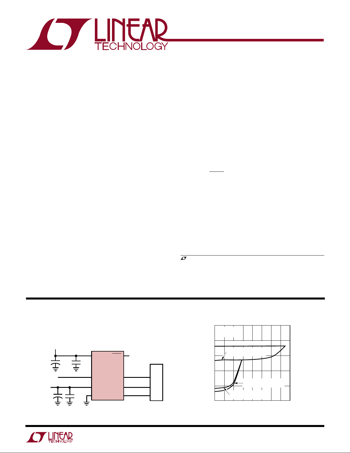
TYPICAL APPLICATION
Single 3V Supply, 200kHz, 12-Bit Sampling A/D Converter
3V
+
ANALOG INPUT
(0V TO 2.048V)
1.20V
1
V
CC
0.1µF10µF
LTC1401
2
A
IN
3
V
+
0.1µF10µF
REF
4
GND
SHDN
CONV
CLK
D
OUT
8
7
6
5
SERIAL
DATA LINK
MPU
P1.4
P1.3
P1.2
1401 TA01
Power Consumption vs Sample Rate
100
3.2MHz CLOCK
= 25°C
T
A
10
1
0.1
SUPPLY CURRENT (mA)
0.01
0.001
0.01
NORMAL CONVERSION
NAP MODE
BETWEEN CONVERSION
SHUTDOWN MODE
BETWEEN CONVERSION
SLEEP MODE BETWEEN
CONVERSION
100
0.1 1
10 1k 1M
SAMPLE RATE (Hz)
10k 100k
LTC1401 • TA02
1
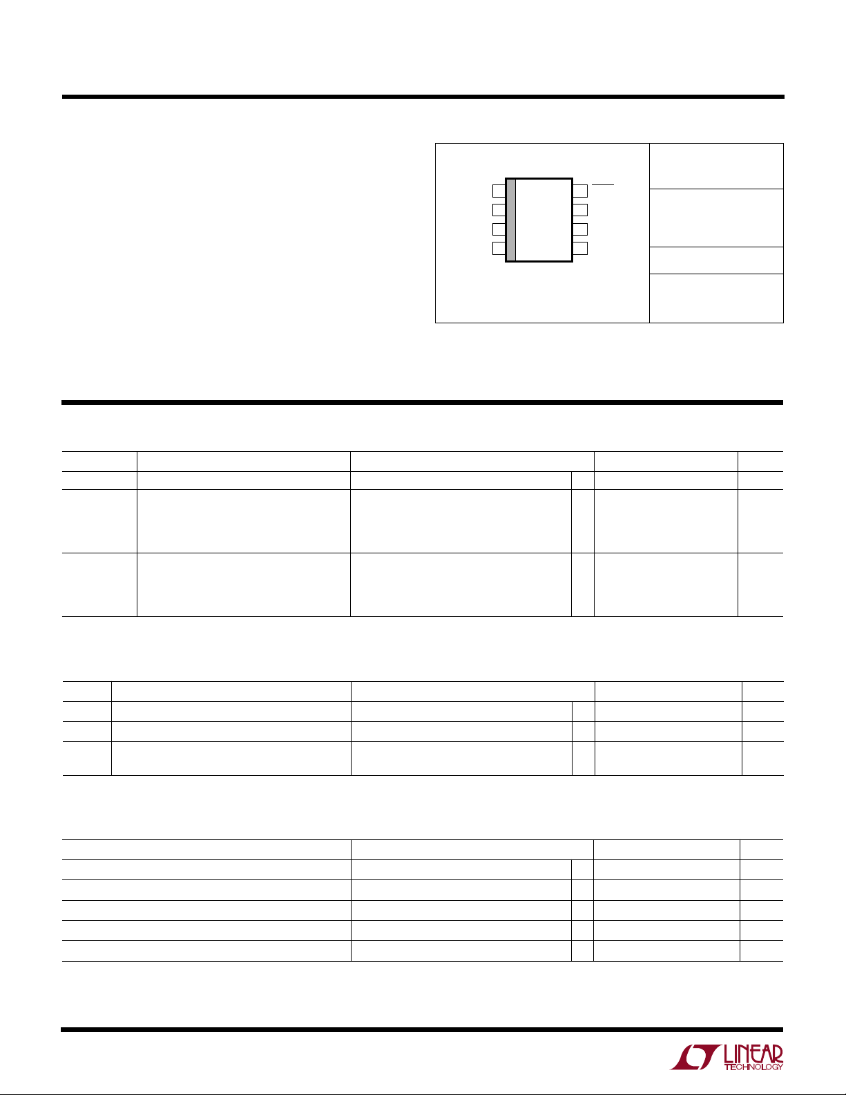
LTC1401
TOP VIEW
V
CC
A
IN
V
REF
GND
SHDN
CONV
CLK
D
OUT
S8 PACKAGE
8-LEAD PLASTIC SO
1
2
3
4
8
7
6
5
WW
W
ABSOLUTE MAXIMUM RATINGS
(Notes 1, 2)
Supply Voltage (VCC) ................................................. 7V
Analog Input Voltage (Note 3) ..... –0.3V to (VCC + 0.3V)
Digital Input Voltage (Note 4) ....................–0.3V to 12V
Digital Output Voltage.................. –0.3V to (VCC + 0.3V)
U
U
W
PACKAGE/ORDER INFORMATION
ORDER PART
NUMBER
LTC1401CS8
LTC1401IS8
Power Dissipation.............................................. 300mW
Operating Ambient Temperature Range
LTC1401C................................................0°C to 70°C
LTC1401I............................................ – 40°C to 85°C
T
= 125°C, θJA = 130°C/ W
JMAX
S8 PART MARKING
1401
1401I
Operating Junction Temperature ......................... 125°C
Storage Temperature Range ................. –65°C to 150°C
Consult factory for PDIP packages and Military grade parts.
Lead Temperature (Soldering, 10 sec)..................300°C
U
W
POWER REQUIRE E TS
SYMBOL PARAMETER CONDITIONS MIN TYP MAX UNITS
V
CC
I
CC
P
D
Supply Voltage 2.7 3.0 3.6 V
Supply Current f
Power Dissipation f
(Note 5)
= 200ksps ● 510 mA
SAMPLE
Nap Mode
Sleep Mode
Shutdown Mode ● 4.5 10 µA
= 200ksps ● 15 30 mW
SAMPLE
Nap Mode
Sleep Mode
Shutdown Mode ● 13.5 30 µW
● 0.5 1.0 mA
● 6.5 15 µA
● 1.5 3.0 mW
● 19.5 45 µW
U
IA
U
PUT
(Note 5)
During Conversions (Hold Mode) 5 pF
(Note 5)
= 0 1.180 1.200 1.220 V
OUT
= 0 ● ±10 ±45 ppm/°C
OUT
≤ 1mA 2 LSB/mA
OUT
= 10µF3ms
VREF
U
IN
U
LOG
IN
IN
Analog Input Range ● 0 to 2.048 V
Analog Input Leakage Current During Conversions (Hold Mode) ● ±1 µA
Analog Input Capacitance Between Conversions (Sample Mode) 45 pF
UU
A
SYMBOL PARAMETER CONDITIONS MIN TYP MAX UNITS
V
I
C
I TER AL REFERE CE CHARACTERISTICS
PARAMETER CONDITIONS MIN TYP MAX UNITS
V
Output Voltage I
REF
V
Output Tempco I
REF
V
Line Regulation 2.7V ≤ VCC ≤ 3.6V 0.01 LSB/V
REF
V
Load Regulation 0 ≤ I
REF
V
Wake-Up Time from Sleep or Shutdown Mode C
REF
2
LTC1401
U
CO
PARAMETER CONDITIONS MIN TYP MAX UNITS
Resolution (No Missing Codes) ● 12 Bits
Integral Linearity Error (Note 7) ● ±1 LSB
Differential Linearity Error ● ±1 LSB
Offset Error ±6 LSB
Full-Scale Error ±15 LSB
Full-Scale Tempco I
DY
SYMBOL PARAMETER CONDITIONS MIN TYP MAX UNITS
S/(N + D) Signal-to-Noise 50kHz Input Signal ● 65 68 dB
THD Total Harmonic Distortion 50kHz Input Signal ● –72 –65 dB
IMD Intermodulation Distortion f
VERTER
W
U
IC
A
Plus Distortion Ratio 100kHz Input Signal 65 dB
Up to 5th Harmonic 100kHz Input Signal –66 dB
Peak Harmonic or 50kHz Input Signal ● –74 –65 dB
Spurious Noise 100kHz Input Signal –67 dB
Full Power Bandwidth 2 MHz
Full Linear Bandwidth (S/(N + D) ≥ 68dB) 50 kHz
CCHARA TERIST
ACCURACY
(Note 5)
ICS
OUT(REF)
IN1
With internal reference (Note 5)
● ±8 LSB
= 0 ● ±10 ±45 ppm/°C
= 49.853kHz, f
= 53.076kHz –69 dB
IN2
UU
DIGITAL I PUTS AND OUTPUTS
SYMBOL PARAMETER CONDITIONS MIN TYP MAX UNITS
V
IH
V
IL
I
IN
C
IN
V
OH
V
OL
I
OZ
C
OZ
I
SOURCE
I
SINK
High Level Input Voltage V
Low Level Input Voltage VCC = 2.7V ● 0.8 V
Digital Input Current VIN = 0V to V
Digital Input Capacitance 5pF
High Level Output Voltage VCC = 2.7V, IO = –10µA ● 2.40 2.64 V
Low Level Output Voltage VCC = 2.7V, IO = 400µA ● 0.13 0.4 V
Hi-Z Output Leakage D
Hi-Z Output Capacitance D
Output Source Current V
Output Sink Current V
OUT
OUT
(Note 5)
= 3.6V ● 2.0 V
CC
CC
VCC = 2.7V, IO = –200µA ● 2.25 2.50 V
V
= 0V to V
OUT
= 0 –5 mA
OUT
= V
OUT
CC
CC
● ±10 µA
● ±10 µA
15 pF
10 mA
3
LTC1401
W
U
TI I G CHARACTERISTICS
SYMBOL PARAMETER CONDITIONS MIN TYP MAX UNITS
f
SAMPLE(MAX)
t
CONV
t
ACQ
f
CLK
t
CLK
t
WK(NAP)
t
1
t
2
t
3
t
4
t
5
t
6
t
7
t
8
t
9
t
10
Maximum Sampling Frequency ● 200 kHz
Conversion Time f
Acquisition Time 315 ns
CLK Frequency ● 0.1 3.2 MHz
CLK Pulse Width (Note 6) ● 60 ns
Time to Wake Up from Nap Mode 350 ns
CLK Pulse Width to Return to Active Mode ● 60 ns
CONV↑ to CLK↑ Setup Time ● 100 ns
CONV↑ After Leading CLK↑ ● 0ns
CONV Pulse Width (Note 8) ● 50 ns
Time from CLK↑ to Sample Mode 80 ns
Aperture Delay of Sample-and-Hold Jitter < 50ps 45 ns
Minimum Delay Between Conversion (Note 6) ● 350 550 ns
Delay Time, CLK↑ to D
Delay Time, CLK↑ to D
Time from Previous Data Remains Valid After CLK↑ C
Valid C
OUT
Hi-Z C
OUT
(Note 5)
= 3.2MHz ● 4.1 µs
CLK
= 20pF ● 60 120 ns
LOAD
= 20pF ● 60 120 ns
LOAD
= 20pF ● 15 50 ns
LOAD
The ● denotes specifications which apply over the full operating
temperature range; all other limits and typicals apply to TA = 25°C.
Note 1: Absolute Maximum Ratings are those values beyond which the life
of a device may be impaired.
Note 2: All voltage values are with respect to GND.
Note 3: When these pin voltages are taken below GND or above V
will be clamped by internal diodes. This product can handle input currents
greater than 40mA without latch-up if the pin is driven below GND or
above VCC.
Note 4: When these pin voltages are taken below GND, they will be clamped
by internal diodes. This product can handle input currents greater than 40mA
without latch-up if the pin is driven below GND. These pins are not clamped
.
to V
CC
CC
, they
Note 5: V
specified.
Note 6: Guaranteed by design, not subject to test.
Note 7: Integral nonlinearity is defined as the deviation of a code from a
straight line passing through the actual endpoints of the transfer curve.
The deviation is measured from the center of the quantization band.
Note 8: The rising edge of CONV starts a conversion. If CONV returns low
at a bit decision point during the conversion, it can create small errors. For
best performance, ensure that CONV returns low either within 120ns after
the conversion starts (i.e., before the first bit decision) or after the 14
clock cycles. (Figure 13 Timing Diagram).
= 3V, f
CC
= 200kHz, tr = tf = 5ns unless otherwise
SAMPLE
4
W
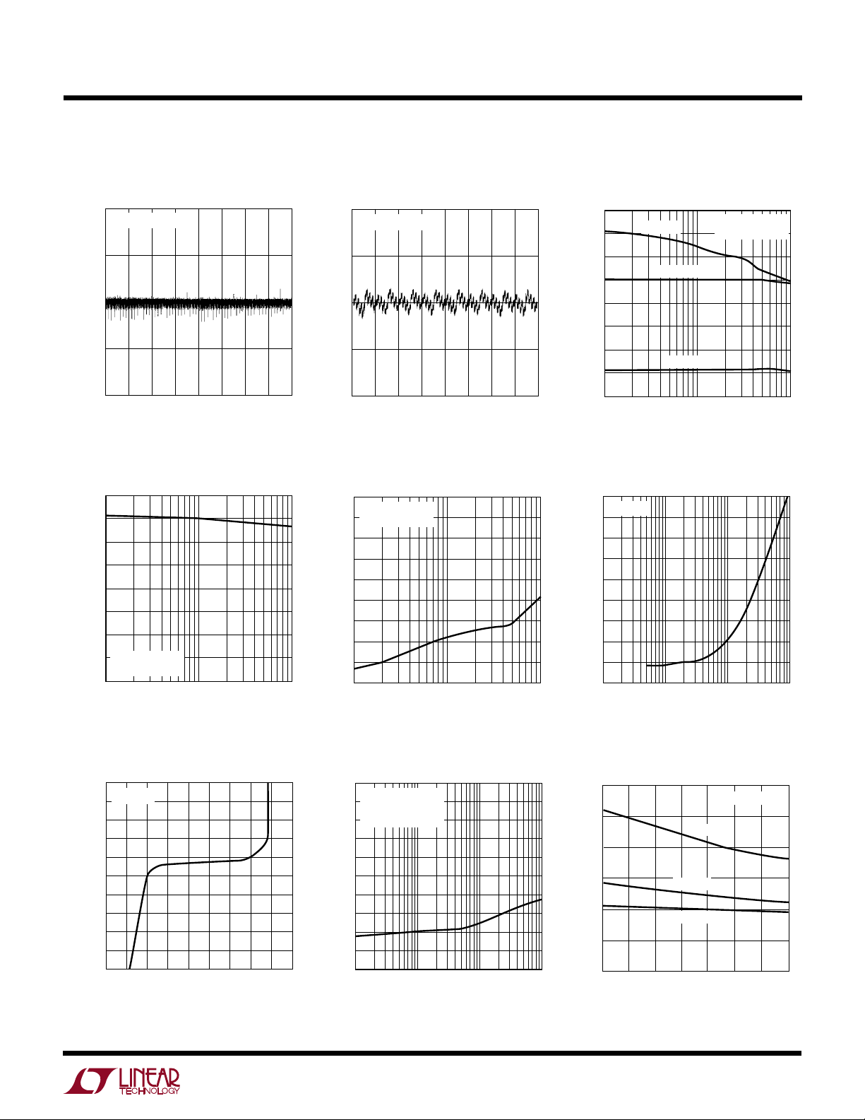
INPUT FREQUENCY (kHz)
10
0
SIGNAL/(NOISE + DISTORTION)(dB)
10
20
30
40
80
100 1000
LTC1401 • TPC03
50
60
70
VIN = 0dB
VIN = –20dB
VIN = –60dB
TA = 25°C
f
SAMPLE
= 200kHz
SOURCE RESISTANCE (Ω)
10
2500
t
ACQ
(ns)
3000
3500
4000
4500
100 1k 10k
LTC1401 • TPC06
2000
1500
500
0
1000
TA = 25°C
U
TYPICAL PERFORMANCE CHARACTERISTICS
LTC1401
Differential Nonlinearity vs
Output Code
1.0
f
= 200kHz
SAMPLE
0.5
0
DNL ERROR (LSBs)
–0.5
–1.0
0
512 1024 1536 2048
2560 3072 3584 4096
CODE
Signal-to-Noise Ratio (Without
Harmonics) vs Input Frequency
80
70
60
50
40
30
20
SIGNAL-TO-NOISE RATIO (dB)
10
TA = 25°C
= 200kHz
f
SAMPLE
0
10
INPUT FREQUENCY (kHz)
100 1000
LTC1401 • TPC01
LTC1401 • TPC04
Integral Nonlinearity vs
Output Code
1.0
f
= 200kHz
SAMPLE
0.5
0
INL ERROR (LSBs)
–0.5
–1.0
0
512 1024 1536 2048
2560 3072 3584 4096
CODE
Peak Harmonic or Spurious Noise
vs Input Frequency
0
TA = 25°C
–10
–20
–30
–40
–50
–60
–70
–80
SPURIOUS-FREE DYNAMIC RANGE (dB)
–90
10
= 200kHz
f
SAMPLE
INPUT FREQUENCY (kHz)
100 1000
S/(N + D) vs Input Frequency
and Amplitude
LTC1401 • TPC02
Acquisition Time vs
Source Impedance
LTC1401 • TPC05
Reference Voltage vs
Load Current
1.40
TA = 25°C
1.35
1.30
1.25
1.20
1.15
1.10
1.05
REFERENCE VOLTAGE (V)
1.00
0.95
0.90
–7
–6 –4
–5
–2 2
–3
LOAD CURRENT (mA)
–1
0
1
LTC1401 • TPC07
Power Supply Feedthrough vs
Ripple Frequency
0
f
= 200kHz
SAMPLE
–10
= 49.853kHz
f
IN
(V
V
–20
CC
–30
–40
–50
–60
–70
–80
POWER SUPPLY FEEDTHROUGH (dB)
–90
–100
1
= 1mV)
RIPPLE
10 100 1000
RIPPLE FREQUENCY (kHz)
LTC1401 • TPC08
Supply Current vs Temperature
12
10
8
6
4
SUPPLY CURRENT (mA)
2
0
–50
–25 0
TEMPERATURE (˚C)
f
SAMPLE
VIN = 3.6V
VIN = 3V
VIN = 2.7V
50 100 125
25 75
= 200kHz
LTC1401 • TPC09
5
LTC1401
PIN FUNCTIONS
UUU
V
(Pin 1): Positive Supply, 3V. Bypass to GND (10µF
CC
tantalum in parallel with 0.1µF ceramic).
AIN (Pin 2): Analog Input. 0V to 2.048V.
V
(Pin 3): 1.2V Reference Output. Bypass to GND
REF
(10µF tantalum in parallel with 0.1µF ceramic).
GND (Pin 4): Ground. GND should be tied directly to an
analog ground plane.
D
(Pin 5): The A/D conversion result is shifted out from
OUT
this pin.
UU
W
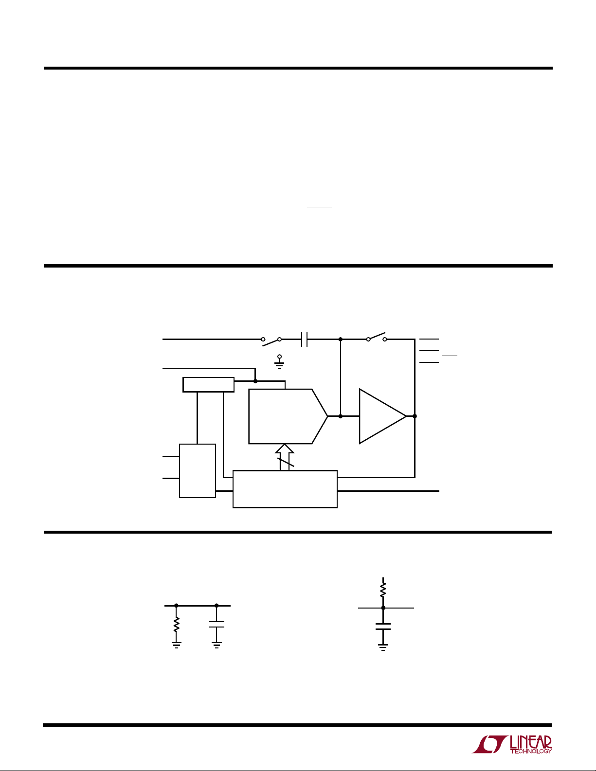
FUNCTIONAL BLOCK DIAGRA
A
IN
V
REF
1.20V REF
CLK (Pin 6): Clock. This clock synchronizes the serial data
transfer. A minimum CLK pulse of 60ns signals the ADC to
wake up from Nap or Sleep mode.
CONV (Pin 7): Conversion Start Signal. This active high
signal starts a conversion on its rising edge. Keeping CLK
low and pulsing CONV two/four times will put the ADC into
Nap/Sleep mode.
SHDN (Pin 8): Shutdown Input. Pull this pin Low to put the
ADC in Shutdown mode and save power (REFRDY will go
Low). The device will draw 4.5µA in this mode.
C
SAMPLE
ZEROING SWITCH
V
CC
GND
SHDN
TEST CIRCUITS
CLK
CONV
D
OUT
CONTROL
LOGIC
3k
Hi-Z TO V
V
OL TO VOH
V
TO Hi-Z
OH
12-BIT CAPACITIVE DAC COMP
12
SUCCESSIVE APPROXIMATION
REGISTER/PARALLEL TO
SERIAL CONVERTER
3V
3k
D
OUT
C
LOAD
OH
Hi-Z TO V
V
OH TO VOL
V
TO Hi-Z
OL
C
LOAD
OL
LTC1401 • TC01
D
OUT
LTC1401 • BD01
6
 Loading...