

FEATURES
ANALOG INPUT VOLTAGE (V)
–5 –4 –2 0 2 4
ON-RESISTANCE (Ω)
300
250
200
150
100
50
0
–3 –1 1 3
1391 TA02
5
TA = 25°C
V+ = 2.7V
V
–
= 0V
V+ = 5V
V
–
= –5V
■
Low RON: 45Ω
■
Single 2.7V to ±5V Supply Operation
■
Analog Inputs May Extend to Supply Rails
■
Low Charge Injection
■
Serial Digital Interface
■
Low Leakage: ±5nA Max
■
Guaranteed Break-Before-Make
■
TTL/CMOS Compatible for All Digital Inputs
■
Cascadable to Allow Additional Channels
■
Can Be Used as a Demultiplexer
U
APPLICATIONS
■
Data Acquisition Systems
■
Communication Systems
■
Signal Multiplexing/Demultiplexing
LTC1391
8-Channel
Analog Multiplexer with
Cascadable Serial Interface
U
DESCRIPTION
The LTC®1391 is a high performance CMOS 8-to-1 analog
multiplexer. It features a serial digital interface that allows
several LTC1391s to be daisy-chained together, increasing the number of MUX channels available using a single
digital port.
The LTC1391 features a typical RON of 45Ω, a typical
switch leakage of 50pA and guaranteed break-beforemake operation. Charge injection is ±10pC maximum. All
digital inputs are TTL and CMOS compatible when operated from single or dual supplies. The inputs can withstand 100mA fault current.
The LTC1391 is available in 16-pin PDIP, SSOP and
narrow SO packages. For applications requiring 2-way
serial data transmission, see the LTC1390 data sheet.
, LTC and LT are registered trademarks of Linear Technology Corporation.
U
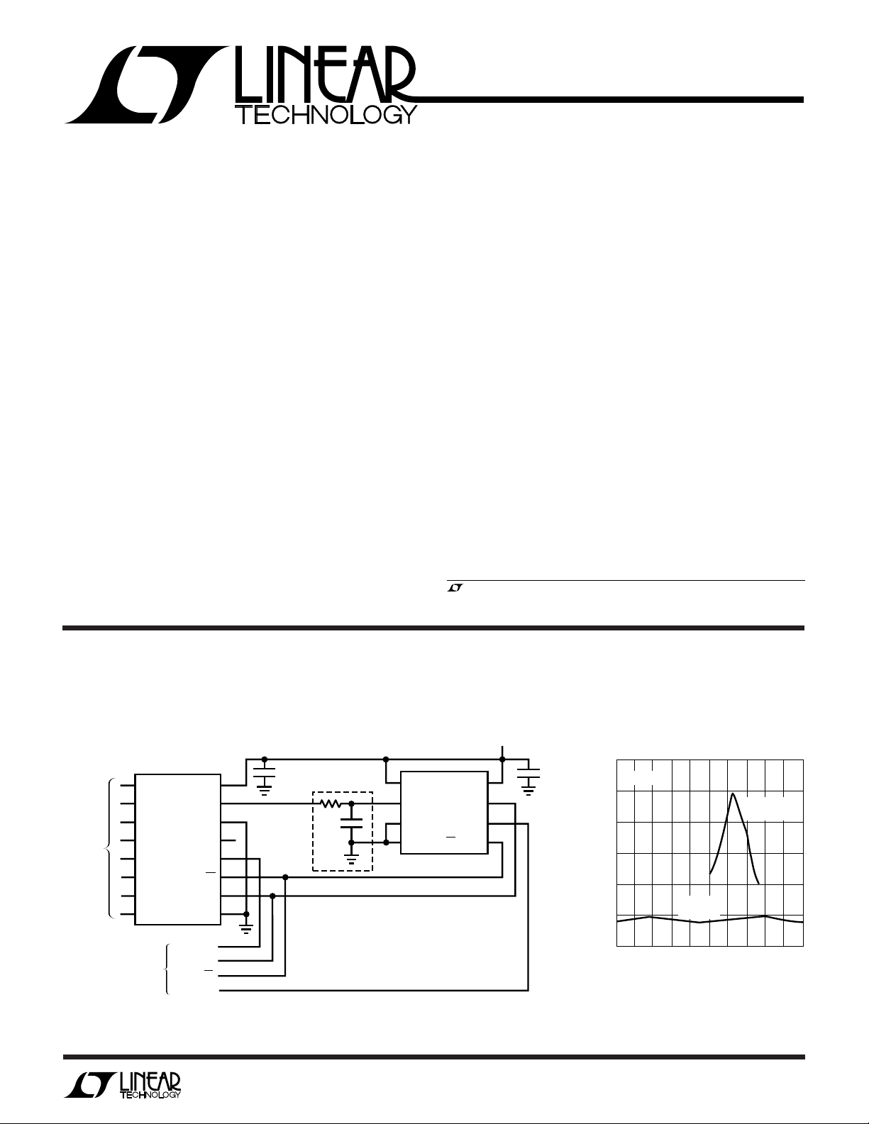
TYPICAL APPLICATION
On-Resistance vs
3V, 8-Channel 12-Bit ADC
OPTIONAL A/D
0.1µF
INPUT FILTER
D
GND
CLK
OUT
D
CLK
CS
16
+
V
15
D
14
–
V
13
12
IN
11
CS
10
9
1
S0
2
S1
3
S2
4
ANALOG
INPUTS
SERIAL INTERFACE
TO MUX AND ADC
5
6
7
8
S3
S4
S5
S6
S7
LTC1391
DATA IN
DATA OUT
1
V
REF
2
+IN
LTC1285
3
–IN
4
GND
CS/SHDN
3V
8
V
CC
7
CLK
6
D
OUT
5
1µF
1391 TA01
Analog Input Voltage
1
LTC1391
WW
W
ABSOLUTE MAXIMUM RATINGS
U
PACKAGE/ORDER INFORMATION
(Note 1)
Total Supply Voltage (V+ to V–) .............................. 15V
Input Voltage
Analog Inputs ................... (V– – 0.3V) to (V+ + 0.3V)
Digital Inputs .........................................–0.3V to 15V
Digital Outputs ..........................–0.3V to (V+ + 0.3V)
Power Dissipation.............................................. 500mW
Operating Temperature Range
LTC1391C ............................................... 0°C to 70°C
LTC1391I........................................... –40°C to 85°C
Storage Temperature Range ................. – 65°C to 150°C
Lead Temperature (Soldering, 10 sec).................. 300°C
S0
S1
S2
S3
S4
S5
S6
S7
GN PACKAGE
16-LEAD PLASTIC SSOP
T
JMAX
T
JMAX
T
JMAX
Consult factory for Military grade parts.
TOP VIEW
1
2
3
4
5
6
7
8
S PACKAGE
16-LEAD PLASTIC SO
= 125°C, θJA = 110°C/ W (GN)
= 125°C, θJA = 70°C/ W (N)
= 125°C, θJA = 100°C/ W (S)
ELECTRICAL CHARACTERISTICS
V+ = 5V, V– = –5V, GND = 0V, TA = operating temperature range, unless otherwise specified.
16
15
14
13
12
11
10
9
N PACKAGE
16-LEAD PDIP
+
V
D
–
V
D
OUT
DIN
CS
CLK
GND
U
W
ORDER PART
NUMBER
LTC1391CGN
LTC1391CN
LTC1391CS
LTC1391IGN
LTC1391IN
LTC1391IS
GN PART MARKING
1391
1391I
U
SYMBOL PARAMETER CONDITIONS MIN TYP MAX UNITS
Switch
V
ANALOG
R
ON
I
S(OFF)
I
D(OFF)
I
D(ON)
Digital
V
INH
V
INL
I
INL
V
OH
V
OL
Dynamic
f
CLK
t
ON
t
OFF
t
OPEN
OIRR Off Isolation VS = 2V
Q
INJ
Analog Signal Range (Note 2) ● –5 5 V
On-Resistance VS = ±3.5V T
ID = 1mA 25°C4575Ω
∆RON vs V
∆RON vs Temperature 0.5 %/°C
Off Input Leakage VS = 4V, VD = –4V, VS = –4V, VD = 4V ±0.05 ±5nA
Off Output Leakage VS = 4V, VD = –4V, VS = –4V, VD = 4V ±0.05 ±5nA
On Channel Leakage VS = VD = ±4V ±0.05 ±5nA
High Level Input Voltage V+ = 5.25V ● 2.4 V
Low Level Input Voltage V+ = 4.75V ● 0.8 V
, I
Input Current VIN = 5V, 0V ● ±5 µA
INH
High Level Output Voltage V+ = 4.75V, IO = –10µA 4.74 V
Low Level Output Voltage V+ = 4.75V, IO = 1.6mA ● 0.5 0.8 V
Clock Frequency (Note 2) 5 MHz
Enable Turn-On Time VS = 2.5V, RL = 1k, CL = 35pF 260 400 ns
Enable Turn-Off Time VS = 2.5V, RL = 1k, CL = 35pF 100 200 ns
Break-Before-Make Interval 35 155 ns
Charge Injection RS = 0, CL = 1000pF, VS = 1V (Note 2) ±2 ±10 pC
S
Channel Off ● ±20 nA
Channel Off ● ±20 nA
Channel On ● ±20 nA
IO = –360µA ● 2.4 4.50 V
, RL = 1k, f = 100kHz 70 dB
P–P
T
MIN
MAX
20 %
75 Ω
120 Ω
2
LTC1391
ELECTRICAL CHARACTERISTICS
V+ = 5V, V– = –5V, GND = 0V, TA = operating temperature range, unless otherwise specified.
SYMBOL PARAMETER CONDITIONS MIN TYP MAX UNITS
Dynamic
C
S(OFF)
C
D(0FF)
Supply
+
I
–
I
V+ = 2.7V, V– = GND = 0V, TA = operating temperature range, unless otherwise specified.
SYMBOL PARAMETER CONDITIONS MIN TYP MAX UNITS
Switch
V
ANALOG
R
ON
I
S(OFF)
I
D(OFF)
I
D(ON)
Digital
V
INH
V
INL
I
INL
V
OH
V
OL
Dynamic
f
CLK
t
ON
t
OFF
t
OPEN
QIRR Off Isolation VS = 2V
Q
INJ
C
S(OFF)
C
D(OFF)
Supply
+
I
Input Off Capacitance 5pF
Output Off Capacitance 10 pF
Positive Supply Current All Logic Inputs Tied Together, VIN = 0V or 5V ● 15 40 µA
Negative Supply Current All Logic Inputs Tied Together, VIN = 0V or 5V ● –15 –40 µA
Analog Signal Range (Note 2) ● 0 2.7 V
On-Resistance VS = 1.2V T
MIN
300 Ω
IO = 1mA 25°C 250 300 Ω
∆RON vs V
T
MAX
S
20 %
350 Ω
∆RON vs Temperature 0.5 %/°C
Off Input Leakage VS = 2.5V, VD = 0.5V; VS = 0.5V, VD = 2.5V (Note 3) ±0.05 ±5nA
Channel Off ● ±20 nA
Off Output Leakage VS = 2.5V, VD = 0.5V; VS = 0.5V, VD = 2.5V (Note 3) ±0.05 ±5nA
Channel Off ● ±20 nA
On Channel Leakage VS = VD = 0.5V, 2.5V (Note 3) ±0.05 ±5nA
Channel On ● ±20 nA
High Level Input Voltage V+ = 3.0V ● 2.0 V
Low Level Input Voltage V+ = 2.4V ● 0.8 V
, I
Input Current VIN = 2.7V, 0V ● ±5 µA
INH
High Level Output Voltage V+ = 2.7V, IO = –20µA 2.68 V
IO = –400µA ● 2.0 2.30 V
Low Level Output Voltage V+ = 2.7V, IO = 20µA 0.01 V
IO = 400µA ● 0.20 0.8 V
Clock Frequency (Note 2) 5 MHz
Enable Turn-On Time VS = 1.5V, RL = 1k, CL = 35pF (Note 4) 490 800 ns
Enable Turn-Off Time VS = 1.5V, RL = 1k, CL = 35pF (Note 4) 190 400 ns
Break-Before-Make Interval (Note 4) 125 290 ns
, RL = 1k, f = 100kHz 70 dB
P–P
Charge Injection RS = 0, CL = 1000pF, VS = 1V (Note 2) ±1 ±5pC
Input Off Capacitance 5pF
Output Off Capacitance 10 pF
Positive Supply Current All Logic Inputs Tied Together, VIN = 0V or 2.7V ● 0.2 2 µA
The ● denotes specifications which apply over the full operating
temperature range.
Note 1: Absolute Maximum Ratings are those values beyond which the life
of a device may be impaired.
Note 2: Guaranteed by Design.
Note 3: Leakage current with a single 2.7V supply is guaranteed by
correlation with the ±5V leakage current specifications.
Note 4: Timing specifications with a single 2.7V supply are guaranteed by
correlation with the ±5V timing specifications.
3

LTC1391
TEMPERATURE (°C)
–40
OUTPUT VOLTAGE (V)
0.65
0.60
0.55
0.50
0.45
0.40
0.35
0.30
0.25
0.20
0.15
0.10
60
1391 G03
–20
020
40
80
V+ = 5V
V
–
= –5V
I
O
= 1.8mA
V+ = 2.7V
V
–
= 0V
I
O
= 400µA
UW
TYPICAL PERFORMANCE CHARACTERISTICS
On-Resistance vs Temperature
300
V+ = 2.7V
–
= 0V
250
200
150
100
ON-RESISTANCE (Ω)
50
0
–40 –20
V
= 1.2V
V
S
V+ = 5V
–
= –5V
V
= 0V
V
S
20 40 60
0
TEMPERATURE (°C)
Driver Output High Voltage
vs Output Current
0
–0.5
–1.0
–1.5
–2.0
–2.5
OUTPUT CURRENT (mA)
–3.0
–3.5
–4.0
2.0 2.5
80
1391 G01
V+ = 2.7V
–
= 0V
V
V+ = 5V
–
V
3.0 4.03.5
OUTPUT VOLTAGE (V)
OUTPUT VOLTAGE (V)
= –5V
Driver Output Low Voltage
vs Output Current
1.2
TA = 25°C
1.1
1.0
0.9
0.8
0.7
0.6
0.5
0.4
0.3
0.2
0.1
0
0.2 0.6
0
TA =25°C
4.5
1391 G04
0.4
OUTPUT CURRENT (mA)
5.0
V+ = 2.7V
1.0 2.01.8
1.2
0.8
–
= 0V
V
V+ = 5V
–
V
= –5V
1.4
1.6
1391 G02
Driver Output High Voltage
vs Temperature
5.0
4.5
4.0
3.5
3.0
2.5
2.0
1.5
OUTPUT VOLTAGE (V)
1.0
0.5
0
–40
–20
Driver Output Low Voltage
vs Temperature
V+ = 5V
–
= –5V
V
= 1.6mA
I
O
V+ = 2.7V
–
= 0V
V
= 400µA
I
O
020
TEMPERATURE (°C)
40
60
80
1391 G05
PIN FUNCTIONS
S0, S1, S2, S3, S4, S5, S6, S7 (Pins 1, 2, 3, 4, 5, 6, 7,
8): Analog Multiplexer Inputs.
GND (Pin 9): Digital Ground. Connect to system ground.
CLK (Pin 10): System Clock (TTL/CMOS Compatible). The
clock synchronizes the channel selection bits and the
serial data transfer from DIN to D
CS (Pin 11): Channel Select Input (TTL/CMOS Compatible). A logic high on this input enables the LTC1391 to
read in the channel selection bits and allows digital data
transfer from DIN to D
4
UUU
D
into three-state and enables the selected channel for
OUT
analog signal transmission.
DIN (Pin 12): Digital Input (TTL/CMOS Compatible). Input
for the channel selection bits.
D
(Pin 13): Digital Output (TTL/CMOS Compatible).
OUT
.
OUT
. A logic low on this input puts
OUT
Output from the internal shift register.
V– (Pin 14): Negative Supply.
D (Pin 15): Analog Multiplexer Output.
V+ (Pin 16): Positive Supply.

LTC1391
U
WUU
APPLICATIONS INFORMATION
Multiplexer Operation
Figure 1 shows the block diagram of the components
within the LTC1391 required for MUX operation. The
LTC1391 uses DIN to select the active channel and the chip
select input, CS, to switch on the selected channel as
shown in Figure 2.
When CS is high, the input data on the DIN pin is latched
into the 4-bit shift register on the rising clock edge. The
input data consists of the “EN” bit and a string of three bits
for channel selection. If “EN” bit is logic high as illustrated
in the first input data sequence, it enables the selected
channel. After the clocking in of the last channel selection
bit B0, the CS pin must be pulled low before the next rising
clock edge to ensure correct operation. Once CS is pulled
low, the previously selected channel is switched off to
ensure a break-before-make interval. After a delay of tON,
the selected channel is switched on allowing signal transmission. The selected channel remains on until the next
falling edge of CS. After a delay of t
terminates the analog signal transmission and allows the
CLK
D
IN
CS
CONTROL
LOGIC
4-BIT SHIFT
REGISTER
, the LTC1391
OFF
selection of next channel. If the “EN” bit is logic low, as
illustrated in the second data sequence, it disables all
channels and there will be no analog signal transmission.
Table 1 shows the various bit combinations for channel
selection.
Table 1. Logic Table for Channel Selection
ACTIVE CHANNEL EN B2 B1 BO
All Off 0 X X X
S0 1 0 0 0
S1 1 0 0 1
S2 1 0 1 0
S3 1 0 1 1
S4 1 1 0 0
S5 1 1 0 1
S6 1 1 1 0
S7 1 1 1 1
Digital Data Transfer Operation
The block diagram of Figure 3 shows the components
within the LTC1391 required for serial data transfer. When
CS is held high, data is fed into the 4-bit shift register and
then shifted to D
. Data appears at D
OUT
after the fourth
OUT
rising edge of the clock as shown in Figure 4. The last four
ANALOG INPUTS
(S0 TO S7)
MUX
BLOCK
ANALOG
OUTPUT (D)
1391 • F01
Figure 1. Simplified Block Diagram of the MUX Operation
CLK
CS
D
ANY ANALOG
INPUT
IN
D
EN
HIGH
B2
t
ON
Figure 2. Multiplexer Operation
CLK
D
CS
IN
CONTROL
LOGIC
4-BIT SHIFT
REGISTER
Figure 3. Simplified Block Diagram of the
Digital Data Transfer Operation
EN LO
B2 B1 B0B1 B0
t
OFF
D
OUT
1391 F03
1391 • F02
5

LTC1391
U
WUU
APPLICATIONS INFORMATION
bits clocked into the LTC1391 shift register before CS is
taken low select the MUX channel that is turned on. This
allows a series of devices, with the D
connected to the DIN of the next device, to be programmed
with a single data stream.
D
CLK
D
OUT
IN
1234
D3 D4 D5
D2D1
D2D1
Figure 4. Digital Data Transfer Operation
Multiplexer Expansion
Several LTC1391s can be daisy-chained to expand the
number of multiplexer inputs. No additional interface
ports are required for the expansion. Figure 5 shows two
LTC1391s connected at their analog outputs to form a
16-to-1 multiplexer at the input to an LTC1400 A/D converter.
of one device
OUT
D3 D4 D5
1391 • F04
To ensure that only one channel is switched on at any one
time, two sets of channel selection bits are needed for
DATA as shown in Figure 6. The first data sequence is used
to switch off one MUX and the second data sequence is
used to select one channel from the other MUX or
vice versa. In other words, if bit “ENA” is high and bit
“ENB” is low, one channel of MUX A is switched on and all
channels of MUX B are switched off. If bit “ENA” is low and
bit “ENB” is high, all channels at MUX A are switched off
and one channel of MUX B is switched on. Care should be
taken to ensure that only one LTC1391 is enabled at any
one time to prevent two channels from being enabled
simultaneously.
CLK
D
CS
IN
12345678
ENA A2 A1 A0 ENB
B2 B1 B0
Figure 6. Data Sequence for MUX Expansion
1391 • F06
ANALOG
INPUTS
ANALOG
INPUTS
5V
0.1µF
1
S0
2
S1
3
S2
4
S3
LTC1391
5
S4
S5
S6
S7
S0
S1
S2
S3
S4
S5
S6
S7
A
LTC1391
B
6
7
8
1
2
3
4
5
6
7
8
D
GND
D
GND
OUT
D
CLK
OUT
D
CLK
16
+
V
15
D
14
–
V
13
12
IN
11
CS
10
9
16
+
V
15
D
14
–
V
13
12
IN
11
CS
10
9
–5V
0.1µF
OPTIONAL A/D
INPUT FILTER
+
0.1µF
1
V
CC
2
A
IN
LTC1400
3
V
+
10µF
0.1µF
REF
4
GND
V
CONV
CLK
D
OUT
8
SS
7
6
5
10µF
+
5V
10µF
–5V
0.1µF
DATA
OUT
DATA IN
CS
CLK
1391 • F05
Figure 5. Daisy-Chaining Two LTC1391s for Expansion
6

U
TYPICAL APPLICATIONS
LTC1391
Daisy-Chaining Five LTC1391s
ANALOG
INPUTS
ANALOG
INPUTS
ANALOG
INPUTS
0.1µF BYPASS CAPACITORS FROM
+
TO GND FOR EACH LTC1391
V
1
S0
2
S1
3
S2
LTC1391
4
S3
S4
S5
S6
S7
S0
S1
S2
S3
S4
S5
S6
S7
S0
S1
S2
S3
S4
S5
S6
S7
A
LTC1391
B
LTC1391
C
5
6
7
8
1
2
3
4
5
6
7
8
1
2
3
4
5
6
7
8
D
GND
D
GND
D
GND
V
V
OUT
D
CS
CLK
V
V
OUT
D
CS
CLK
V
V
OUT
D
CS
CLK
16
+
15
D
14
–
13
12
IN
11
10
9
16
+
15
D
14
–
13
12
IN
11
10
9
16
+
15
D
14
–
13
12
IN
11
10
9
5V
1
V
REF
2
+IN
LTC1286
3
–IN
4
GND
D
V
CLK
OUT
CS
8
CC
7
6
5
0.1µF
DATA
OUT
ANALOG
INPUTS
ANALOG
INPUTS
1
S0
2
S1
3
S2
LTC1391
4
S3
5
6
7
8
1
2
3
4
5
6
7
8
D
S4
S5
S6
S7
S0
S1
S2
LTC1391
S3
E
S4
S5
S6
S7
Information furnished by Linear Technology Corporation is believed to be accurate and reliable.
However, no responsibility is assumed for its use. Linear Technology Corporation makes no representation that the interconnection of its circuits as described herein will not infringe on existing patent rights.
D
GND
D
GND
V
V
OUT
D
CS
CLK
V
V
OUT
D
CS
CLK
16
+
15
D
14
–
13
12
IN
11
10
9
16
+
15
D
14
–
13
12
IN
11
10
9
DATA IN
CS
CLK
1391 TA04
7

LTC1391
PACKAGE DESCRIPTION
0.015
0.007 – 0.0098
(0.178 – 0.249)
0.016 – 0.050
(0.406 – 1.270)
* DIMENSION DOES NOT INCLUDE MOLD FLASH. MOLD FLASH
SHALL NOT EXCEED 0.006" (0.152mm) PER SIDE
** DIMENSION DOES NOT INCLUDE INTERLEAD FLASH. INTERLEAD
FLASH SHALL NOT EXCEED 0.010" (0.254mm) PER SIDE
(0.38 ± 0.10)
0° – 8° TYP
U
Dimensions in inches (millimeters) unless otherwise noted.
GN Package
16-Lead Plastic SSOP (Narrow 0.150)
(LTC DWG # 05-08-1641)
0.189 – 0.196*
(4.801 – 4.978)
± 0.004
× 45°
0.053 – 0.068
(1.351 – 1.727)
0.008 – 0.012
(0.203 – 0.305)
N Package
16-Lead PDIP (Narrow 0.300)
(LTC DWG # 05-08-1510)
0.0250
(0.635)
BSC
0.004 – 0.0098
(0.102 – 0.249)
0.229 – 0.244
(5.817 – 6.198)
16
15
12
14
12 11 10
13
5
4
3
678
9
0.150 – 0.157**
(3.810 – 3.988)
GN16 (SSOP) 1098
0.009
(0.229)
REF
0.300 – 0.325
(7.620 – 8.255)
0.015
(0.381)
0.009 – 0.015
(0.229 – 0.381)
+0.025
0.325
–0.015
+0.635
8.255
()
–0.381
*THESE DIMENSIONS DO NOT INCLUDE MOLD FLASH OR PROTRUSIONS.
MOLD FLASH OR PROTRUSIONS SHALL NOT EXCEED 0.010 INCH (0.254mm)
0.010 – 0.020
(0.254 – 0.508)
0.008 – 0.010
(0.203 – 0.254)
*
DIMENSION DOES NOT INCLUDE MOLD FLASH. MOLD FLASH
SHALL NOT EXCEED 0.006" (0.152mm) PER SIDE
**
DIMENSION DOES NOT INCLUDE INTERLEAD FLASH. INTERLEAD
FLASH SHALL NOT EXCEED 0.010" (0.254mm) PER SIDE
× 45°
0.016 – 0.050
0.406 – 1.270
MIN
0° – 8° TYP
0.053 – 0.069
(1.346 – 1.752)
0.130 ± 0.005
(3.302 ± 0.127)
0.125
(3.175)
MIN
0.014 – 0.019
(0.355 – 0.483)
0.045 – 0.065
(1.143 – 1.651)
0.255 ± 0.015*
0.065
(6.477 ± 0.381)
(1.651)
TYP
0.005
(0.127)
MIN
0.100 ± 0.010
(2.540 ± 0.254)
0.018 ± 0.003
(0.457 ± 0.076)
S Package
16-Lead Plastic Small Outline (Narrow 0.150)
(LTC DWG # 05-08-1610)
0.004 – 0.010
(0.101 – 0.254)
0.228 – 0.244
0.050
(1.270)
TYP
(5.791 – 6.197)
0.770*
(19.558)
MAX
910
8
7
N16 0695
11
10
9
0.150 – 0.157**
(3.810 – 3.988)
7
6
8
S16 0695
3
(9.804 – 10.008)
14
3
12
13
4
5
0.386 – 0.394*
13
12
5
4
11
6
14
15
16
2
1
16
15
2
1
8

TYPICAL APPLICATION
Interfacing LTC1391 with LTC1257 for Demultiplex Operation
LTC1391
U
ANALOG
OUTPUTS
TTL COMPATIBLE
+
AT V
= 5V
RELATED PARTS
D
CLK
GND
DATA
CLK
V
OUT
D
CS
CS
16
+
V
15
D
14
–
13
12
IN
11
10
9
47k
OPTIONAL D/A
OUTPUT FILTER
1
CLK
2
D
IN
LTC1257
3
LOAD
4
D
OUT
V
V
GND
V
OUT
REF
8
CC
7
6
5
0.1µF
0.1µF
1391 TA03
5V ≤ V+ ≤ 12V
1
S0
2
S1
3
S2
4
S3
LTC1391
5
S4
6
S5
7
S6
8
S7
PART NUMBER DESCRIPTION COMMENTS
LTC1285 3V 12-Bit ADC Micropower, Auto Shutdown, SO-8 Package, SPI, QSPI + MICROWIRE
TM
Compatible
LTC1286 5V 12-Bit ADC Micropower, Auto Shutdown, SO-8 Package, SPI, QSPI + MICROWIRE Compatible
LTC1390 Serial-Controlled 8-to-1 Analog Multiplexer Low RON, Bidirectional Serial Interface, Low Power, 16-Pin SO
LTC1451 5V 12-Bit DAC Complete V
LTC1452 5V and 3V 12-Bit DAC Multiplying V
LTC1453 3V 12-Bit DAC Complete V
MICROWIRE is a trademark of National Semiconductor.
DAC, SO-8 Package, Daisy-Chainable, Low Power
OUT
DAC, SO-8 Package, Rail-to-Rail Output, Low Power
OUT
DAC, SO-8 Package, Daisy-Chainable, Low Power
OUT
9
Linear Technology Corporation
1630 McCarthy Blvd., Milpitas, CA 95035-7417
(408) 432-1900
●
FAX
: (408) 434-0507
●
TELEX
: 499-3977
1391f, sn1391 LT/GP 0896 7K • PRINTED IN USA
LINEAR TECHNOLOGY CORPORATION 1995
9
 Loading...