

Linear Technology LTC1387 Datasheet
L TC1387
Single 5V RS232/RS485
Multiprotocol Transceiver
EATU
F
■
Two RS232 Transceivers or One RS485 Transceiver
■
Operates from a Single 5V Supply
■
Guaranteed Receiver Output with Inputs
RE
S
Floating or Shorted to Ground
■
Logic Selectable Fast/Slow RS485 Driver Slew Rate
■
Low Supply Current: 7mA Typical
■
5µA Supply Current in Shutdown
■
Self-Testing Capability in Loopback Mode
■
Separate Driver and Receiver Enable Controls
■
Driver Maintains High Impedance in Three-State,
Shutdown or with Power Off
■
Receiver Inputs Can Withstand ±25V
U
APPLICATIONS
■
Point-of-Sale Terminals
■
Software Selectable Multiprotocol Interface Ports
■
Low Power RS485/RS422/RS232/EIA562 Interface
■
Cable Repeaters
■
Level Translators
DUESCRIPTIO
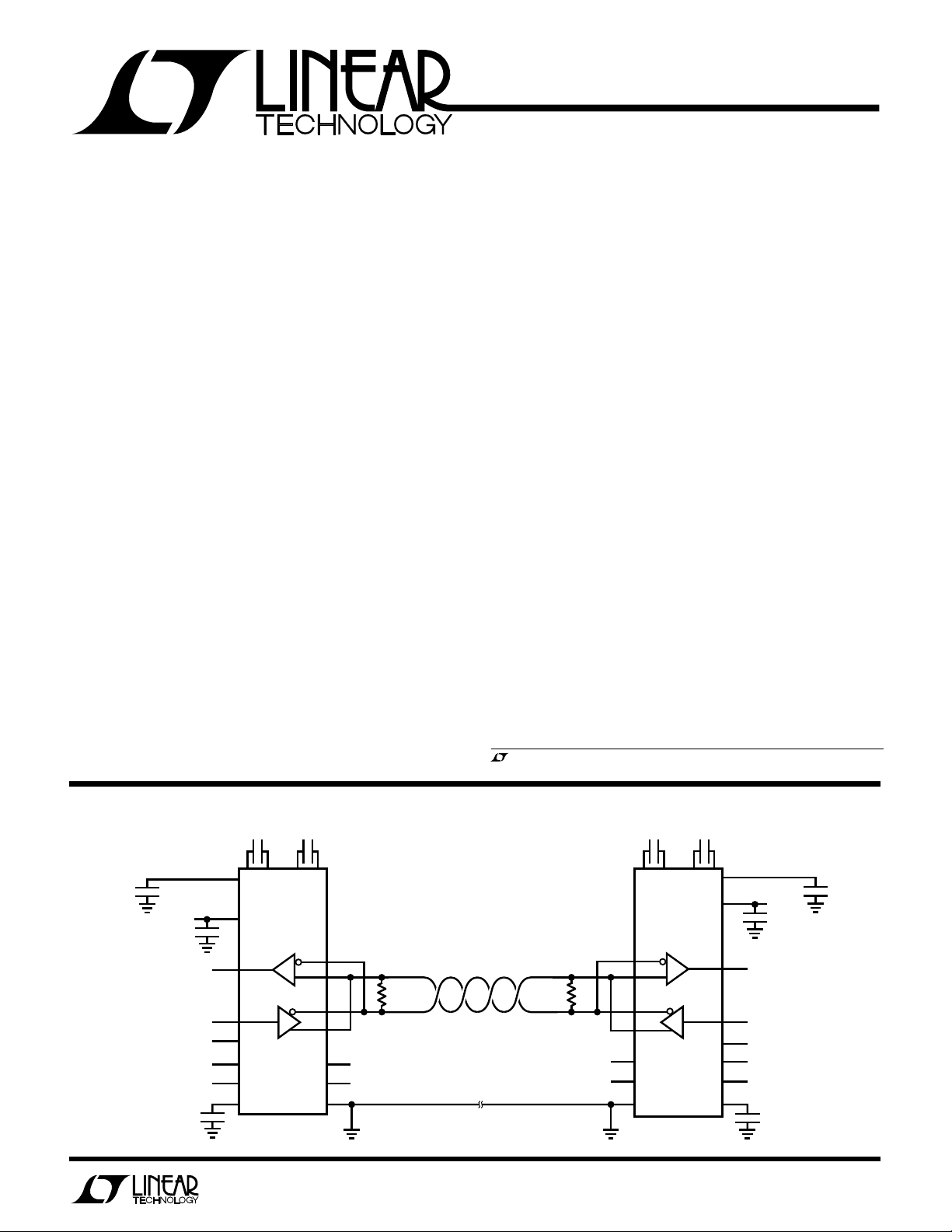
The LTC®1387 is a low power reconfigurable CMOS bidirectional transceiver. It can be configured as an RS485
differential port or as two RS232 single-ended ports. An
onboard charge pump uses four 0.1µF capacitors to
generate boosted positive and negative supplies, allowing
the RS232 drivers to meet ±5V output swing requirements with only a single 5V supply. A shutdown mode
reduces the ICC supply current to 5µA.
The RS232 transceivers are in full compliance with RS232
specification. The RS485 transceiver is in full compliance
with RS485 and RS422 specifications. The RS485 receiver assumes a known output state when the inputs are
floating or shorted to ground. All interface drivers feature
short-circuit and thermal shutdown protection. An enable
pin allows RS485 driver outputs to be forced into high
impedance which is maintained even when the outputs are
forced beyond supply rails or the power is off. A loop back
mode allows the driver outputs to be connected back to the
receiver inputs for diagnostic self-test.
The LTC1387 is available in 20-pin plastic SSOP and SW
packages.
, LTC and LT are registered trademarks of Linear Technology Corporation.
A
PPLICATITYPICAL
V
CC1
5V
RECOUT
DR IN
SLEW
DR ENABLE
U
O
12
3
LTC1387
18
17
15
14
9
12
5V
11
1920
4
5
6
7
8
13
10
120Ω
5V
5V
ALL CAPACITORS: 0.1µF MONOLITHIC CERAMIC TYPE
RS485 INTERFACE
4000-FT 24-GAUGE TWISTED PAIR
120Ω
LTC1387
4
5
6
7
8
5V
13
5V
10
212019
3
18
17
15
14
9
12
11
V
CC2
5V
RECOUT
DR IN
SLEW
DR ENABLE
5V
LTC1387 • TA01
1
LTC1387
WU
U
PACKAGE
/
O
RDER I FOR ATIO
A
W
O
LUTEXI T
S
A
WUW
ARB
U
G
I
S
(Note 1)
Supply Voltage (VCC) ............................................. 6.5V
Input Voltage
Drivers ................................... –0.3V to (VCC + 0.3V)
Receivers ............................................. –25V to 25V
485/232, ON, DXEN
RXEN, SLEW........................... –0.3V to (VCC + 0.3V)
Output Voltage
Drivers ................................................. –18V to 18V
Receivers ............................... –0.3V to (VCC + 0.3V)
Short-Circuit Duration
Output........................................................ Indefinite
VDD, VEE, C1+, C1–, C2+, C2–.......................... 30 sec
Operating Temperature Range
LTC1387C .............................................. 0°C to 70°C
LTC1387I ...........................................–40°C to 85°C
Storage Temperature Range................ –65°C to 150°C
Lead Temperature (Soldering, 10 sec)................ 300°C
TOP VIEW
+
1
C1
–
2
C1
3
V
DD
4
A
5
B
6
Y
7
Z
8
485/232
9
DXEN
10
GND
G PACKAGE
20-LEAD PLASTIC SSOP
T
= 125°C, θJA = 120°C/W (G)
JMAX
= 125°C, θJA = 75°C/W (SW)
T
JMAX
Consult factory for Military grade parts.
20
19
18
17
16
15
14
13
12
11
SW PACKAGE
20-LEAD PLASTIC SO
C2+
–
C2
V
CC
R
A
R
B
D
Y
DZ/SLEW
ON
RXEN
V
EE
ORDER PART
NUMBER
LTC1387CG
LTC1387CSW
LTC1387IG
LTC1387ISW
DC ELECTRICAL CHARACTERISTICS
TA = 25°C, VCC = 5V, C1 = C2 = C3 = C4 = 0.1µF (Notes 2, 3), unless otherwise noted.
SYMBOL PARAMETER CONDITIONS MIN TYP MAX UNITS
RS485 Driver (485/232 = High, ON = DXEN = High)
V
OD1
V
OD2
∆V
OD
V
OC
∆VOC Change in Magnitude of Driver Common Mode Figure 1, R = 27Ω or R = 50Ω ● 0.2 V
I
OSD
I
OZD
RS232 Driver (485/232 = Low, ON = DXEN = High)
V
O
I
OSD
Driver Inputs and Control Inputs
V
IH
V
IL
I
IN
Differential Driver Output Voltage (Unloaded) IO = 0 ● 6V
Differential Driver Output Voltage (With Load) Figure 1, R = 50Ω (RS422) ● 2.0 6 V
Figure 1, R = 27Ω (RS485) ● 1.5 6 V
Change in Magnitude of Driver Differential Figure 1, R = 27Ω or R = 50Ω ● 0.2 V
Output Voltage for Complementary Output States
Driver Common Mode Output Voltage Figure 1, R = 27Ω or R = 50Ω ● 3V
Output Voltage for Complementary Output States
Driver Short-Circuit Current VO = –7V, 12V; VO = High ● 35 250 mA
VO = –7V, 12V; VO = Low (Note 4) ● 10 250 mA
Three-State Output Current (Y, Z) –7V ≤ VO ≤ 12V ±5 500 µA
Output Voltage Swing Figure 4, RL = 3k, Positive ● 5 6.5 V
Figure 4, RL = 3k, Negative ● –5 –6.5 V
Output Short-Circuit Current VO = 0V ● ±17 ±60 mA
Input High Voltage DY, DZ, DXEN, RXEN, ON, 485/232, SLEW ● 2V
Input Low Voltage DY, DZ, DXEN, RXEN, ON, 485/232, SLEW ● 0.8 V
Input Current DY, DZ, DXEN, RXEN, ON, 485/232 ● ±0.1 ±10 µA
SLEW (Note 5)
● 5 15 µA
2
L TC1387
DC ELECTRICAL CHARACTERISTICS
TA = 25°C, VCC = 5V, C1 = C2 = C3 = C4 = 0.1µF (Notes 2, 3), unless otherwise noted.
SYMBOL PARAMETER CONDITIONS MIN TYP MAX UNITS
RS485 Receiver (485/232 = High, ON = RXEN = High)
V
TH
∆V
TH
I
IN
R
IN
RS232 Receiver (485/232 = Low, ON = RXEN = High)
V
TH
∆V
TH
R
IN
Receiver Output (ON = RXEN = High)
V
OH
V
OL
I
OSR
I
OZR
Power Supply Generator
V
DD
V
EE
Power Supply
I
CC
Differential Input Threshold Voltage –7V ≤ VCM ≤ 12V ● –0.20 0.20 V
Input Hysteresis VCM = 0V 40 mV
Input Current (A, B) VIN = 12V ● 1mA
= –7V ● –0.8 mA
V
IN
Input Resistance –7V ≤ VIN ≤ 12V ● 12 24 kΩ
Receiver Input Voltage Threshold Input Low Threshold ● 0.8 V
Input High Threshold
● 2.4 V
Receiver Input Hysteresis 0.6 V
Receiver Input Resistance VIN = ±10V 3 5 7 kΩ
Receiver Output High Voltage IO = –3mA, VIN = 0V, 485/232 = Low ● 3.5 4.6 V
Receiver Output Low Voltage IO = 3mA, VIN = 3V, 485/232 = Low ● 0.2 0.4 V
Short-Circuit Current 0V ≤ VO ≤ V
CC
● 785mA
Three-State Output Current RXEN = 0V ● ±0.1 ±10 µA
VDD Output Voltage No Load, ON = DXEN = RXEN = High 8 V
= –5mA, ON = DXEN = RXEN = High 7 V
I
DD
VEE Output Voltage No Load, ON = DXEN = RXEN = High –7.7 V
= 5mA, ON = DXEN = RXEN = High –7.0 V
I
EE
VCC Supply Current No Load, ON = DXEN = RXEN = High ● 725mA
Shutdown, ON = DXEN = RXEN = 0V
● 5 100 µA
AC ELECTRICAL CHARACTERISTICS
TA = 25°C, VCC = 5V, C1 = C2 = C3 = C4 = 0.1µF (Notes 2, 3), unless otherwise noted.
SYMBOL PARAMETER CONDITIONS MIN TYP MAX UNITS
RS232 Mode (ON = DXEN = RXEN = High, 485/232 = Low)
SR Slew Rate Figure 4, RL = 3k, CL = 15pF ● 30 V/µ s
Figure 4, R
t
T
t
PLH
t
PHL
t
PLH
t
PHL
Transition Time Figure 4, RL = 3k, CL = 2500pF ● 0.22 1.9 3.1 µs
Driver Input to Output Figures 4, 10, RL = 3k, CL = 15pF ● 0.6 4 µs
Driver Input to Output Figures 4, 10, RL = 3k, CL = 15pF ● 0.6 4 µs
Receiver Input to Output Figures 5, 11 ● 0.3 6 µs
Receiver Input to Output Figures 5, 11 ● 0.4 6 µs
RS485 Mode (Fast Slew Rate, ON = DXEN = High, 485/232 = High, SLEW = High)
t
PLH
t
PHL
t
SKEW
t
, t
r
f
Driver Input to Output Figures 2, 7, RL = 54Ω, CL = 100pF ● 15 40 70 ns
Driver Input to Output Figures 2, 7, RL = 54Ω, CL = 100pF ● 15 40 70 ns
Driver Output to Output Figures 2, 7, RL = 54Ω, CL = 100pF ● 515 ns
Driver Rise or Fall Time Figures 2, 7, RL = 54Ω, CL = 100pF ● 31540 ns
= 3k, CL = 1000pF ● 4V/µs
L
3
LTC1387
AC ELECTRICAL CHARACTERISTICS
TA = 25°C, VCC = 5V, C1 = C2 = C3 = C4 = 0.1µF (Notes 2, 3), unless otherwise noted.
SYMBOL PARAMETER CONDITIONS MIN TYP MAX UNITS
RS485 Mode (Fast Slew Rate, ON = DXEN = High, 485/232 = High, SLEW = High)
t
ZL
t
ZH
t
LZ
t
HZ
RS485 Mode (Slow Slew Rate, ON = DXEN = High, 485/232 = High, SLEW = Low)
t
PLH
t
PHL
t
SKEW
tr, t
f
t
ZL
t
ZH
t
LZ
t
HZ
RS485 Mode (ON = RXEN = High, 485/232 = High)
t
PLH
t
PHL
t
SKEW
Receiver Output Enable/Disable (ON = High)
t
ZL
t
ZH
t
LZ
t
HZ
The ● denotes specifications which apply over the full operating
temperature range.
Note 1: Absolute Maximum Ratings are those values beyond which the life
of the device may be impaired.
Note 2: All currents into device pins are positive; all currents out of device
pins are negative. All voltages are referenced to device ground unless
otherwise specified.
Driver Enable to Output Low Figures 3, 8, CL = 100pF, S1 Closed ● 50 90 ns
Driver Enable to Output High Figures 3, 8, CL = 100pF, S2 Closed ● 50 90 ns
Driver Disable from Low Figures 3, 8, CL = 15pF, S1 Closed ● 50 90 ns
Driver Disable from High Figures 3, 8, CL = 15pF, S2 Closed ● 60 90 ns
Driver Input to Output Figures 2, 7, RL = 54Ω, CL = 100pF ● 100 700 1500 ns
Driver Input to Output Figures 2, 7, RL = 54Ω, CL = 100pF ● 100 700 1500 ns
Driver Output to Output Figures 2, 7, RL = 54Ω, CL = 100pF ● 200 750 ns
Driver Rise or Fall Time Figures 2, 7, RL = 54Ω, CL = 100pF ● 150 300 1500 ns
Driver Enable to Output Low Figures 3, 8, CL = 100pF, S1 Closed ● 600 1500 ns
Driver Enable to Output High Figures 3, 8, CL = 100pF, S2 Closed ● 600 1500 ns
Driver Disable from Low Figures 3, 8, CL = 15pF, S1 Closed ● 100 200 ns
Driver Disable from High Figures 3, 8, CL = 15pF, S2 Closed ● 100 200 ns
Receiver Input to Output Figures 2, 9, RL = 54Ω, CL = 100pF ● 20 70 140 ns
Receiver Input to Output Figures 2, 9, RL = 54Ω, CL = 100pF ● 20 70 140 ns
Differential Receiver Skew, t
Receiver Enable to Output Low Figures 6, 12, CL = 15pF, S1 Closed ● 40 90 ns
Receiver Enable to Output High Figures 6, 12, CL = 15pF, S2 Closed ● 40 90 ns
Receiver Disable from Low Figures 6, 12, CL = 15pF, S1 Closed ● 40 90 ns
Receiver Disable from High Figures 6, 12, CL = 15pF, S2 Closed ● 40 90 ns
PLH
– t
Figures 2, 9, R
PHL
= 54Ω, CL = 100pF 10 ns
L
Note 3: All typicals are given at V
and TA = 25°C.
Note 4: Short-circuit current for RS485 driver output low state folds back
above V
Note 5: SLEW includes an internal pull-up in RS485 mode.
. Peak current occurs around VO = 3V.
CC
= 5V, C1 = C2 = C3 = C4 = 0.1µF
CC
UUU
PIN FUNCTION S
C1+ (Pin 1): Commutating Capacitor C1 Positive Terminal.
Requires an external 0.1µ F capacitor between Pins 1 and 2.
C1– (Pin 2): Commutating Capacitor C1 Negative Terminal.
VDD (Pin 3): Charge Pump Positive Supply Output.
Requires an external 0.1µF capacitor to ground.
A (Pin 4): Receiver Input A. Inverting input of RS232
receiver A in RS232 mode; inverting RS485 receiver input
in RS485 mode.
4
B (Pin 5): Receiver Input B. Inverting input of RS232
receiver B in RS232 mode; noninverting RS485 receiver
input in RS485 mode.
Y (Pin 6): Driver Output Y. Inverting RS232 driver Y output
in RS232 mode; inverting RS485 driver output in RS485
mode.
Z (Pin 7): Driver Output Z. Inverting RS232 driver Z output
in RS232 mode; noninverting RS485 driver output in
RS485 mode.
 Loading...