

Linear Technology LTC1094ACN, LTC1093ACN, LTC1093, LTC1092CN8, LTC1092ACN8 Datasheet
...
LTC1091/LTC1092
LTC1093/LTC1094
1-, 2-, 6- and 8-Channel, 10-Bit
Serial I/O Data Acquisition Systems
FEATURES
■
Programmable Features
– Unipolar/Bipolar Conversions
–
Differential/Single-Ended Multiplexer
Configurations
■
Sample-and-Holds
■
Single Supply 5V, 10V or ±5V Operation
■
Direct 3- or 4-Wire Interface to Most MPU Serial
Ports and All MPU Parallel I/O Ports
■
Analog Inputs Common Mode to Supply Rails
■
Resolution: 10 Bits
■
Total Unadjusted Error (A Grade): ±1LSB Over Temp
■
Fast Conversion Time: 20µs
■
Low Supply Current
LTC1091: 3.5mA Max, 1.5mA Typ
LTC1092/LTC1093/LTC1094: 2.5mA Max, 1mA Typ
U
DESCRIPTIO
The LTC®1091/LTC1092/LTC1093/LTC1094 10-bit data
acquisition systems are designed to provide complete
function, excellent accuracy and ease of use when digitizing analog data from a wide variety of signal sources and
transducers. Built around a 10-bit, switched capacitor,
successive approximation A/D core, these devices include
software configurable analog multiplexers and bipolar and
unipolar conversion modes as well as on-chip sample-
and-holds. On-chip serial ports allow efficient data transfer to a wide range of microprocessors and microcontrollers. These circuits can provide a complete data acquisition system in ratiometric applications or can be used with
an external reference in others.
The high impedance analog inputs and the ability to
operate with reduced spans (below 1V full scale) allow
direct connection to sensors and transducers in many
applications, eliminating the need for gain stages.
An efficient serial port communicates without external
hardware to most MPU serial ports and all MPU parallel
I/O ports allowing eight channels of data to be transmitted
over as few as three wires. This, coupled with low power
consumption, makes remote location possible and facilitates transmitting data through isolation barriers.
Temperature drift of offset, linearity and full-scale error
are all extremely low (1ppm/°C typically) allowing all
grades to be specified with offset and linearity errors of
±0.5LSB maximum over temperature. In addition, the A
grade devices are specified with full-scale error and total
unadjusted error (including the effects of offset, linearity
and full-scale errors) of ±1LSB maximum over temperature. The lower grade has a full-scale specification of
±2LSB for applications where full scale is adjustable or
less critical.
, LTC and LT are registered trademarks of Linear Technology Corporation.
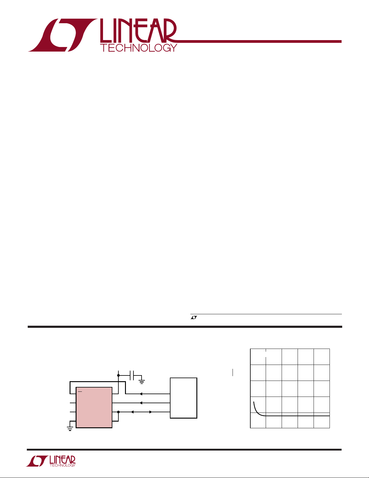
TYPICAL APPLICATION
5V
8
V
CC
(V
)
REF
7
CLK
6
D
OUT
5
D
IN
ANALOG INPUT #1
0V TO 5V RANGE
ANALOG INPUT #2
0V TO 5V RANGE
1
CS
2
CH0
LTC1091
3
CH1
4
GND
U
4.7µF
SERIAL DATA LINK
MPU
(e.g., 8051)
P1.4
P1.3
P1.2
FOR 8051 CODE SEE
APPLICATIONS INFORMATION
SECTION
1091 TA01
1.25
1024
1.00
0.75
0.50
0.25
0
VCC = 5V
0
1
2
REFERENCE VOLTAGE (V)
)
REF
1
LINEARITY ERROR (LSB = • V
3
4
5
1091 TA02
1
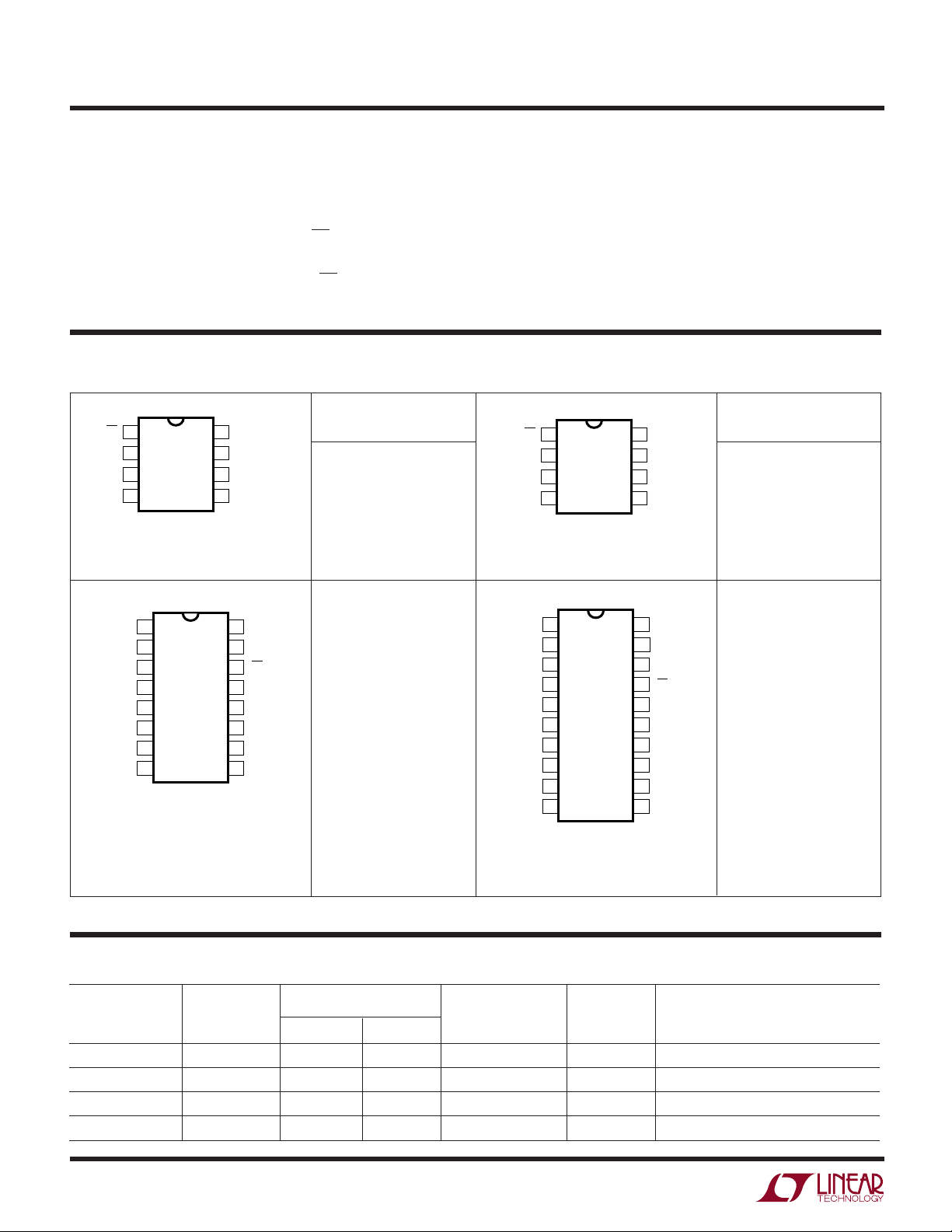
LTC1091/LTC1092
1
2
3
4
5
6
7
8
9
10
TOP VIEW
N PACKAGE
20-LEAD PDIP
20
19
18
17
16
15
14
13
12
11
CH0
CH1
CH2
CH3
CH4
CH5
CH6
CH7
COM
DGND
DV
CC
AV
CC
CLK
CS
D
OUT
D
IN
REF
+
REF
–
AGND
V
–
LTC1093/LTC1094
A
W
O
LUTEXI TIS
S
A
WUW
U
ARB
G
(Notes 1, 2)
Supply Voltage (VCC) to GND or V–........................ 12V
Negative Supply Voltage (V–).................... –6V to GND
Voltage
Analog Reference and LTC1091/2 CS
Inputs ................................. (V–) –0.3V to (V
+ 0.3V)
CC
Digital Inputs (except LTC1091/2 CS) .. –0.3V to 12V
Digital Outputs ........................ –0.3V to (V
+ 0.3V)
CC
WU
/
PACKAGE
1
CS
2
CH0
3
CH1
4
GND
T
= 110°C, θJA = 150°C/W (N)
JMAX
O
TOP VIEW
N8 PACKAGE
8-LEAD PDIP
RDER I FOR ATIO
ORDER PART
(V
)
V
8
CC
REF
CLK
7
D
6
OUT
D
5
IN
NUMBER
LTC1091ACN8
LTC1091CN8
Power Dissipation............................................. 500mW
Operating Temperature Range
LTC1091/2/3/4AC, LTC1091/2/3/4C..... –40°C to 85°C
Storage Temperature Range................ –65°C to 150°C
Lead Temperature (Soldering, 10 sec.)................ 300°C
U
TOP VIEW
1
CS
2
+IN
3
–IN
4
GND
N8 PACKAGE
8-LEAD PDIP
T
= 110°C, θJA = 150°C/W (N)
JMAX
V
8
CC
CLK
7
D
6
OUT
V
5
REF
ORDER PART
NUMBER
LTC1092ACN8
LTC1092CN8
TOP VIEW
1
CH0
2
CH1
3
CH2
4
CH3
5
CH4
6
CH5
7
COM
8
DGND
N PACKAGE
16-LEAD PDIP
T
T
JMAX
16-LEAD PLASTIC SO WIDE
= 110°C, θJA = 150°C/W (N)
JMAX
= 110°C, θJA = 130°C/W (SW)
16
15
14
13
12
11
10
9
SW PACKAGE
V
CC
CLK
CS
D
OUT
D
IN
V
REF
AGND
–
V
LTC1093ACN
LTC1093CN
LTC1093CSW
T
= 110°C, θJA = 150°C/W (N)
JMAX
LTC1094ACN
LTC1094CN
Consult factory for Industrial and Military grade parts.
PRODUCT GUIDE
PART NUMBER #CHANNELS UNIPOLAR BIPOLAR (SEPARATE V
LTC1091 2 ● Pin-for-Pin 10-Bit Upgrade of ADC0832
LTC1092 1 ●●Pin-for-Pin 10-Bit Upgrade of ADC0831
LTC1093 6 ●● ● ●
LTC1094 8 ●● ● ●
2
CONVERSION MODES
REDUCED SPAN
CAPABILITY
REF
±
5V
) CAPABILITY
LTC1091/LTC1092
LTC1093/LTC1094
UUUUWW
RECO E DED OPERATI G CO DITIO S
LTC1091A/LTC1092A/LTC1093A/LTC1094A
SYMBOL PARAMETER CONDITIONS MIN MAX UNITS
V
CC
–
V
f
CLK
t
CYC
t
hDI
t
suCS
t
suDI
t
WHCLK
t
WLCLK
t
WHCS
t
WLCS
Supply Voltage 4.5 10 V
Negative Supply Voltage LTC1093/LTC1094, VCC = 5V –5.5 0 V
Clock Frequency VCC = 5V 0.01 0.5 MHz
Total Cycle Time LTC1091 15 CLK Cycles
Hold Time, DIN Alter SCLK↑ VCC = 5V 150 ns
Setup Time CS↓ Before CLK↑ VCC = 5V 1 µs
Setup Time DIN Stable Before CLK↑ VCC = 5V 400 ns
CLK High Time VCC = 5V 0.8 µs
CLK Low Time VCC = 5V 1 µs
CS High Time Between Data Transfer Cycles VCC = 5V 2 µs
CS Low Time During Data Transfer LTC1091 15 CLK Cycles
LTC1091/LTC1092/LTC1093/LTC1094
+ 2µs
LTC1092 12 CLK Cycles
+ 2µs
LTC1093/LTC1094 18 CLK Cycles
+ 2µs
LTC1092 12 CLK Cycles
LTC1093/LTC1094 18 CLK Cycles
UW
U
CONVERTER AND MULTIPLEXER CHARACTERISTICS
The ● denotes specifications which apply over the full operating temperature range, otherwise specifications are TA = 25°C. (Note 3)
LTC1091A/LTC1092A LTC1091/LTC1092
LTC1093A/LTC1094A LTC1093/LTC1094
PARAMETER CONDITIONS MIN TYP MAX MIN TYP MAX UNITS
Offset Error (Note 4) ● ±0.5 ±0.5 LSB
Linearity Error (Notes 4, 5) ● ±0.5 ±0.5 LSB
Full-Scale Error (Note 4) ● ±1.0 ±2.0 LSB
Total Unadjusted Error V
Reference Input Resistance LTC1092/LTC1093/LTC1094 ● 510 510 kΩ
Analog and REF Input Range (Note 7) (V–) –0.05V to VCC + 0.05V V
On-Channel Leakage Current On-Channel = 5V ● 11µA
(Note 8) Off-Channel = 0V
Off-Channel Leakage Current On-Channel = 5V ● –1 –1 µA
(Note 8) Off-Channel = 0V
= 5.000V (Notes 4, 6) ● ±1.0 LSB
REF
V
= 5V
REF
On-Channel = 0V ● –1 –1 µA
Off-Channel = 5V
On-Channel = 0V ● 11µA
Off-Channel = 5V
3
LTC1091/LTC1092
LTC1093/LTC1094
AC CHARACTERISTICS
The ● denotes specifications which apply over the full operating temperature range, otherwise specifications are TA = 25°C. (Note 3)
LTC1091A/LTC1092A/LTC1093A/LTC1094A
SYMBOL PARAMETER CONDITIONS MIN TYP MAX UNITS
t
SMPL
t
CONV
t
dDO
t
dis
t
en
t
hDO
t
f
t
r
C
IN
Analog Input Sample Time See Operating Sequence 1.5 CLK Cycles
Conversion Time See Operating Sequence 10 CLK Cycles
Delay Time, CLK↓ to D
Delay Time, CS↑ to D
Delay Time, CLK↓ to D
Time Output Data Remains Valid After SCLK↓ 150 ns
D
Fall Time See Test Circuits ● 90 300 ns
OUT
D
Rise Time See Test Circuits ● 60 300 ns
OUT
Input Capacitance Analog Inputs On-Channel 65 pF
Data Valid See Test Circuits ● 400 850 ns
OUT
Hi-Z See Test Circuits ● 180 450 ns
OUT
Enabled See Test Circuits ● 160 450 ns
OUT
LTC1091/LTC1092/LTC1093/LTC1094
Analog Inputs Off-Channel 5 pF
Digital Inputs 5 pF
U
DIGITAL
A
DC
D
The ● denotes specifications which apply over the full operating temperature range, otherwise specifications are TA = 25°C. (Note 3)
SYMBOL PARAMETER CONDITIONS MIN TYP MAX UNITS
V
IH
V
IL
I
IH
I
IL
V
OH
V
OL
I
OZ
I
SOURCE
I
SINK
I
CC
I
REF
–
I
Note 1: Absolute Maximum Ratings are those values beyond which the life
of a device may be impaired.
Note 2: All voltage values are with respect to ground with DGND, AGND,
GND and REF
connected to the AGND pin on the LTC1093. DGND, AGND, REF
are internally connected to the GND pin on the LTC1091/LTC1092.
Note 3: V
–5V for bipolar mode, CLK = 0.5MHz unless otherwise specified.
Note 4: These specs apply for both unipolar (LTC1091/LTC1092/LTC1093/
LTC1094) and bipolar (LTC1093/LTC1094 only) modes. In bipolar mode,
one LSB is equal to the bipolar input span (2V
example, when V
Note 5: Linearity error is specified between the actual end points of the
A/D transfer curve.
High Level Input Voltage VCC = 5.25V ● 2.0 V
Low Level Input Voltage VCC = 4.75V ● 0.8 V
High Level Input Current VIN = V
Low Level Input Current VIN = 0V ● –2.5 µA
High Level Output Voltage VCC = 4.75V, I
Low Level Output Voltage VCC = 4.75V, I
Hi-Z Output Leakage V
Output Source Current V
Output Sink Current V
Positive Supply Current LTC1091, CS High ● 1.5 3.5 mA
Reference Current LTC1092/LTC1093/LTC1094, V
Negative Supply Current LTC1093/LTC1094, CS High, V– = –5V ● 150µA
–
wired together (unless otherwise noted). REF– is internally
= 5V, V
CC
+
= 5V, V
REF
= 5V, 1LSB (bipolar) = 2(5V)/1024 = 9.77mV.
REF
REF
LECTRICAL C CHARA TER ST
E
CC
= 10µA 4.7 V
= 4.75V, I
V
CC
= VCC, CS High ● 3 µA
OUT
V
= 0V, CS High ● –3 µA
OUT
= 0V –10 mA
OUT
= V
OUT
LTC1092/LTC1093/LTC1094, CS High, REF+ Open ● 1.0 2.5 mA
–
= 0V, V– = 0V for unipolar mode and
REF
OUT
= 360µA ● 2.4 4.0 V
OUT
= 1.6mA ● 0.4 V
OUT
CC
–
and V
) divided by 1024. For
= 5V ● 0.5 1.0 mA
REF
Note 6: Total unadjusted error includes offset, full scale, linearity,
multiplexer and hold step errors.
Note 7: Two on-chip diodes are tied to each reference and analog input
which will conduct for reference or analog input voltages one diode drop
–
–
below V
VCC levels (4.5V), as high level reference or analog inputs (5V) can cause
this input diode to conduct, especially at elevated temperatures, and cause
errors for inputs near full scale. This spec allows 50mV forward bias of
either diode. This means that as long as the reference or analog input does
not exceed the supply voltage by more than 50mV, the output code will be
correct. To achieve an absolute 0V to 5V input voltage range will therefore
require a minimum supply voltage of 4.950V over initial tolerance,
temperature variations and loading.
Note 8: Channel leakage current is measured after the channel selection.
or one diode drop above VCC. Be careful during testing at low
ICS
I
LTC1091A/LTC1092A/LTC1093A/LTC1094A
LTC1091/LTC1092/LTC1093/LTC1094
● 2.5 µA
10 mA
4
LPER
LTC1091/LTC1092
LTC1093/LTC1094
UW
R
F
O
ATYPICA
CCHARA TERIST
E
C
ICS
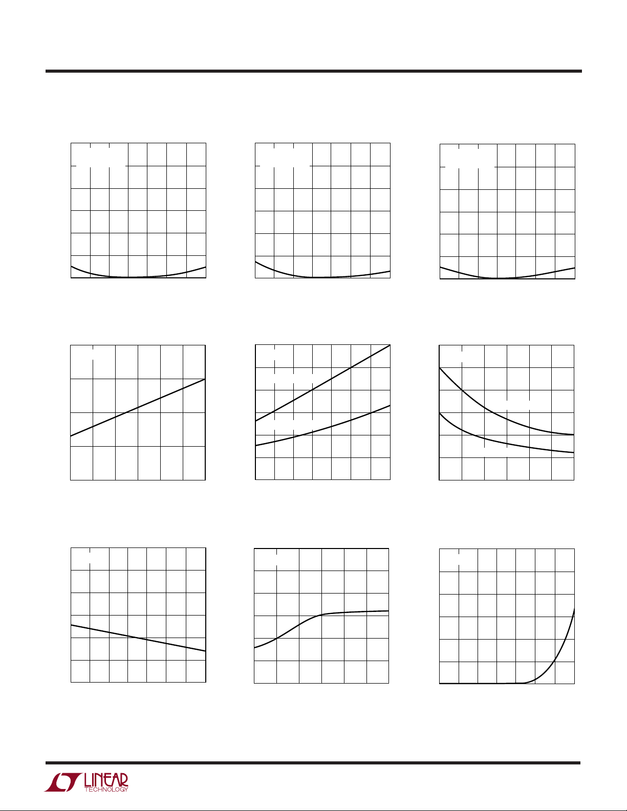
Change in Offset Error vs
Temperature
0.6
VCC (V
) = 5V
REF
= 500kHz
f
CLK
0.5
0.4
0.3
0.2
0.1
MAGNITUDE OF OFFSET CHANGE (LSB)
0
–50
–25
25
0
AMBIENT TEMPERATURE (°C)
50
Digital Input Logic Threshold vs
Supply Voltage
4
TA = 25°C
3
2
LOGIC THRESHOLD (V)
1
0
4
678
5
SUPPLY VOLTAGE (V)
Maximum Clock Rate vs
Temperature
3.0
VCC = 5V
2.5
75
1091/2/3/4 G01
1091/2/3/4 G04
125100
910
Change in Linearity Error vs
Temperature
0.6
VCC (V
) = 5V
REF
= 500kHz
f
CLK
0.5
0.4
0.3
0.2
0.1
MAGNITUDE OF LINEARITY CHANGE (LSB)
DELAY TIME FROM SCLK↓ (ns)
OUT
D
600
500
400
300
200
100
0
0
–50
–50
–25
D
Delay Time vs Temperature
OUT
VCC = 5V
MSB-FIRST DATA
LSB-FIRST DATA
–25
25
50
0
AMBIENT TEMPERATURE (°C)
25
0
AMBIENT TEMPERATURE (°C)
75
50
75
Maximum Clock Rate vs
Supply Voltage
3.0
TA = 25°C
2.5
1091/2/3/4 G02
1091/2/3/4 G05
Change in Full-Scale Error vs
Temperature
0.6
VCC (V
) = 5V
REF
= 500kHz
f
CLK
0.5
0.4
0.3
0.2
0.1
MAGNITUDE OF FULL-SCALE CHANGE (LSB)
125100
0
–50
–25
D
Delay Time vs
OUT
25
50
0
AMBIENT TEMPERATURE (°C)
75
125100
1091/2/3/4 G03
Supply Voltage
600
TA = 25°C
500
400
300
200
DELAY TIME FROM SCLK↓ (ns)
100
OUT
D
125100
0
4
MSB-FIRST DATA
LSB-FIRST DATA
678
5
SUPPLY VOLTAGE (V)
910
1091/2/3/4 G06
Minimum Clock Rate vs
Temperature
0.3
VCC = 5V
0.25
2.0
1.5
1.0
0.5
MAXIMUM CLK FREQUENCY* (MHz)
0
–50
–25
*MAXIMUM CLK FREQUENCY REPRESENTS THE HIGHEST FREQUENCY AT WHICH CLK CAN
BE OPERATED (WITH 50% DUTY CYCLE) WHILE STILL PROVIDING 100ns SETUP TIME FOR
THE DEVICE RECEIVING THE D
25
50
OUT
75
DATA.
0
AMBIENT TEMPERATURE (°C)
125100
1091/2/3/4 G07
2.0
1.5
1.0
0.5
MAXIMUM CLK FREQUENCY* (MHz)
0
4
678
5
SUPPLY VOLTAGE (V)
0.20
0.15
0.10
0.05
MINIMUM CLK FREQUENCY** (MHz)
910
1091/2/3/4 G08
**AS THE CLK FREQUENCY IS DECREASED FROM 500kHz, MINIMUM CLK FREQUENCY
(∆ERROR ≤ 0.1LSB) REPRESENTS THE FREQUENCY AT WHICH A 0.1LSB SHIFT IN ANY
CODE TRANSITION FROM ITS 500kHz VALUE IS FIRST DETECTED.
0
–50
0
–25
AMBIENT TEMPERATURE (°C)
25
50
75
1091/2/3/4 G09
5
125100
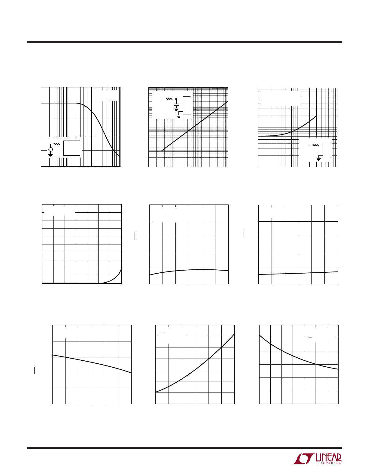
LTC1091/LTC1092
R
SOURCE
+
(Ω)
100 1k 10k
1091/2/3/4 G12
0.1
S & H ACQUISITION TIME TO 0.1% (µs)
1
10
+
–
V
IN
R
SOURCE
+
VCC = 5V
T
A
= 25°C
0V TO 5V INPUT STEP
SUPPLY VOLTAGE (V)
4
LINEARITY ERROR [LSB = • V
CC
(V
REF
)]
1.25
1.00
0.75
0.5
0.25
0
5
678
1091/2/3/4 G15
910
f
CLK
= 500kHz
T
A
= 25°C
1
1024
LTC1093/LTC1094
LPER
R
F
O
ATYPICA
UW
CCHARA TERIST
E
C
ICS
LTC1091/LTC1092/LTC1093/LTC1094
Maximum Clock Rate vs
Source Resistance
1.25
1.00
(MHz)
†
0.75
0.50
R
SOURCE
“+” OR “–”
INPUT
V
0.25
MAXIMUM CLK FREQUENCY
0
IN
10
100 1k 10k
R
SOURCE
VCC = 5V
T
(Ω)
LTC1091/LTC1092 Input Channel
Leakage Current vs Temperature
100
ON-CHANNEL OR
OFF-CHANNEL
80
60
= 25°C
A
1091/2/3/4 G10
LTC1091/LTC1092/LTC1093/LTC1094
Maximum Filter Resistor vs
Cycle Time
100k
10k
(Ω)
††
FILTER
1k
100
MAXIMUM R
10
R
FILTER
V
C
FILTER
IN
≥1µF
+
–
10 1000 10000
100
CYCLE TIME (µs)
LTC1091 Offset Error vs
Supply Voltage
1.25
)]
f
= 500kHz
CLK
= 25°C
T
REF
A
(V
1
CC
1024
1.00
0.75
OS
= 0.85mV AT VCC (V
V
REF
) = 5V
LTC1091/LTC1092/LTC1093/LTC1094
Sample-and-Hold Acquisition Time
vs Source Resistance
1091/2/3/4 G11
LTC1091 Linearity Error vs
Supply Voltage
40
20
INPUT CHANNEL LEAKAGE CURRENT (nA)
0
–50
–25
25
0
AMBIENT TEMPERATURE (°C)
LTC1091 Change in Full-Scale
Error vs Supply Voltage
0.50
f
= 500kHz
CLK
= 25°C
T
A
0.25
)]
REF
(V
0
CC
1
–0.25
1024
[LSB = • V
–0.50
CHANGE IN FULL-SCALE ERROR
–0.75
4
†
AS THE CLK FREQUENCY AND SOURCE RESISTANCE ARE INCREASED, MAXIMUM CLK
FREQUENCY (∆ERROR ≤ 0.1LSB) REPRESENTS THE FREQUENCY AT WHICH A 0.1LSB
SHIFT IN ANY CODE TRANSITION FROM ITS 500kHz, 0Ω VALUE IS FIRST DETECTED.
6
678
5
SUPPLY VOLTAGE (V)
50
0.5
0.25
OFFSET ERROR [LSB = • V
75
125100
1091/2/3/4 G13
910
1091/2/3/4 G16
0
4
678
5
SUPPLY VOLTAGE (V)
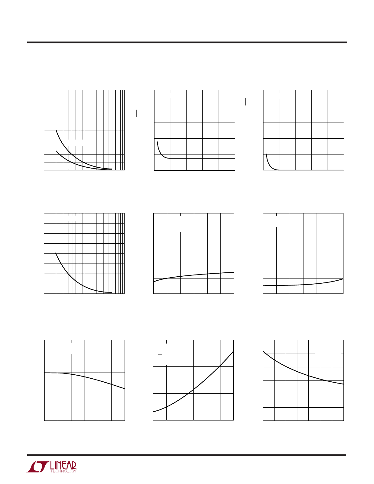
LTC1091 Supply Current vs
Supply Voltage
7
f
= 500kHz
CLK
CS = V
(V
6
T
= 25°C
A
5
4
3
2
SUPPLY CURRENT (mA)
1
0
4
5
)
CC
REF
678910
SUPPLY VOLTAGE (V)
††
MAXIMUM R
CHANGE IN FULL-SCALE ERROR FROM ITS VALUE AT R
910
1091/2/3/4 G14
LTC1091 Supply Current vs
Temperature
1.8
1.6
1.4
1.2
1.0
SUPPLY CURRENT (mA)
0.8
0.6
–50
1092/2/3/4 G17
REPRESENTS THE FILTER RESISTOR VALUE AT WHICH A 0.1LSB
FILTER
0
–25
AMBIENT TEMPERATURE (°C)
FILTER
f
CLK
V
CS = 5V
25
50
= 0 IS FIRST DETECTED.
= 500kHz
(V
CC
75
) = 5V
REF
1091/2/3/4 G18
125100
LPER
LTC1091/LTC1092
LTC1093/LTC1094
UW
R
F
O
ATYPICA
CCHARA TERIST
E
C
ICS
LTC1092/LTC1093/LTC1094
Unadjusted Offset Error vs
Reference Voltage
10
VCC = 5V
9
)
REF
8
7
1
1024
6
5
4
3
2
OFFSET ERROR (LSB = • V
1
0
0.1 0.2 1 5 10
VOS = 1mV
VOS = 0.5mV
REFERENCE VOLTAGE (V)
LTC1092/LTC1093/LTC1094
Noise Error vs Reference Voltage
2.00
NOISE = 200µV
1.75
1.50
1.25
1.00
0.75
0.50
PEAK-TO-PEAK NOISE ERROR (LSB)
0.25
0
0.1 0.2 1 5 10
P-P
REFERENCE VOLTAGE (V)
LTC1092/LTC1093/LTC1094
Change in Full-Scale Error vs
Supply Voltage
0.50
V
= 4V
REF
= 500kHz
f
CLK
0.25
0
–0.25
–0.50
CHANGE IN FULL-SCALE ERROR (LSB)
–0.75
4
678
5
SUPPLY VOLTAGE (V)
1091/2/3/4 G19
1091/2/3/4 G22
910
1091/2/3/4 G25
LTC1092/LTC1093/LTC1094
Linearity Error vs
Reference Voltage
1.25
1.00
1024
0.75
0.50
0.25
0
VCC = 5V
0
1
2
REFERENCE VOLTAGE (V)
)
REF
1
LINEARITY ERROR (LSB = • V
LTC1092/LTC1093/LTC1094
Offset Error vs Supply Voltage
1.25
V
= 4V
REF
= 500kHz
f
CLK
= 1.25mV AT VCC = 5V
V
OS
1.00
0.75
0.50
OFFSET ERROR (LSB)
0.25
0
4
678
5
SUPPLY VOLTAGE (V)
LTC1092/LTC1093/LTC1094
Supply Current vs Supply Voltage
6
V
OPEN
REF
= 500kHz
f
CLK
5
CS = V
CC
TA = 25°C
4
3
2
SUPPLY CURRENT (mA)
1
0
4
678
5
SUPPLY VOLTAGE (V)
3
4
5
1092/2/3/4 G20
910
1091/2/3/4 G23
910
1091/2/3/4 G26
LTC1092/LTC1093/LTC1094
Change in Full-Scale Error vs
Reference Voltage
)
1.25
REF
1
CHANGE IN FULL-SCALE ERROR (LSB = • V
1024
1.00
0.75
0.50
0.25
0
0
VCC = 5V
1
REFERENCE VOLTAGE (V)
3
2
LTC1092/LTC1093/LTC1094
Linearity Error vs Supply Voltage
1.25
V
= 4V
REF
= 500kHz
f
CLK
1.00
0.75
0.50
LINEARITY ERROR (LSB)
0.25
0
4
678
5
SUPPLY VOLTAGE (V)
LTC1092/LTC1093/LTC1094
Supply Current vs Temperature
1.4
1.2
1.0
0.8
0.6
SUPPLY CURRENT (mA)
0.4
0.2
–50
0
–25
AMBIENT TEMPERATURE (°C)
25
V
REF
f
CLK
CS = 5V
V
CC
50
75
4
1092/2/3/4 G21
910
1091/2/3/4 G24
OPEN
= 500kHz
= 5V
1091/2/3/4 G27
5
125100
7
LTC1091/LTC1092
LTC1093/LTC1094
LPER
R
F
O
ATYPICA
UW
CCHARA TERIST
E
C
ICS
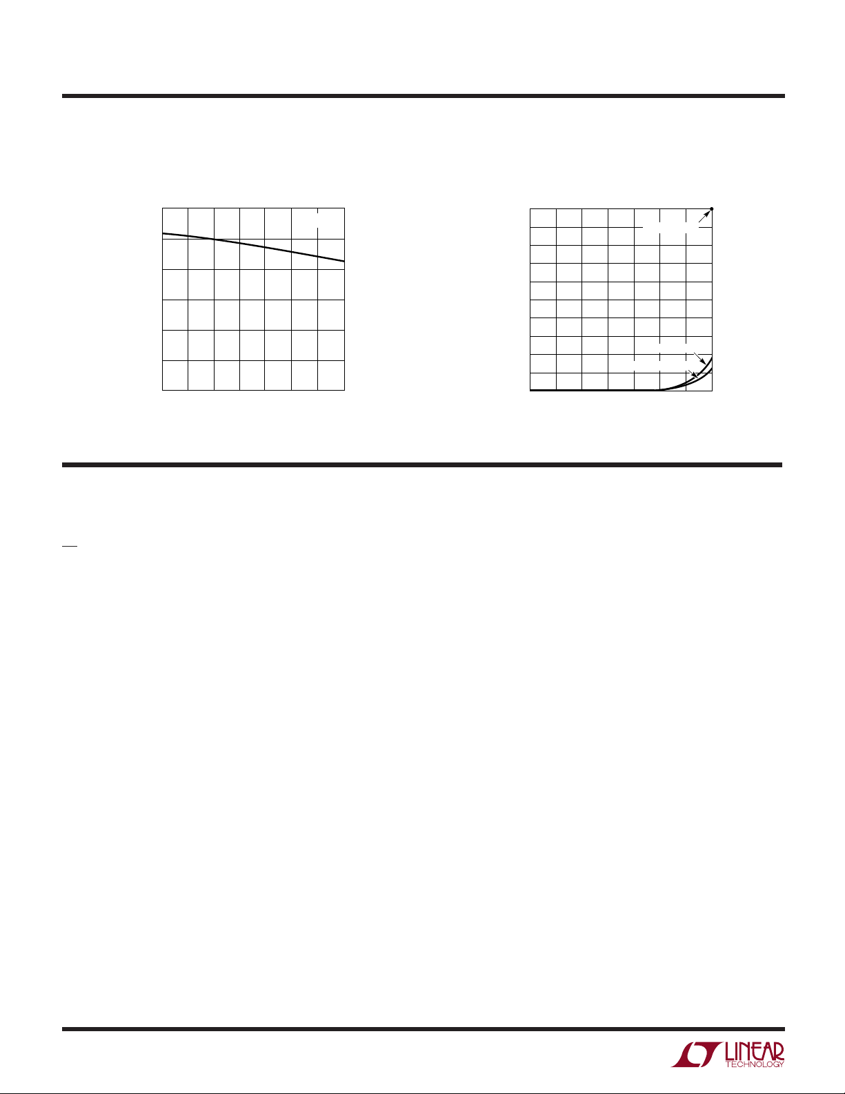
LTC1092/LTC1093/LTC1094
Reference Current vs Temperature
0.6
0.5
0.4
0.3
0.2
REFERENCE CURRENT (mA)
0.1
0
–50
U
25
0
–25
AMBIENT TEMPERATURE (°C)
UU
V
= 5V
REF
50
75
125100
1091/2/3/4 G28
PI FU CTIO S
LTC1091/LTC1092
CS (Pin 1): Chip Select Input. A logic low on this input
enables the LTC1091/LTC1092.
CH0, CH1/+ IN, – IN (Pins 2, 3): Analog Inputs. These
inputs must be free of noise with respect to GND.
LTC1093/LTC1094 Input Channel
Leakage Current vs Temperature
1000
900
800
700
600
500
400
300
200
100
INPUT CHANNEL LEAKAGE CURRENT (nA)
0
–50
0
–25
AMBIENT TEMPERATURE (°C)
GUARANTEED
ON-CHANNEL
OFF-CHANNEL
75
50 125
25
100
1091/2/3/4 G29
VCC (Pin 8 )(LTC1092): Positive Supply Voltage. This pin
provides power to the A/D converter. It must be kept free
of noise and ripple by bypassing directly to the analog
ground plane.
GND (Pin 4): Analog Ground. GND should be tied directly
to an analog ground plane.
DIN (Pin 5)(LTC1091): Digital Data Input. The multiplexer
address is shifted into this input.
V
(Pin 5)(LTC1092): Reference Input. The reference
REF
input defines
the span of the A/D converter and must be
kept free of noise with respect to AGND.
D
(Pin 6): Digital Data Output. The A/D conversion
OUT
result is shifted out of this output.
CLK (Pin 7): Shift Clock. This clock synchronizes the serial
data transfer.
VCC(V
)(Pin 8)(LTC1091): Positive Supply and Refer-
REF
ence Voltage. This pin provides power and defines the
span of the A/D converter. It must be kept free of noise and
ripple by bypassing directly to the analog ground plane.
LTC1093/LTC1094
CH0 to CH5/CH0 to CH7 (Pins 1 to 6/Pins 1 to 8): Analog
Inputs. The analog inputs must be free of noise with
respect to AGND.
COM (Pin 7/Pin 9): Common. The common pin defines the
zero reference point for all single-ended inputs. It must be
free of noise and is usually tied to the analog ground plane.
DGND (Pin 8/Pin 10): Digital Ground. This is the ground
for the internal logic. Tie to the ground plane.
V– (Pin 9/Pin 11): Negative Supply. Tie V– to most
negative potential in the circuit. (Ground in single supply
applications.)
AGND (Pin 10/Pin 12): Analog Ground. AGND should be
tied directly to the analog ground plane.
8
LTC1091/LTC1092
LTC1093/LTC1094
U
UU
PI FU CTIO S
V
(Pin 11)(LTC1093): Reference Input. The reference
REF
input must be kept free of noise with respect to AGND.
REF+, REF– (Pins 13, 14 )(LTC1094): Reference Input.
The reference input must be kept free of noise with respect
to AGND.
DIN (Pin 12/Pin 15): Data Input. The A/D configuration
word is shifted into this input.
D
(Pin 13/Pin 16): Digital Data Output. The A/D con-
OUT
version result is shifted out of this output.
CS (Pin 14/Pin 17): Chip Select Input. A logic low on this
input enables the LTC1093/LTC1094.
W
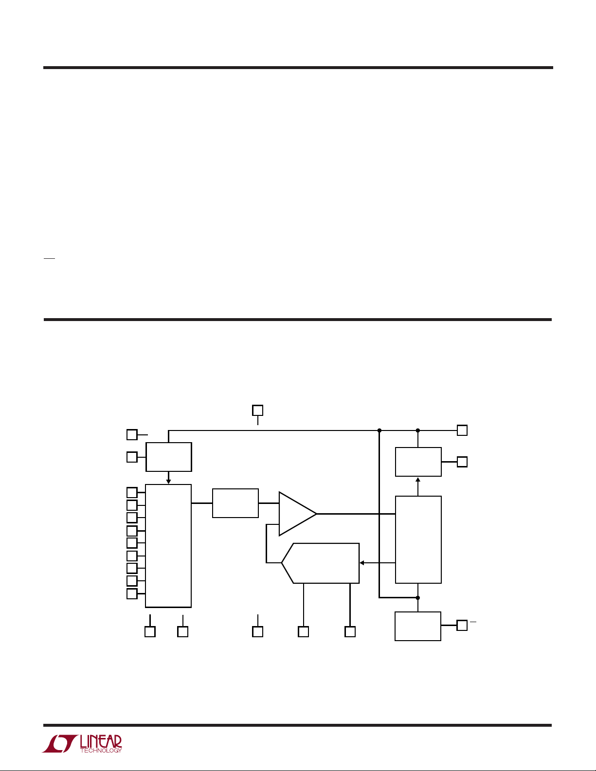
BLOCK DIAGRA
(Pin numbers refer to LTC1094)
CLK (Pin 15/Pin 18): Shift Clock. This clock synchronizes
the serial data transfer.
VCC (Pin 16)(LTC1093): Positive Supply. This supply
must be kept free of noise and ripple by bypassing directly
to the analog ground plane.
AVCC, DVCC (Pins 19, 20)(LTC1094): Positive Supply.
This supply must be kept free of noise and ripple by
bypassing directly to the analog ground plane. AVCC and
DVCC should be tied together on the LTC1094.
AV
CH0
CH1
CH2
CH3
CH4
CH5
CH6
CH7
COM
DV
CC
19
18
16
17
1091/2/3/4 BD
CLK
D
CS
OUT
20
CC
INPUT
REGISTER
ANALOG
INPUT MUX
10
DGND
SHIFT
SAMPLE-
AND-HOLD
11 12 13 14
–
V
AGND
COMP
CAPACITIVE
–
REF
10-BIT
DAC
REF
+
15
D
IN
1
2
3
4
5
6
7
8
9
OUTPUT
SHIFT
REGISTER
10-BIT
SAR
CONTROL
AND
TIMING
9
LTC1091/LTC1092
D
OUT
WAVEFORM 1
(SEE NOTE 1)
2.0V
t
dis
90%
10%
D
OUT
WAVEFORM 2
(SEE NOTE 2)
CS
NOTE 1: WAVEFORM 1 IS FOR AN OUTPUT WITH INTERNAL CONDITIONS SUCH THAT
THE OUTPUT IS HIGH UNLESS DISABLED BY THE OUTPUT CONTROL
NOTE 2: WAVEFORM 2 IS FOR AN OUTPUT WITH INTERNAL CONDITIONS SUCH THAT
THE OUTPUT IS LOW UNLESS DISABLED BY THE OUTPUT CONTROL
1091/2/3/4 TC06
LTC1093/LTC1094
TEST CIRCUITS
On- and Off-Channel Leakage Current
5V
POLARITY
Voltage Waveforms for D
D
CLK
OUT
0.8V
t
dDO
Load Circuit for t
I
ON
A
I
OFF
A
ON-CHANNEL
OFFCHANNELS
1091/2/3/4 TC01
D
OUT
Voltage Waveforms for D
Delay Time, t
OUT
dDO
2.4V
D
OUT
t
r
1.4V
OUT
Voltage Waveforms for t
0.4V
1091/2/3/4 TC03
, tr, t
dDO
3k
100pF
f
TEST POINT
1091/2/3/4 TC02
Rise and Fall Times, tr, t
2.4V
0.4V
t
f
1091/2/3/4 TC04
dis
f
Load Circuit for t
TEST POINT
D
D
CLK
OUT
3k
100pF
CS
IN
LTC1091
D
OUT
dis
, t
5V t
START
en
WAVEFORM 2, t
dis
t
WAVEFORM 1
dis
1
en
1091/2/3/4 TC05
Voltage Waveforms for t
2
34
en
B9
0.4V
t
en
1091/2/3/4 TC07
10
 Loading...