

Linear Technology LTC1090MJ, LTC1090CSW, LTC1090CN, LTC1090AMJ, LTC1090ACN Datasheet
...
FEATURES
■
Software Programmable Features:
Unipolar/Bipolar Conversions
4 Differential/8 Single Ended Inputs
MSB or LSB First Data Sequence
Variable Data Word Length
■
Built-In Sample and Hold
■
Single Supply 5V, 10V or ±5V Operation
■
Direct 4 Wire Interface to Most MPU Serial Ports and
All MPU Parallel Ports
■
30kHz Maximum Throughput Rate
U
KEY SPECIFICATIO S
■
Resolution: 10 Bits
■
Total Unadjusted Error (LTC1090A): ±1/2LSB Max
■
Conversion Time: 22µs
■
Supply Current: 2.5mA Max, 1.0mA Typ
, LTC and LT are registered trademarks of Linear Technology Corporation.
LTCMOS is a trademark of Linear Technology Corp.
LTC1090
Single Chip 10-Bit Data
Acquisition System
U
DESCRIPTIO
The LTC®1090 is a data acquisition component which
contains a serial I/O successive approximation A/D converter. It uses LTCMOSTM switched capacitor technology
to perform either 10-bit unipolar, or 9-bit plus sign bipolar
A/D conversions. The 8-channel input multiplexer can be
configured for either single ended or differential inputs (or
combinations thereof). An on-chip sample and hold is
included for all single ended input channels.
The serial I/O is designed to be compatible with industry
standard full duplex serial interfaces. It allows either
MSB or LSB first data and automatically provides 2’s
complement output coding in the bipolar mode. The
output data word can be programmed for a length of 8, 10,
12 or 16 bits. This allows easy interface to shift registers
and a variety of processors.
The LTC1090A is specified with total unadjusted error
(including the effects of offset, linearity and gain errors)
less than ±0.5LSB.
The LTC1090 is specified with offset and linearity less than
±0.5LSB but with a gain error limit of ±2LSB for
applications where gain is adjustable or less critical.
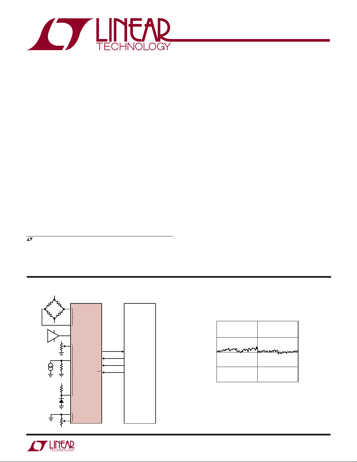
TYPICAL APPLICATIO
LTC1090 MPU
DIFFERENTIAL
INPUT
5V
BIPOLAR INPUT
5V
–5V
OUT
T
–5V
(+)
(–)
UNIPOLAR
INPUTS
– UNIPOLAR
INPUT
IN
SERIAL DATA
U
FOR 8051 CODE SEE
APPLICATIONS INFORMATION
SECTION
(e.g., 8051)
P1.1D
P1.2D
P1.3SCLK
P1.4CS
LINK
LTC1090 • TA01
Linearity Plot
1.0
0.5
0.0
ERROR (LSBs)
–0.5
–1.0
0 512 1024
OUTPUT CODE
LTC1090 • TA02
1090fc
1
LTC1090
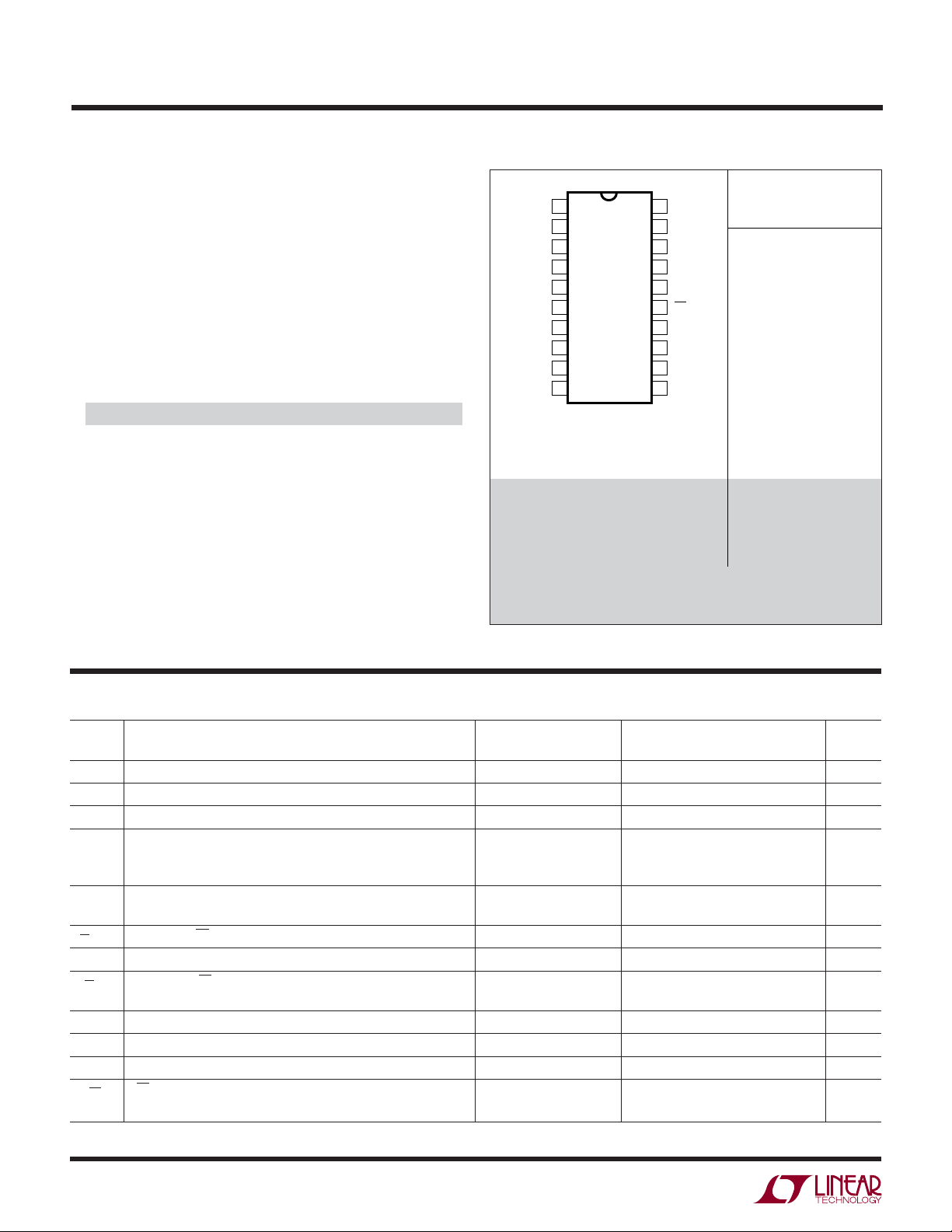
PACKAGE/ORDER I FOR ATIO
UU
W
WWWU
ABSOLUTE AXI U RATI GS
(Notes 1 and 2)
Supply Voltage (VCC) to GND or V
Negative Supply Voltage (V
Voltage:
Analog and Reference
Inputs .................................... (V–) –0.3V to V
Digital Inputs .........................................–0.3V to 12V
Digital Outputs ..............................– 0.3V to V
Power Dissipation.............................................. 500mW
Operating Temperature Range
LTC1090AC/LTC1090C ........................–40°C to 85°C
LTC1090AM/LTC1090M (OBSOLETE) ...... –55°C to 125°C
Storage Temperature Range ................. –65°C to 150°C
Lead Temperature (Soldering, 10 sec).................. 300°C
–
–
) ..................... – 6V to GND
................................
CC
CC
12V
0.3V
0.3V
TOP VIEW
1
CH0
2
CH1
3
CH2
4
CH3
5
CH4
6
CH5
7
CH6
8
CH7
9
COM
10
DGND
SW PACKAGE
20-LEAD PLASTIC SO WIDE
T
= 150°C, θ
JMAX
T
= 110°C, θ
JMAX
20-LEAD PDIP
= 70°C/W
JA
= 90°C/W
JA
V
20
CC
ACLK
19
SCLK
18
D
17
IN
D
16
OUT
CS
15
REF
14
REF
13
–
V
12
AGND
11
N PACKAGE
ORDER PART
NUMBER
LTC1090ACN
LTC1090CN
LTC1090CSW
+
–
20-LEAD CERDIP
T
= 150°C θ
JMAX
J PACKAGE
JA
= 70° C/W
LTC1090AMJ
LTC1090MJ
LTC1090ACJ
LTC1090CJ
OBSOLETE PACKAGE
Consider the SW or N Package for Alternate Source
Consult LTC Marketing for parts specified with wider operating temperature
ranges.
LTC1090 • POI01
UUUUWW
RECO E DED OPERATI G CO DITIO S
LTC1090/LTC1090A
SYMBOL PARAMETER CONDITIONS MIN MAX UNITS
V
CC
–
V
f
SCLK
f
ACLK
t
CYC
t
hCS
t
hDI
t
suCS
t
suDI
t
WHACLK
t
WLACLK
t
WHCS
Positive Supply Voltage V– = 0V 4.5 10 V
Negative Supply Voltage VCC = 5V –5.5 0 V
Shift Clock Frequency VCC = 5V 0 1.0 MHz
A/D Clock Frequency VCC = 5V 25°C 0.01 2.0 MHz
85°C 0.05 2.0
125°C 0.25 2.0
Total Cycle Time See Operating Sequence 10 SCLK + Cycles
48 ACLK
Hold Time, CS Low After Last SCLK
Hold Time, DIN After SCLK
Setup Time CS↓ Before Clocking in First Address Bit (Note 9) VCC = 5V 2 ACLK Cycles
Setup Time, DIN Stable Before SCLK
ACLK High Time VCC = 5V 127 ns
ACLK Low Time VCC = 5V 200 ns
CS High Time During Conversion VCC = 5V 44 ACLK
↑
↓
↑
VCC = 5V 0 ns
VCC = 5V 150 ns
1µs
VCC = 5V 400 ns
Cycles
2
1090fc
LTC1090
W
U
CO VERTER A D ULTIPLEXER CHARACTERISTICS
apply over the full operating temperature range, otherwise specifications are T
PARAMETER CONDITIONS MIN TYP MAX MIN TYP MAX UNITS
Offset Error (Note 4) ● ±0.5 ±0.5 LSB
Linearity Error (Notes 4 and 5) ● ±0.5 ±0.5 LSB
Gain Error (Note 4) ● ±1.0 ±2.0 LSB
Total Unadjusted Error V
Reference Input Resistance 10 10 kΩ
Analog and REF Input Range (Note 7) (V–) – 0.05V to VCC 0.05V V
On Channel Leakage Current On Channel = 5V ● 11µA
(Note 8) Off Channel = 0V
Off Channel Leakage Current On Channel = 5V ● –1 –1 µA
(Note 8) Off Channel = 0V
U
The ● denotes specifications which
= 25°C. (Note 3)
A
LTC1090A LTC1090
= 5.000V ● ±1.0 LSB
REF
(Notes 4 and 6)
On Channel = 0V ● –1 –1 µA
Off Channel = 5V
On Channel = 0V ● 11µA
Off Channel = 5V
AC ELECTRICAL CHARACTERISTICS
The ● denotes specifications which apply over the full operating
temperature range, otherwise specification are TA = 25°C. (Note 3)
SYMBOL PARAMETER CONDITIONS MIN TYP MAX UNITS
t
ACC
t
SMPL
t
CONV
t
dDO
t
dis
t
en
t
hDO
t
f
t
r
C
IN
Delay Time From CS↓ to D
Analog Input Sample Time See Operating Sequence 5 SCLK Cycles
Conversion Time See Operating Sequence 44 ACLK Cycles
Delay Time, SCLK↓ to D
Delay Time, CS↑ to D
Delay Time, 2nd CLK↓ to D
Time Output Data Remains Valid After SCLK
D
Fall Time See Test Circuits ● 90 300 ns ns
OUT
D
Rise Time See Test Circuits ● 60 300 ns ns
OUT
Input Capacitance Analog Inputs On Channel 65 pF
Data Valid (Note 9) 2 ACLK Cycles
OUT
Data Valid See Test Circuits ● 250 450 ns
OUT
Hi-Z See Test Circuits ● 140 300 ns ns
OUT
Enabled See Test Circuits ● 150 400 ns ns
OUT
↓
Digital Inputs 5 pF
Off Channel 5 pF
LTC1090/LTC1090A
50 ns
1090fc
3
LTC1090
U
DIGITAL A D DC ELECTRICAL CHARACTERISTICS
over the full operating temperature range, otherwise specification are T
= 25°C. (Note 3)
A
The ● denotes specifications which apply
SYMBOL PARAMETER CONDITIONS MIN TYP MAX UNITS
LTC1090/LTC1090A
V
IH
V
IL
I
IH
I
IL
V
OH
V
OL
I
OZ
I
SOURCE
I
SINK
I
CC
I
REF
–
I
Note 1: Absolute Maximum Ratings are those values beyond which the life
of a device may be impaired.
Note 2: All voltage values are with respect to ground with DGND, AGND
and REF
Note 3: V
–5V for bipolar mode, ACLK = 2.0MHz, SCLK = 0.5MHz unless otherwise
specified.
Note 4: These specs apply for both unipolar and bipolar modes. In bipolar
mode, one LSB is equal to the bipolar input span (2V
For example, when V
Note 5: Linearity error is specified between the actual end points of the
A/D transfer curve.
Note 6: Total unadjusted error includes offset, gain, linearity, multiplexer
and hold step errors.
Note 7: Two on-chip diodes are tied to each reference and analog input
High Level lnput Voltage VCC = 5.25V ● 2.0 V
Low Level Input Voltage VCC = 4.75V ● 0.8 V
High Level lnput Current VIN = V
CC
● 2.5 µA
Low Level Input Current VIN = 0V ● –2.5 µA
High Level Output Voltage VCC = 4.75V, lO = 10µA 4.7 V
= 4.75V, lO = 360µA ● 2.4 4.0 V
V
CC
Low Level Output Voltage VCC = 4.75V, lO = 1.6mA ● 0.4 V
Hi-Z Output Leakage V
Output Source Current V
Output Sink Current V
= VCC, CS High ● 3 µA
OUT
= 0V, CS High ● –3 µA
V
OUT
= 0V –10 mA
OUT
OUT
= V
CC
10 mA
Positive Supply Current CS High, REF+ Open ● 1.0 2.5 mA
Reference Current V
= 5V ● 0.5 1.0 mA
REF
Negative Supply Current CS High, V– = –5V ● 150 µA
–
or one diode drop above VCC. Be careful during testing at low
levels (4.5V), as high level reference or analog inputs (5V) can cause
CC
–
wired together (unless otherwise noted).
= 5V, V
CC
+ = 5V, V
REF
– = 0V, V– = 0V for unipolar mode and
REF
below V
V
this input diode to conduct, especially at elevated temperatures, and cause
errors for inputs near full-scale. This spec allows 50mV forward bias of
either diode. This means that as long as the reference or analog input does
not exceed the supply voltage by more than 50mV, the output code will be
correct. To achieve an absolute 0V to 5V input voltage range will therefore
require a minimum supply voltage of 4.950V over initial tolerance,
) divided by 1024.
= 5V, 1LSB (bipolar) = 2(5V)/1024 = 9.77mV.
REF
REF
temperature variations and loading.
Note 8: Channel leakage current is measured after the channel selection.
Note 9: To minimize errors caused by noise at the chip select input, the
internal circuitry waits for two ACLK falling edges after a chip select falling
edge is detected before responding to control input signals. Therefore, no
attempt should be made to clock an address in or data out until the
minimum chip select setup time has elapsed.
which will conduct for reference or analog input voltages one diode drop
4
1090fc
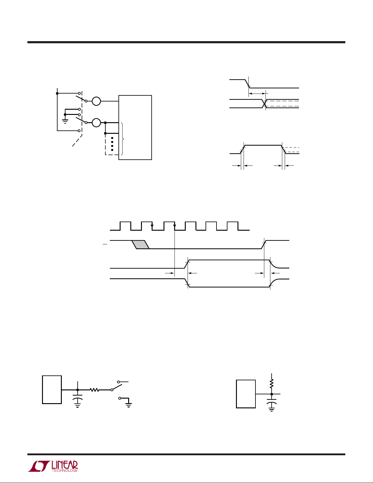
TEST CIRCUITS
LTC1090
On and Off Channel Leakage Current Voltage Waveforms for D
5V
I
ON
A
I
OFF
ON CHANNELS
SCLK 0.8V
D
OUT
A
Voltage Waveforms for D
D
OUT
t
r
dis
POLARITY
ACLK
CS
OFF
CHANNELS
LTC1090 • TC01
Voltage Waveforms for ten and t
1
2
Delay Time, t
OUT
t
dDO
Rise and Fall Times, tr, t
OUT
2.0V
2.4V
0.4V
2.4V
0.4V
t
f
LTC1090 • TC02
dDO
f
D
OUT
WAVEFORM 1
(SEE NOTE 1)
D
OUT
WAVEFORM 2
(SEE NOTE 2)
NOTE 1: WAVEFORM 1 IS FOR AN OUTPUT WITH INTERNAL CONDITIONS SUCH THAT THE OUTPUT
IS HIGH UNLESS DISABLED BY THE OUTPUT CONTROL
NOTE 2: WAVEFORM 2 IS FOR AN OUTPUT WITH INTERNAL CONDITIONS SUCH THAT THE OUTPUT
IS LOW UNLESS DISABLED BY THE OUTPUT CONTROL
Load Circuit for t
TEST
POINT
D
OUT
3k
100pF
dis
and t
en
WAVEFORM 25V
WAVEFORM 1
LTC1090 • TC04
2.4V
t
en
0.4V 10%
t
dis
Load Circuit for t
D
OUT
1.4V
90%
LTC1090 • TC03
, tr, and t
dDO
3k
TEST POINT
100pF
f
LTC1090 • TC05
1090fc
5
LTC1090
U
UU
PI FU CTIO S
# PIN FUNCTION DESCRIPTION
1-8 CH0 to CH7 Analog Inputs The analog inputs must be free of noise with respect to AGND.
9 COM Common The common pin defines the zero reference point for all single ended inputs. It must be free
of noise and is usually tied to the analog ground plane.
10 DGND Digital Ground This is the ground for the internal logic. Tie to the ground plane.
11 AGND Analog Ground AGND should be tied directly to the analog ground plane.
12 V
13,14 REF
15 CS Chip Select Input A logic low on this input enables data transfer.
16 D
17 D
18 SCLK Shift Clock This clock synchronizes the serial data transfer.
19 ACLK A/D Conversion Clock This clock controls the A/D conversion process.
20 V
–
OUT
IN
CC
–
, REF
Negative Supply Tie V– to most negative potential in the circuit. (Ground in single supply applications.)
+
Reference Inputs The reference inputs must be kept free of noise with respect to AGND.
Digital Data Output The A/D conversion result is shifted out of this output.
Data Input The A/D configuration word is shifted into this input.
Positive Supply This supply must be kept free of noise and ripple by bypassing directly to the analog ground
plane.
BLOCK DIAGRA
20
V
CC
INPUT SHIFT
17
D
CH0
CH1
CH2
CH3
CH4
CH5
CH6
CH7
COM
IN
REGISTER
1
2
3
4
5
6
7
8
9
10
DGND
W
ANALOG
INPUT
MUX
AGND
11
SAMPLE
AND HOLD
18
SCLK
OUTPUT
SHIFT
REGISTER
COMP
10-BIT
SAR
10-BIT
CAPACITIVE
DAC
12
–
V
REF
14
13
+
–
REF
CONTROL
AND
TIMING
16
19
15
D
OUT
ACLK
CS
LTC1090 • BD01
6
1090fc
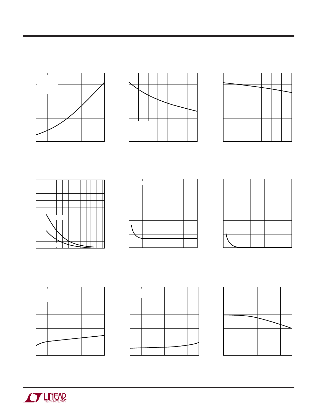
UW
AMBIENT TEMPERATURE, TA (°C)
–50
REFERENCE CURRENT, I
REF
(mA)
0.4
0.5
0.6
25 75
LTC1090 • TPC03
0.3
0.2
–25 0
50 100 125
0.1
0
V
REF
= 5V
TYPICAL PERFOR A CE CHARACTERISTICS
LTC1090
Supply Current vs Supply Voltage
6
REF +OPEN
ACLK = 2MHz
5
CS = V
CC
TA = 25°C
(mA)
4
CC
3
2
SUPPLY CURRENT, I
1
0
4
678
5
SUPPLY VOLTAGE, V
Unadjusted Offset Error vs
Reference Voltage
10
VCC = 5V
)
9
REF
8
7
1
1024
6
5
4
3
2
OFFSET ERROR (LSBs = • V
1
0
VOS = 1mV
VOS = 0.5mV
0.2
REFERENCE VOLTAGE, V
1.0 5.0
CC
(V)
REF
910
LTC1090 • TPC01
(V)
LTC1090 • TPC04
Supply Current vs Temperature Reference Current vs Temperature
1.4
1.2
(mA)
1.0
CC
0.8
0.6
REF +OPEN
SUPPLY CURRENT, I
ACLK = 2MHz
0.4
CS = 5V
V
= 5V
CC
0.2
–50
–25 0
AMBIENT TEMPERATURE, TA (°C)
Linearity Error vs Reference
Voltage
1.25
VCC = 5V
)
REF
1.0
1
1024
0.75
0.5
0.25
LINEARITY ERROR (LSBs = • V
0
1
0
REFERENCE VOLTAGE, V
50 100 125
25 75
3
2
REF
LTC1090 • TPC02
4
(V)
LTC1090 • TPC05
Change in Gain Error vs
Reference Voltage
)
1.25
VCC = 5V
REF
1.0
1
1024
0.75
0.5
0.25
CHANGE IN GAIN ERROR (LSBs = • V
5
0
1
0
REFERENCE VOLTAGE, V
3
2
REF
4
(V)
LTC1090 • TPC06
5
Offset Error vs Supply Voltage Linearity Error vs Supply Voltage
1.25
1.0
0.75
0.5
OFFSET ERROR (LSBs)
0.25
0
4
V
= 4V
REF
ACLK = 2MHz
= 1.25mV AT VCC = 5V
V
OS
678
5
SUPPLY VOLTAGE, V
CC
(V)
910
LTC1090 • TPC07
1.25
V
= 4V
REF
ACLK = 2MHz
1.0
0.75
0.5
LINEARITY ERROR (LSBs)
0.25
0
4
678
5
SUPPLY VOLTAGE, V
CC
(V)
910
LTC1090 • TPC08
Change in Gain Error vs Supply
Voltage
0.5
V
= 4V
REF
ACLK = 2MHz
0.25
0
– 0.25
– 0.5
CHANGE IN GAIN ERROR (LSBs)
4
678
5
SUPPLY VOLTAGE, V
CC
(V)
910
LTC1090 • TPC09
1090fc
7
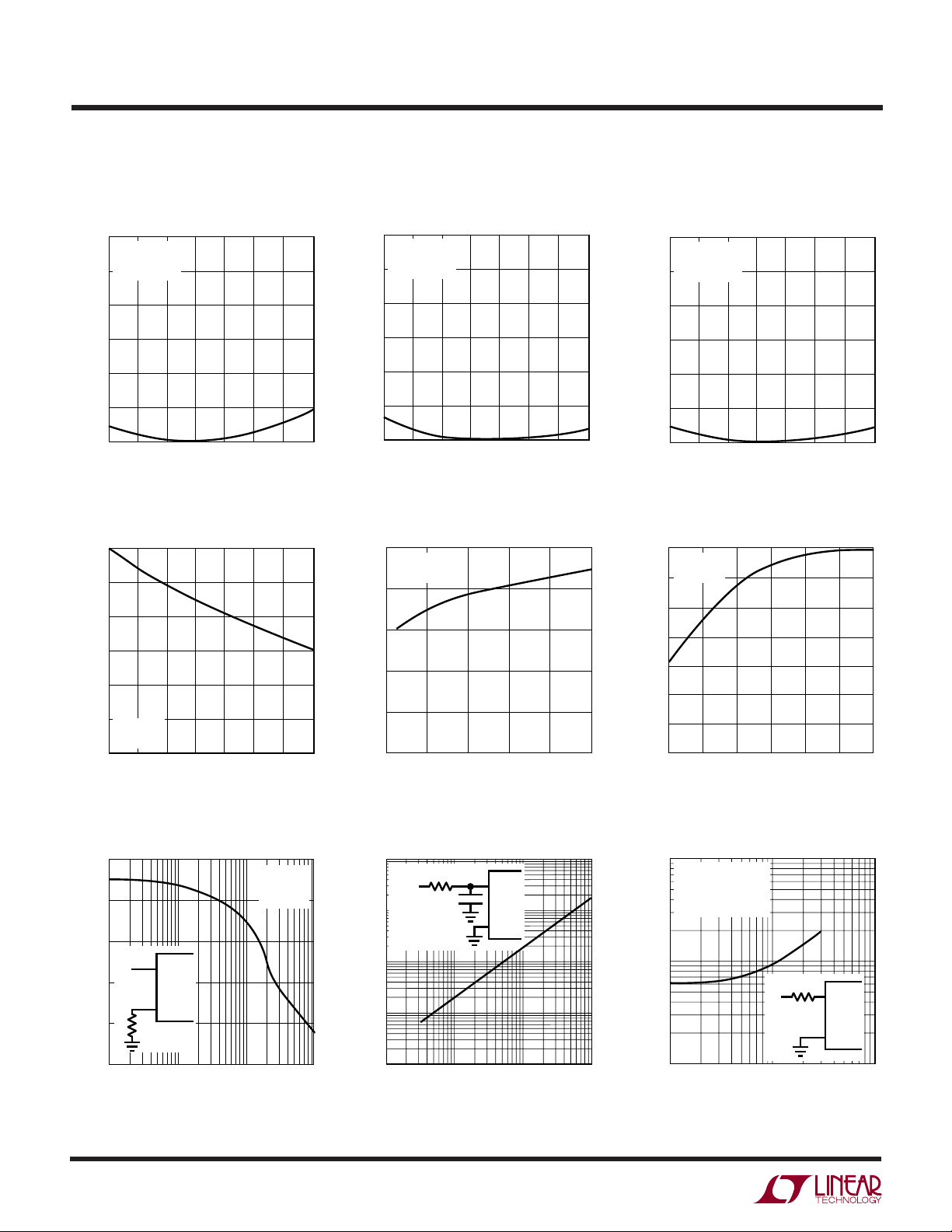
LTC1090
SUPPLY VOLTAGE, VCC (V)
4
7
6
5
4
3
2
1
0
79
LTC1090 • TPC15
56
810
MAXIMUM ACLK FREQUENCY* (MHz)
V
REF
= 4V
T
A
= 25°C
UW
TYPICAL PERFOR A CE CHARACTERISTICS
Change in Offset Error
vs Temperature
0.6
V
= 5V
CC
V
= 5V
REF
0.5
ACLK = 2MHz
0.4
0.3
0.2
0.1
0
–50
MAGNITUDE OF OFFSET CHANGE, ∆OFFSET (LSBs)
–25 0
AMBIENT TEMPERATURE, TA (°C)
Maximum Conversion Clock Rate
vs Temperature
6
5
4
3
2
1
V
= 5V
CC
MAXIMUM ACLK FREQUENCY* (MHz)
V
= 5V
REF
0
–50
–25 0
AMBIENT TEMPERATURE, TA (°C)
Maximum Conversion Clock Rate
vs Source Resistance
5
4
3
V
+
INPUT
*MAXIMUM ACLK FREQUENCY REPRESENTS THE ACLK FREQUENCY AT WHICH A 0.1LSB
SHIFT IN THE ERROR AT ANY CODE TRANSITION FROM ITS 2MHz VALVE IS FIRST DETECTED.
8
IN
2
–
1
MAXIMUM ACLK FREQUENCY* (MHz)
0
10
INPUT
R
SOURCE
100 1k 10k
50 100 125
25 75
LTC1090 • TPC10
50 100 125
25 75
LTC1090 • TPC13
VCC = 5V
V
= 5V
REF
T
= 25°C
A
–
–
R
(Ω)
SOURCE
LTC1090 • TPC16
Change in Linearity Error
vs Temperature
0.6
V
= 5V
CC
V
= 5V
REF
0.5
ACLK = 2MHz
0.4
0.3
0.2
0.1
0
MAGNITUDE OF LINEARITY CHANGE, ∆LINEARITY (LSBs)
–50
–25 0
AMBIENT TEMPERATURE, TA (°C)
50 100 125
25 75
Maximum Conversion Clock Rate
vs Reference Voltage
5
V
= 5V
CC
T
= 25°C
A
4
3
2
1
MAXIMUM ACLK FREQUENCY* (MHz)
0
1
0
REFERENCE VOLTAGE, V
3
2
Maximum Filter Resistor vs Cycle
Time
100k
10k
** (Ω)
FILTER
1k
100
MAXIMUM R
10
R
FILTER
V
IN
C
≥ 1µF
FILTER
10
CYCLE TIME, t
+
_
100 1000 10k
(µs)
CYC
**MAXIMUM R
CHANGE IN FULL SCALE ERROR FROM ITS VALUE AT R
REF
Change in Gain Error
vs Temperature
0.6
V
= 5V
CC
V
= 5V
REF
0.5
ACLK = 2MHz
0.4
0.3
0.2
0.1
0
LTC1090 • TPC11
MAGNITUDE OF GAIN CHANGE, ∆GAIN (LSBs)
–50
–25 0
AMBIENT TEMPERATURE, TA (°C)
50 100 125
25 75
Maximum Conversion Clock Rate
vs Supply Voltage
4
5
(V)
LTC1090 • TPC14
Sample-and-Hold Acquisition
Time vs Source Resistance
10
V
= 5V
REF
= 5V
V
CC
T
= 25°C
A
0 TO 5V INPUT STEP
1
R
SOURCE
V
IN
S & H ACQUISITION TIME TO 0.1% (µs)
0.1
100
LTC1090 • TPC17
REPRESENTS THE FILTER RESISTOR VALVE AT WHICH A 0.1LSB SHIFT
FILTER
1k 10k
+
(Ω)
R
SOURCE
= 0 IS FIRST DETECTED.
FILTER
LTC1090 • TPC12
+
+
_
LTC1090 • TPC18
1090fc
UW
REFERENCE VOLTAGE, V
REF
(V)
0.2
PEAK-TO-PEAK NOISE ERROR (LSBs)
0.5
1.0
2.0
15
LTC1090 • TPC21
1.5
0.25
0.75
1.75
1.25
LTC1090 NOISE = 200µV PEAK-TO-PEAK
TYPICAL PERFOR A CE CHARACTERISTICS
LTC1090
Digital Input Logic Threshold vs
Supply Voltage
4
TA = 25°C
3
2
LOGIC THRESHOLD (V)
1
0
4
5678
SUPPLY VOLTAGE, VCC (V)
910
LTC1090 • TPC19
Input Channel Leakage Current
vs Temperature Noise Error vs Reference Voltage
1000
900
800
700
600
500
400
300
200
100
INPUT CHANNEL LEAKAGE CURRENT (nA)
–50
–25
AMBIENT TEMPERATURE, TA (°C)
25
0
WUUU
APPLICATIO S I FOR ATIO
The LTC1090 is a data acquisition component which
contains the following functional blocks:
1. 10-bit successive approximation capacitive
A/D converter
2. Analog multiplexer (MUX)
3. Sample and hold (S/H)
4. Synchronous, full duplex serial interface
5. Control and timing logic
GUARANTEED
ON CHANNEL
OFF CHANNELS
50
75
100
LTC1090 • TPC20
125
DIGITAL CONSIDERATIONS
1. Serial Interface
The LTC1090 communicates with microprocessors and
other external circuitry via a synchronous, full duplex,
four wire serial interface (see Operating Sequence). The
shift clock (SCLK) synchronizes the data transfer with
each bit being transmitted on the falling SCLK edge
and captured on the rising SCLK edge in both transmitting and receiving systems. The data is transmitted and
received simultaneously (full duplex).
15810
SCLK
CS
D
D
OUT
SGL/
IN
ODD/
DIFF
SIGN
Operating Sequence
(Example: Differential Inputs (CH3 to CH2), Bipolar, MSB First and 10-Bit Word Length)
t
CYC
DON’T CARE
SEL0 UNI
SEL1
SHIFT CONFIGURATION
WORD IN
MSBF
t
SMPL
WL1 WL0
t
DON’T CARE
CONV
B9
B8 B7 B6 B5 B4 B3 B2 B1 B0
(SB)
SHIFT A/D RESULT OUT AND
NEW CONFIGURATION WORD IN
LTC1090 • AI01
1090fc
9
 Loading...