

FEATURES
■
Guaranteed
■
Guaranteed
■
Typ Offset Drift: 0.01µV/°C
■
Excellent Long Term Stability: 100nV/√Month
■
Guaranteed
■
Over Operating Temperature Range:
Guaranteed
Guaranteed
Guaranteed
■
Single Supply Operation: 4.75V to 16V
Max Offset: 5µV
Max Offset Drift: 0.05µV/°C
Max Input Bias Current: 30pA
Min Gain: 120dB
Min CMRR: 120dB
Min PSRR: 120dB
(Input Voltage Range Extends to Ground)
■
External Capacitors can be Returned to V– with No
Noise Degradation
U
APPLICATIO S
■
Thermocouple Amplifiers
■
Strain Gauge Amplifiers
■
Low Level Signal Processing
■
Medical Instrumentation
LTC1052/LTC7652
Zero-Drift
Operational Amplifier
U
DESCRIPTIO
The LTC®1052 and LTC7652 are low noise zero-drift op
amps manufactured using Linear Technology’s enhanced
LTCMOSTM silicon gate process. Chopper-stabilization
constantly corrects offset voltage errors. Both initial offset
and changes in the offset due to time, temperature and
common mode voltage are corrected. This, coupled with
picoampere input currents, gives these amplifiers
unmatched performance.
Low frequency (1/f) noise is also improved by the
chopping technique. Instead of increasing continuously
at a 3dB/octave rate, the internal chopping causes noise to
decrease at low frequencies.
The chopper circuitry is entirely internal and completely
transparent to the user. Only two external capacitors
are required to alternately sample-and-hold the offset
correction voltage and the amplified input signal. Control
circuitry is brought out on the 14-pin and 16-pin versions
to allow the sampling of the LTC1052 to be synchronized
with an external frequency source.
, LTC and LT are registered trademarks of Linear Technology Corporation.
LTCMOS is a trademark of Linear Technology Corporation.
TYPICAL APPLICATIO
Ultralow Noise, Low Drift Amplifier Noise Spectrum
5V
INPUT
3
2
0.1µF
100k
V
OS = 3µV
V
OS∆T = 50nV/°C
NOISE = 0.06µV
+
LTC1052
–
1
5V
7
6
8
4
0.1µF
3K
0.1Hz TO 10Hz
P-P
–5V
3
2
0.1µF
1
+
LT®1007
–
U
–5V
160
140
120
100
80
VOLTAGE NOISE DENSITY (nV/√Hz)
60
40
20
0
0
FREQUENCY (Hz)
400100 200 300 500
LTC1052/7652 • TA02
1052fa
68k
5V
7
4
1.5k
8
6
5V
OUTPUT
100k
100Ω
LTC1052/7652 • TA01
1
LTC1052/LTC7652
WWWU
ABSOLUTE AXI U RATI GS
(Notes 1 and 2)
Total Supply Voltage (V+ to V–) ............................... 18V
+
Input Voltage ........................ (V
+ 0.3V) to (V– – 0.3V)
Output Short Circuit Duration .......................... Indefinite
Storage Temperature Range .................. –55°C to 150°C
UU
W
PACKAGE/ORDER I FOR ATIO
TOP VIEW
C
EXTB
C
1
EXTA
2
–IN
3
+IN
METAL CAN H PACKAGE
OBSOLETE PACKAGE
ORDER PART NUMBER
8
–
+
4
–
V
+
V
/CASE
7
OUTPUT
6
5
LTC1052 OUTPUT CLAMP
LTC7652 C
RETURN
REPLACES
Operating Temperature Range
LTC1052C/LTC7652C ..........................–40°C to 85°C
LTC1052M (OBSOLETE).....................–55°C to 125°C
Lead Temperature (Soldering, 10 sec).................. 300°C
TOP VIEW
C
EXTB
C
EXTA
NC (GUARD)
–IN
+IN
NC (GUARD)
V–
1
2
3
4
–
5
+
6
7
N PACKAGE, 14-LEAD CERDIP
T
= 110°C, θJA = 130°C/W
JMAX
J PACKAGE, 14-LEAD CERDIP
INT/EXT
14
CLK IN
13
12
CLK OUT
V+
11
OUTPUT
10
OUTPUT CLAMP
9
C
RETURN
8
OBSOLETE PACKAGE
Consider the N14 Package for Alternate SourceConsider the N8 Package for Alternate Source
ORDER PART NUMBER
REPLACES
LTC7652CH
ICL7652CTV
ICL7652ITV
ICL7650CTV-1
ICL7650ITV-1
LTC1052CH
ICL7650CTV
ICL7650ITV
LTC1052MH
C
EXTA
–
IN
+N
–
V
T
J8 PACKAGE, 8-LEAD CERDIP
TOP VIEW
1
–
2
3
+
4
N8 PACKAGE
8-LEAD PDIP
= 110°C, θJA = 150°C/W
JMAX
ICL7650MTV
C
EXTB
8
+
V
7
6
OUTPUT
OUTPUT
5
CLAMP
OBSOLETE PACKAGE
Consider the N8 Package for Alternate Source
ORDER PART NUMBER
LTC1052CN8
LTC1052CJ8
LTC1052MJ8
Consult LTC Marketing for parts specified with wider operating temperature ranges.
REPLACES
ICL7650CPA
ICL7650IJA
ORDER PART NUMBER
LTC1052CN
LTC1052CJ
LTC1052MJ
C
1
EXTB
2
C
EXTA
NC (GUARD)
NC (GUARD)
3
4
–IN
5
+IN
6
7
V–
8
NC
16-LEAD PLASTIC (WIDE) SO
T
JMAX
LTC1052CSW
TOP VIEW
16
15
14
13
12
11
10
SW PACKAGE
= 110°C, θJA = 150°C/W
ICL7652CPD
ICL7650CPD
ICL7652IJD
ICL7650IJD
ICL7650MJD
INT/EXT
CLK IN
CLK OUT
V+
OUTPUT
OUTPUT CLAMP
C
RETURN
9
NC
REPLACES
LTC1052CS
1052fa
2
LTC1052/LTC7652
ELECTRICAL CHARACTERISTICS
The ● denotes the specifications which apply over the full operating
temperature range, otherwise specifications are at TA = 25°C. VS = ±5V, test circuit TC1, unless otherwise noted.
LTC1052M LTC1052C/LTC7652C
SYMBOL PARAMETER CONDITIONS MIN TYP MAX MIN TYP MAX UNITS
V
OS
∆VOS/∆Temp Average Input Offset Drift (Note 3) ● ± 0.01 ±0.05 ±0.01 ±0.05 µV/°C
∆VOS/∆Time Long-Term Offset Voltage Stability 100 100 nV/√Month
I
OS
I
B
e
nP-P
I
n
CMRR Common Mode Rejection Ratio VCM = V– to 2.7V ● 120 140 120 140 dB
PSRR Power Supply Rejection Ratio V
A
VOL
V
OUT
SR Slew Rate RL = 10k, CL = 50pF 4 4 V/µs
GBW Gain Bandwidth Product 1.2 1.2 MHz
I
S
f
S
Note 1: Absolute Maximum Ratings are those values beyond which the life
of a device may be impaired.
Note 2: Connecting any terminal to voltages greater than V
–
, may cause destructive latch-up. It is recommended that no sources
V
operating from external supplies be applied prior to power-up of the
LTC1052/LTC7652.
Note 3: These parameters are guaranteed by design. Thermocouple effects
preclude measurement of the voltage levels in high speed automatic
Input Offset Voltage (Note 3) ±0.5 ± 5 ±0.5 ± 5 µV
Input Offset Current ±30 ±90 ±30 ±90 pA
● ±2000 ±350 pA
Input Bias Current ±1 ±30 ±1 ±30 pA
● ±1000 ±175 pA
Input Noise Voltage RS = 100Ω, DC to 10HZ, TC3 1.5 1.5 µV
RS = 100Ω, DC to 1HZ, TC3 0.5 0.5 µV
P-P
P-P
Input Noise Current f = 10Hz (Note 5) 0.6 0.6 fA/√Hz
= ±2.375V to ±8V ● 120 150 120 150 dB
SUPPLY
Large-Signal Voltage Gain RL = 10k, V
= ±4V ● 120 150 120 150 dB
OUT
Maximum Output Voltage Swing RL = 10k ● ±4.7 ±4.85 ±4.7 ±4.85 V
(Note 4) R
= 100k ±4.95 ±4.95 V
L
Supply Current No Load 1.7 2.0 1.7 2.0 mA
● 3.0 3.0 mA
Internal Sampling Frequency 330 330 Hz
Clamp On Current RL = 100k ● 25 100 25 100 µA
Clamp Off Current –4V < V
< 4V 10 100 10 100 pA
OUT
+
, or less than
● 21nA
testing. V
capability. Voltages on C
is measured to a limit determined by test equipment
OS
EXTA
and C
EXTB
, A
, CMRR and PSRR are
VOL
measured to insure proper operation of the nulling loop to ensure meeting
the V
and V
OS
drift specifications. See Package-Induced VOS in the
OS
Applications Information section.
Note 4: Output clamp not connected.
Note 5: Current noise is calculated from the formula: i
q = 1.6 • 10
–19
coulomb.
n
= (2q IB)
1/2
, where
UW
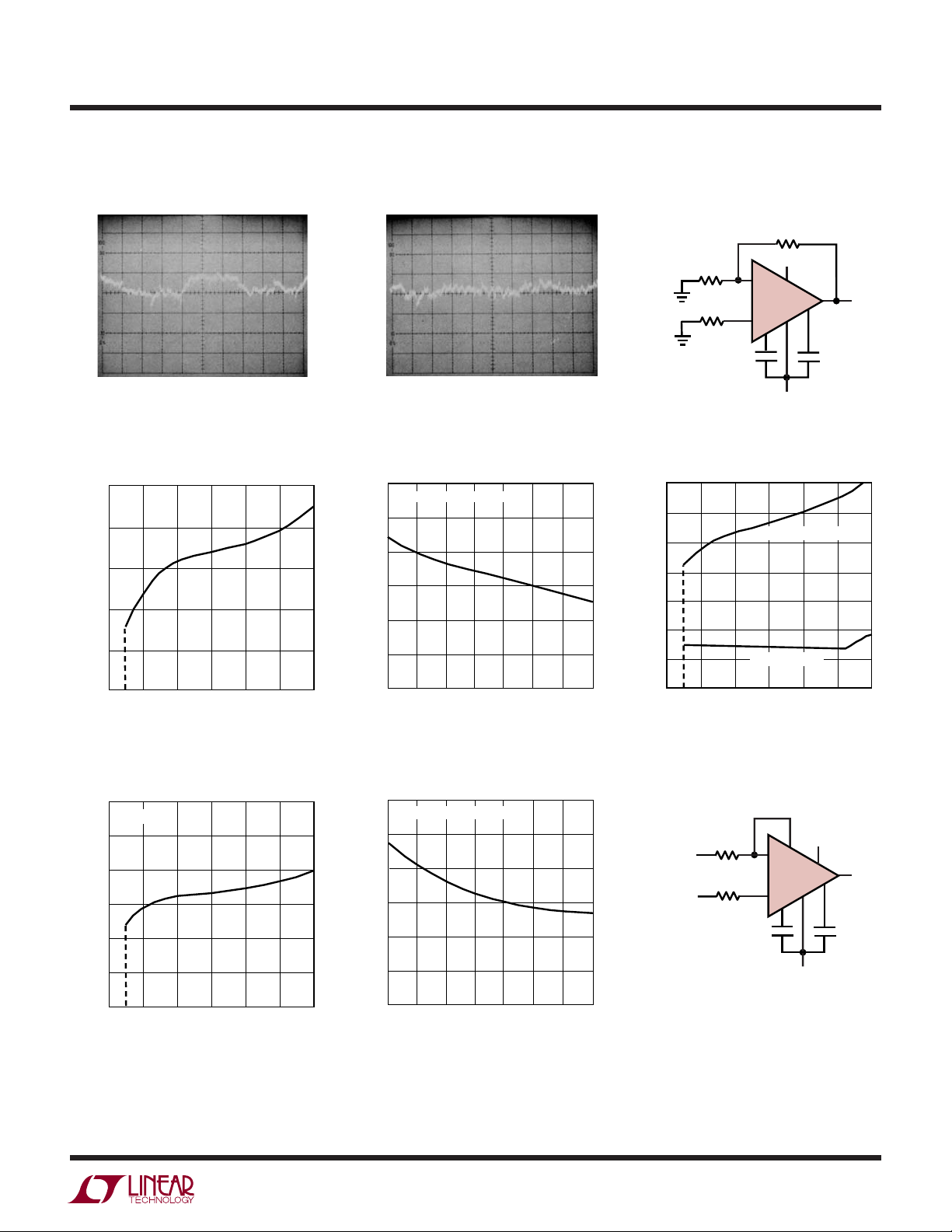
TYPICAL PERFOR A CE CHARACTERISTICS
Input Noise Voltage
5µV
0
5µV
0
10 SEC.
VS = ±5V, TEST CIRCUIT (TC3)
DC TO 1Hz
DC TO 10Hz
1052fa
3
LTC1052/LTC7652
UW
TYPICAL PERFOR A CE CHARACTERISTICS
Offset Voltage vs Sampling
Frequency
12
V
SUPPLY= ±5V
10
8
(µV)
6
OS
V
4
2
0
0
500 1000 1500 2000
SAMPLING FREQUENCY, fS (Hz)
Aliasing Error
VS = ±5V
AV = –1
TEST CIRCUIT TC2
(3Hz BANDWIDTH)
OUTPUT SPECTRUM (dB)
fI–f
S
50Hz/DIV
LTC1052/7652 • TPC01
f
S
1OHz
Frequency
5
4
3
2
1
10Hz PEAK-TO-PEAK NOISE (µV)
0
100
Common Mode Input Range vs
Supply Voltage
8
6
4
2
0
–2
–4
COMMON MODE RANGE (V)
f
I
–6
–8
0
Noise vs Sampling
P-P
V
SUPPLY= ± 5V
SAMPLING FREQUENCY, fS (Hz)
1
2
1k 10k
4
3
SUPPLY VOLTAGE (±V)
VCM = V
5
LTC1052/7652 • TPC02
–
6
7
Input Bias Current vs
Temperature
1000
900
800
(pA)
B
700
600
500
400
300
200
INPUT BIAS CURRENT, I
100
0
–50
0
–25
AMBIENT TEMPERATURE, TA(°C)
GUARANTEED
25
50
GUARANTEED
75
100
LTC1052/7652 • TPC03
125
Overload Recovery
(Output Clamp Not Used)
VS = ±5V
IV/DIV
OVERDRIVE
REMOVED
AV = –100
8
50ms/DIV
LTC1052/7652 • TPC04
Small-Signal Transient Response* Gain Phase vs Frequency
OUTPUT VOLTAGE (20mV/DIV)
AV = 1
RL = 10k
CL = 100pF
VS = ±5V
*RESPONSE IS NOT DEPENDENT ON PHASE OF CLOCK
2µs/DIV
Large-Signal Transient Response*
OUTPUT VOLTAGE (2mV/DIV)
AV = 1
RL = 10k
CL = 100pF
VS = ±5V
2µs/DIV
120
100
80
60
40
20
VOLTAGE GAIN (dB)
0
–20
–40
100 10
3
10
GAIN
4
FREQUENCY (Hz)
4
10
PHASE
5
VS= ±5V
= 100pF
C
L
6
10
LTC1052/LTC7652 • TPC06
60
80
PHASE SHIFT (DEGREES)
100
120
140
160
180
200
220
7
10
1052fa
UW
0.1µF
0.1µF
1k
V
REF
*
3
2
7
6
8
4
1
–5V
1k
5V
+
–
LTC1052
LTC1052/7652 • TPC13
V
IN
* – 5V ≤ V
REF
≤ 2.7V
5
TYPICAL PERFOR A CE CHARACTERISTICS
LTC1052/LTC7652
Broadband Noise, C
(5µV/DIV)
INPUT REFERRED NOISE
AV = –1000 1ms/DIV
EXT
= 0.1µF
Supply Current vs Supply Voltage
2.5
2.0
(mA)
S
1.5
1.0
SUPPLY CURRENT, I
0.5
0
6581012
4
TOTAL SUPPLY VOLTAGE, V+ TO V– (V)
LTC1052/LTC7652 • TPC08
14 16
Broadband Noise, C
(5µV/DIV)
INPUT REFERRED NOISE
AV = –1000 1ms/DIV
3.0
SUPPLY VOLTAGE = ± 5V
(mA)
S
2.0
1.0
SUPPLY CURRENT, I
0
–50
–25 0
AMBIENT TEMPERATURE, TA (°C)
= 1.0µF Broadband Noise Test Circuit (TC2)
EXT
50 100 125
25 75
LTC1052/LTC7652 • TPC09
R2
1M
R1
1k
R3
1k
C
EXTA
2
3
5V
–
LTC1052
+
1
–5V
Output Short-Circuit Current vs
Supply VoltageSupply Current vs Temperature
8
6
OUT (mA)
4
2
0
–10
–20
SHORT-CIRCUIT OUTPUT CURRENT, I
–30
5
4
68
TOTAL SUPPLY VOLTAGE, V+ TO V– (V)
I
SOURCE VOUT
I
SINK VOUT
10 14
7
6
8
4
C
EXTB
LTC1052/7652 • TPC07
–
= V
+
= V
12 16
LTC1052/LTC7652 • TPC10
Sampling Frequency vs Voltage Comparator Operation
600
500
(Hz)
S
400
300
200
SAMPLING FREQUENCY, f
100
0
4
TA = 25°C
5
681012
TOTAL SUPPLY VOLTAGE, V+ TO V– (V)
LTC1052/LTC7652 • TPC11
14 16
Sampling Frequency vs
Temperature
600
SUPPLY VOLTAGE = ± 5V
500
(Hz)
S
400
300
200
SAMPLING FREQUENCY, f
100
0
–50
–25 0
AMBIENT TEMPERATURE, TA (°C)
50 100 125
25 75
LT1052/LTC7652 • TPC12
1052fa
5
LTC1052/LTC7652
UW
TYPICAL PERFOR A CE CHARACTERISTICS
Response Time vs Overdrive
V
+ OVERDRIVE
REF
INPUT
{
OUTPUT
– 1mV
V
REF
10µV
5µV
20ms/DIV
{
–5V
5V
50µV
TEST CIRCUITS
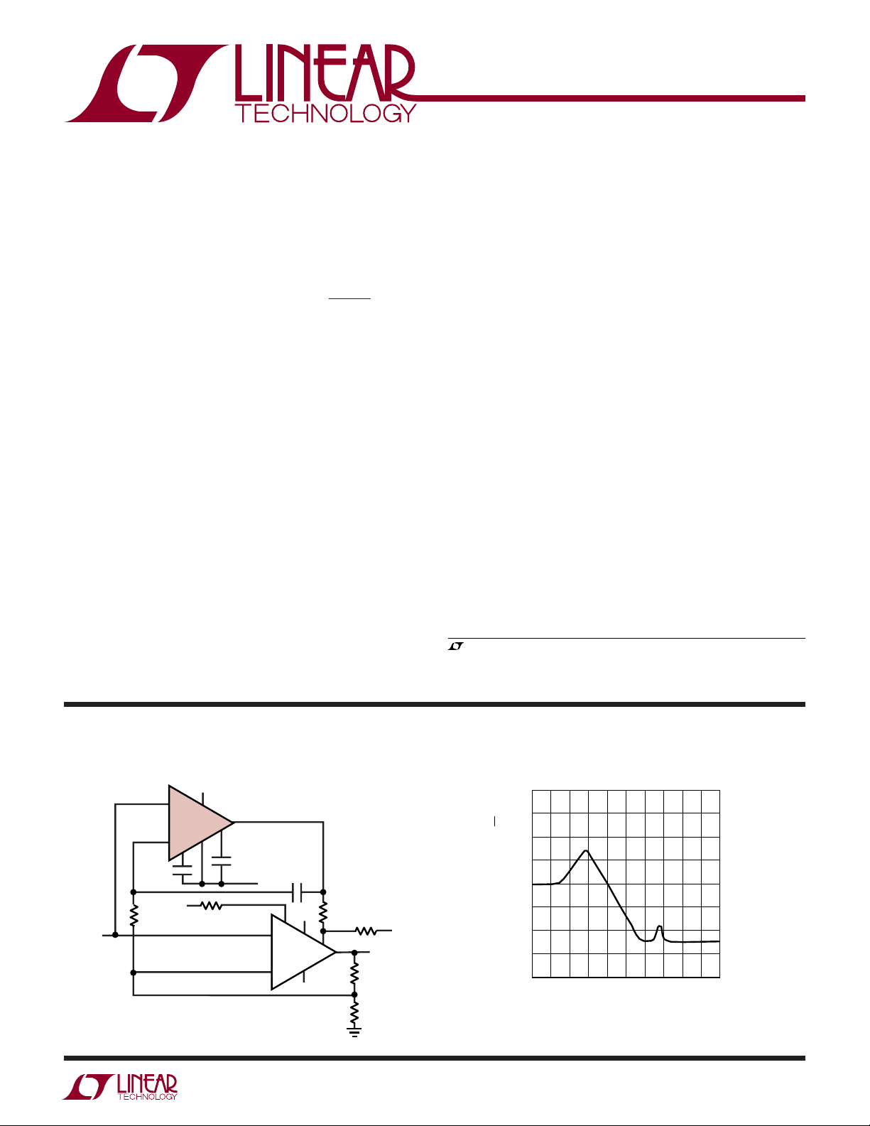
Electrical Characteristics Test Circuit (TC1) DC to 10Hz and DC to 1HZ Noise Test Circuit (TC3)
C2
R2
1M
R1
0.1µF
2
3
10Hz
1Hz
R2
–
LTC1052
+
1
V
V
+
7
4
–
16.2Ω
16.2Ω
2
3
–
LTC1052
+
1
+
V
7
6
8
4
0.1µF
–
V
OUTPUT
R
L
LTC1052/7652 • TC01
BANDWIDTH
R1
1k
0.1µF
C3
R4
R3
6
8
0.1µF
R1
R2
162k
162k
R3
16.2k
162k
3
+
C4
LT1001
2
–
34k
R4
16.2k
162k
34k
C2
0.1µF
1.0µF
6
OUTPUT
(NOISE x 20,000)
C3
1.0µF
1.0µF
C4
1.0µF
1.0µF
LTC1052/7652 • TC02
U
THEORY OF OPERATIO
DC OPERATION
The shaded portion of the LTC1052 block diagram
(Figure 1a) entirely determines the amplifier’s DC
characteristics. During the auto zero portion of the cycle,
the g
inputs are shorted together and a feedback path is
m1
closed around the input stage to null its offset. Switch S2
and capacitor C
act as a sample-and-hold to store the
EXTA
nulling voltage during the next step—the sampling cycle.
In the sampling cycle, the zeroed amplifier is used to
amplify the differential input voltage. Switch S2 connects
the amplified input voltage to C
and the output gain
EXTB
6
stage. C
and S2 act as a sample-and-hold to store the
EXTB
amplified input signal during the auto zero cycle.
By switching between these two states at a frequency
much higher than the signal frequency, a continuous
output results.
Notice that during the auto zero cycle the g
inputs are
m1
not only shorted together, but are also shorted to the
inverting input. This forces nulling with the common mode
voltage present and accounts for the extremely high
CMRR of the LTC1052. In the same fashion, variations in
1052fa
THEORY OF OPERATIO
LTC1052/LTC7652
U
power supply are also nulled. For nulling to take place, the
offset voltage, common mode voltage and power supply
must not change at a frequency which is high compared to
the frequency response of the nulling loop.
AC OPERATION AND ALIASING ERRORS
So far, the DC performance of the LTC1052 has been
explained. As the input signal frequency increases, the
problem of aliasing must be addressed. Aliasing is the
spurious formation of low and high frequency signals
caused by the mixing of the input signal with the sampling
frequency, fS. The frequency of the error signals, fE, is:
fE = fS ±f
I
where fI = input signal frequency.
Normally it is the difference frequency (fS – fI ) which is of
concern because the high frequency (fS + fI) can be easily
filtered. As the input frequency approaches the sampling
frequency, the difference frequency approaches zero and
will cause DC errors—the exact problem that the zero-drift
amplifier is meant to eliminate.
The solution is simple; filter the input so the sampling loop
never sees any frequency near the sampling frequency.
At a frequency well below the sampling frequency, the
LTC1052 forces I1 to equal I2 (see Figure 1b). This makes
δ l zero, thus the gain of the sampling loop zero at this and
higher frequencies (i.e., a low pass filter). The corner
frequency of this low pass filter is set by the output stage
pole (1/RL4 gm5 RL5 C2).
S3
V
REF
+IN
–IN
S1
+
g
m1
–
–
+
–
R
L1
g
m2
R
L2
V
g
m3
NULL
For frequencies above this pole, I2 is:
I2 = VIN gm6 •
1
• SC1
SC2
and
I1 – I2 = VIN gm1 – VIN gm6 •
The LTC1052 is very carefully designed so that gm1 = g
C1
C2
m6
and C1 = C2. Substituting these values in the above equation shows I1 – I2 = 0.
The gm6 input stage, with Cl and C2, not only filters the
input to the sampling loop, but also acts as a high
frequency path to give the LTC1052 good high frequency
response. The unity-gain cross frequencies for both the
DC path and high frequency path are identical
[f3dB =
1
(gm1/C1) =
2π
1
(gm6/C2)]
2π
thereby making the frequency response smooth and continuous while eliminating sampling noise in the output as
the loop transitions from the high gain DC loop to the high
frequency loop.
The typical curves show just how well the amplifier works.
The output spectrum shows that the difference frequency
(fI–fS = 100Hz) is down by 80dB and the frequency
response curve shows no abnormalities or perturbations.
Also note the well-behaved small and large-signal step
responses and the absence of the sampling frequency in
the output spectrum. If the dynamics of the amplifier
(i.e., slew rate and overshoot), depend on the sampling
clock, the sampling frequency will appear in the output
spectrum.
C1
C2
S2
g
m4
C
EXT B
C
EXT A
–
+
+
R
L4
g
m5
V
OUT
R
L5
–
g
m6
+
Figure 1a. LTC1052 Block Diagram
Auto Zero Cycle
V–
LTC1052/7652 • TPC13
1052fa
7
LTC1052/LTC7652
U
THEORY OF OPERATIO
S3
V
REF
l
+IN
–IN
S1
+
g
m1
–
–
g
m6
+
2
δl
–
+
–
l
1
R
L1
l
3
Figure 1b. LTC1052 Block Diagram
WUUU
APPLICATIO S I FOR ATIO
g
m2
g
m3
Sampling Cycle
C1
C2
S2
g
m4
R
L2
C
EXT B
C
EXT A
–
V
–
+
+
R
L4
g
m5
LTC1052/7652 • TO02
V
OUT
R
L5
EXTERNAL CAPACITORS
C
EXTA
and C
are the holding elements of a sample-
EXTB
and-hold circuit. The important capacitor characteristics
are leakage current and dielectric absorption. A high
quality film-type capacitor such as mylar or polypropylene
provides excellent performance. However, low grade
capacitors such as ceramic are suitable in many
applications.
Capacitors with very high dielectric absorption (ceramic)
can take several seconds to settle after power is first
turned on. This settling appears as clock ripple on the
output and, as the capacitor settles, the ripple gradually
disappears. If fast settling after power turn-on is
important, mylar or polypropylene is recommended.
Above 85°C, leakage, both from the holding capacitors
and the printed circuit board, becomes important. To
maintain the capabilities of the LTC1052 it may be
necessary to use PTFE capacitors and PTFE standoffs
when operating at 125°C (see Achieving Picoampere/
Microvolt Performance).
C
EXTA
and C
are normally in the range of 0.1µF
EXTB
to 1.0µF. All specifications are guaranteed with 0.1µF and
the broadband noise (refer to Typical Performance Characteristics) is only very slightly degraded with 0.1µF.
Output clock ripple is not present for capacitors of 0.1µF
or greater at any temperature.
On competitive devices, connecting C
EXTA
and C
EXTB
to
V– causes an increase in amplifier noise. Design changes
have eliminated this problem on the LTC1052. On the
14-pin LTC1052 and 8-pin LTC7652, the capacitors can
be returned to V– or C
RETURN
with no change in noise
performance.
ACHIEVING PICOAMPERE/MICROVOLT PERFORMANCE
Picoamperes
In order to realize the picoampere level of accuracy of the
LTC1052, proper care must be exercised. Leakage
currents in circuitry external to the amplifier can
significantly degrade performance. High quality insulation
should be used (e.g., PTFE, Kel-F); cleaning of all
insulating surfaces to remove fluxes and other residues
will probably be necessary—particularly for high
temperature performance. Surface coating may be
necessary to provide a moisture barrier in high humidity
environments.
Board leakage can be minimized by encircling the input
connections with a guard ring operated at a potential
close to that of the inputs: in inverting configurations, the
guard ring should be tied to ground; in noninverting
1052fa
8
 Loading...