

LINEAR TECHNOLOGY LTC1051, LTC1053 Technical data
FEATURES
LTC1051/LTC1053
Dual/Quad Precision
Zero-Drift Operational Amplifiers
With Internal Capacitors
U
DESCRIPTIO
■
Dual/Quad Low Cost Precision Op Amp
■
No External Components Required
■
Maximum Offset Voltage: 5µV
■
Maximum Offset Voltage Drift: 0.05µV/°C
■
Low Noise 1.5µV
■
Minimum Voltage Gain: 120dB
■
Minimum PSRR: 120dB
■
Minimum CMRR: 114dB
■
Low Supply Current: 1mA/Op Amp
■
Single Supply Operation: 4.75V to 16V
■
Input Common Mode Range Includes Ground
■
Output Swings to Ground
■
Typical Overload Recovery Time: 3ms
■
Pin Compatible with Industry Standard Dual and
(0.1Hz to 10Hz)
P-P
Quad Op Amps
U
APPLICATIO S
■
Thermocouple Amplifiers
■
Electronic Scales
■
Medical Instrumentation
■
Strain Gauge Amplifiers
■
High Resolution Data Acquisition
■
DC Accurate R C Active Filters
, LTC and LT are registered trademarks of Linear Technology Corporation.
The LTC®1051/LTC1053 are high performance, low cost
dual/quad zero-drift operational amplifiers. The unique
achievement of the LTC1051/LTC1053 is that they integrate
on chip the sample-and-hold capacitors usually required
externally by other chopper amplifiers. Further, the
LTC1051/LTC1053 offer better combined overall DC and
AC performance than is available from other chopper
stabilized amplifiers with or without internal sample/hold
capacitors.
The LTC1051/LTC1053 have an offset voltage of 0.5µV,
drift of 0.01µV/°C, DC to 10Hz, input noise voltage typically
1.5µV
and typical voltage gain of 140dB. The slew rate
P-P
of 4V/µs and gain bandwidth product of 2.5MHz are
achieved with only 1mA of supply current per op amp.
Overload recover times from positive and negative
saturation conditions are 1.5ms and 3ms respectively,
about a 100 or more times improvement over chopper
amplifiers using external capacitors.
The LTC1051 is available in an 8-lead standard plastic
dual-in-line package as well as a 16-pin SW package. The
LTC1053 is available in a standard 14-pin plastic package
and an 18-pin SO. The LTC1051/LTC1053 are plug in
replacements for most standard dual/quad op amps with
improved performance.
U
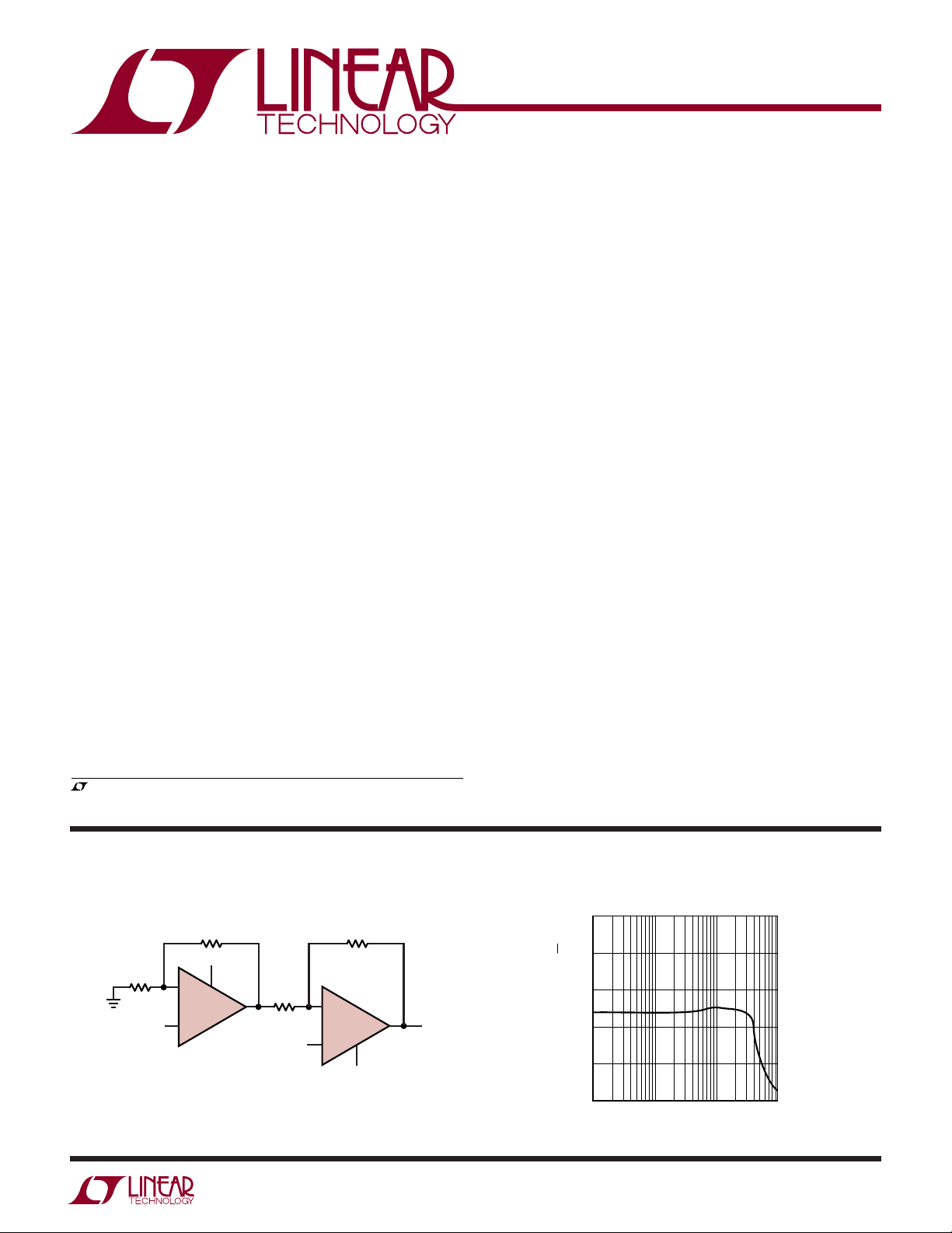
TYPICAL APPLICATIO
High Performance Low Cost Instrumentation Amplifier LTC1051 Noise Spectrum
120
6
5
–
LTC1051
+
1/2
R2
–5V
100
80
7
4
1051/53 TA01a
VOLTAGE NOISE DENSITY (nV√Hz)
60
40
20
10
100 1k 10k
FREQUENCY (Hz)
R1
5V
R2
2
8
–
1/2
LTC1051
3
V
+
IN
R1 = 499Ω, 0.1%
R2 = 100k, 0.1%
GAIN = 201
MEASURED CMRR ~ 120dB AT DC
MEASURED INPUT V
MEASURED INPUT NOISE 2µV
3µV
OS
P-P
1
(DC – 10Hz)
R1
V
IN
1051/53 TA01b
10513fa
1
LTC1051/LTC1053
WWWU
ABSOLUTE AXI U RATI GS
(Note 1)
Total Supply Voltage (V+ to V–) ............................ 16.5V
Input Voltage ........................ (V+ + 0.3V) to (V– – 0.3V)
Output Short-Circuit Duration .......................... Indefinite
Operating Temperature Range
LTC1051M, LTC1051AM
LTC1051C/LTC1053C ......................... – 40°C to 85°C
Storage Temperature Range ................. –65°C to 150°C
Lead Temperature (Soldering, 10 sec)..................300°C
UU
W
PACKAGE/ORDER I FOR ATIO
TOP VIEW
OUT A
1
–IN A
2
+IN A
3
–
V
4
N8 PACKAGE
8-LEAD PDIP
T
= 150°C, θJA = 110°C/W
JMAX
J8 PACKAGE
8-LEAD CERDIP
+
V
8
OUT B
7
–IN B
6
+IN B
5
OBSOLETE PACKAGE
Consider the N8 Package as an Alternate Source
TOP VIEW
1
NC
2
NC
3
OUT A
4
–IN A
5
+IN A
–
6
V
7
NC
8
NC
SW PACKAGE
16-LEAD PLASTIC SO
T
= 150°C, θJA = 90°C/W
JMAX
Consult LTC Marketing for parts specified with wider operating temperature ranges.
16
NC
15
NC
+
14
V
13
OUT B
12
–IN B
11
+IN B
10
NC
9
NC
ORDER PART
NUMBER
LTC1051CN8
LTC1051MJ8
LTC1051CJ8
LTC1051AMJ8
LTC1051ACJ8
ORDER PART
NUMBER
LTC1051CSW LTC1053CSW
OUT A
–IN A
+IN A
+IN B
–IN B
OUT B
TOP VIEW
1
OUT A
2
–IN A
3
+IN A
+
4
V
5
+IN B
6
–IN B
7
OUT B
N PACKAGE
14-LEAD PDIP
T
= 150°C, θJA = 65°C/W
JMAX
TOP VIEW
1
NC
2
3
4
+
5
V
6
7
8
9
NC
SW PACKAGE
18-LEAD PLASTIC SO
T
= 150°C, θJA = 85°C/W
JMAX
(OBSOLETE) .. –55°C to 125°C
ORDER PART
OUT D
14
–IN D
13
+IN D
12
–
V
11
+IN C
10
–IN C
9
OUT C
8
NUMBER
LTC1053CN
ORDER PART
18
NC
17
OUT D
16
–IN D
15
+IN D
–
14
V
13
+IN C
12
–IN C
11
OUT C
10
NC
NUMBER
ELECTRICAL CHARACTERISTICS
The ● denotes the specifications which apply over the full operating
temperature range, otherwise specifications are at TA = 25°C. VS = ±5V unless otherwise noted.
LTC1051/LTC1053 LTC1051A
PARAMETER CONDITIONS MIN TYP MAX MIN TYP MAX UNITS
Input Offset Voltage ±0.5 ±5 ±0.5 ±5 µV
Average Input Offset Drift ● ±0.0 ±0.05 ±0.0 ±0.05 µV/°C
Long Term Offset Drift 50 50 nV/√Mo
Input Bias Current ±15 ±65 ±15 ±50 pA
LTC1051C/LTC1053C
● ±135 ±100 pA
Input Offset Current (All Grades) ±30 ±125 ±30 ±100 pA
● ±175 ±150 pA
Input Noise Voltage (Note 2) RS = 100Ω, DC to 10Hz 1.5 1.5 2 µV
RS = 100Ω, DC to 1Hz 0.4 0.4 µV
P-P
P-P
10513fa
2
LTC1051/LTC1053
ELECTRICAL CHARACTERISTICS
The ● denotes the specifications which apply over the full operating
temperature range, otherwise specifications are at TA = 25°C. VS = ±5V unless otherwise noted.
LTC1051/LTC1053 LTC1051A
PARAMETER CONDITIONS MIN TYP MAX MIN TYP MAX UNITS
Input Noise Current f = 10Hz 2.2 2.2 fA/√Hz
Common Mode Rejection Ratio, CMRR VCM = V
Differential CMRR VCM = V
LTC1051, LTC1053 (Note 3)
Power Supply Rejection Ratio VS = ±2.375V to ±8V ● 116 140 120 140 dB
Large Signal Voltage Gain RL = 10k, V
Maximum Output Voltage Swing RL = 10k ● ±4.5 ±4.85 ±4.7 ±4.85 V
Slew Rate RL = 10k, CL = 50pF 4 4 V/µs
Gain Bandwidth Product 2.5 2.5 MHz
Supply Current/Op Amp No Load 1 2 1 2 mA
Internal Sampling Frequency 3.3 3.3 kHz
–
to 2.7V 106 130 114 130 dB
● 100 110 dB
–
to 2.7V 112 112 dB
= ±4V ● 116 160 120 160 dB
OUT
R
= 100k ±4.5 ±4.95 ±4.95 V
L
● 2.5 2.5 mA
The ● denotes the specifications which apply over the full operating temperature range, otherwise specifications are at TA = 25°C.
VS = ±5V unless otherwise noted.VS = 5V, GND unless otherwise noted.
LTC1051A/LTC1051/LTC1053
PARAMETER CONDITIONS MIN TYP MAX UNITS
Input Offset Voltage ±0.5 ±5 µV
Input Offset Drift ±0.01 ±0.05 µV/°C
Input Bias Current ±10 ±50 pA
Input Offset Current ±20 ±80 pA
Input Noise Voltage DC to 10Hz 1.8 µV
Supply Current/Op Amp No Load ● 1.5 mA
Note 1: Absolute Maximum Ratings are those values beyond which the life
of a device may be impaired.
Note 2: For guaranteed noise specification contact LTC Marketing.
Note 3: Differential CMRR for the LTC1053 is measured between
amplifiers A and D, and amplifiers B and C.
P-P
10513fa
3

LTC1051/LTC1053
UW
TYPICAL PERFOR A CE CHARACTERISTICS
Common Mode Input Range vs
Supply Voltage
8
6
4
2
0
–2
–4
COMMON MODE RANGE (V)
–6
–8
0
12345678
SUPPLY VOLTAGE (±V)
VCM = V
–
Supply Current vs Supply Voltage
Per Op Amp
1.50
TA = 25°C
1.25
(mA)
S
1.00
0.75
0.50
SUPPLY CURRENT, I
0.25
0
4
TOTAL SUPPLY VOLTAGE V+ TO V– (V)
81012
6
1051/53 G01
14 16
1051/53 G04
Sampling Frequency vs Supply
Voltage
4.0
TA = 25°C
(kHz)
3.5
S
3.0
2.5
SAMPLING FREQUENCY, f
2.0
4
681012
TOTAL SUPPLY VOLTAGE, V+ TO V– (V)
14 16
1051/53 G02
Sampling Frequency vs
Temperature
VS = ±5V
5
(kHz)
S
4
3
2
SAMPLING FREQUENCY, f
1
–50
0
–25
AMBIENT TEMPERATURE, TA (°C)
25
Supply Current vs Temperature
Per Op Amp Gain/Phase vs Frequency
2.0
VS = ±5V
1.8
1.6
1.4
(mA)
S
1.2
1.0
0.8
0.6
SUPPLY CURRENT, I
0.4
0.2
0
–50
–25
AMBIENT TEMPERATURE, TA (°C)
0
75
100
1051/53 G05
50
25
VOLTAGE GAIN (dB)
–20
–40
125
120
100
80
60
40
20
0
100 10k 100k 10M
1k 1M
FREQUENCY (Hz)
50
75
100
1051/53 G03
VS = ±5V
= 100pF
C
L
≥ 1k
R
L
= 25°C
T
A
1051/53 G06
125
60
80
PHASE SHIFT (DEGREES)
100
120
140
160
180
200
220
Output Short-Circuit Current vs
Supply Voltage
6
(mA)
4
OUT
I
2
0
–10
–20
SHORT-CIRCUIT OUTPUT CURRENT, I
–30
4
TOTAL SUPPLY VOLTAGE, V+ TO V– (V)
SOURCE
I
SINK
81012
6
4
CMRR vs Frequency Gain/Phase vs Frequency
≥ 1k
1051/53 G09
–60
–80
PHASE SHIFT (DEGREES)
–100
–120
–140
–160
–180
–200
–220
10513fa
–
V
= V
OUT
+
V
= V
OUT
14 16
1051/53 G07
160
140
120
100
80
CMRR (dB)
60
40
VS = ±5V
20
= 25°C
T
A
AC COMMON MODE IN = 0.5V
0
1 100 1k
10 10k 100k
P-P
FREQUENCY (Hz)
1051/53 G08
120
100
80
60
40
20
VOLTAGE GAIN (dB)
0
–20
–40
100 10k 100k 10M
1k 1M
FREQUENCY (Hz)
VS = ±2.5V
C
R
T
A
= 100pF
L
L
= 25°C
UW
TYPICAL PERFOR A CE CHARACTERISTICS
LTC1051/LTC1053
INPUT
OUTPUT
Overload Recovery
400mV
0
0
–5V
AV = –100
= ±5V
V
S
LTC1051/LTC1053 DC to 10Hz Noise
VS = ±5V
= 25°C
T
A
1µV
0.5ms
1051/53 G10
1.4µV
OUTPUT
50mV
INPUT
100mV
P-P
Small Signal Transient Response Large Signal Transient Response
OUTPUT
/DIV
A
= 1, RL = 10k, CL = 100pF
V
= ±5V, TA = 25°C
V
S
2µs/DIV
1051/53 G11
2V/DIV
INPUT
6V
A
= 1, RL = 10k, CL = 100pF
V
= ±5V, TA = 25°C
V
S
2µs/DIV
1051/53 G12
1 SEC
TEST CIRCUITS
Electrical Characteristics Test Circuit DC 10Hz Noise Test Circuit
1M
+
V
1k
2
3
–
LTC1051
+
1/2
8
6
OUTPUT
4
–
V
R
L
10Ω
100k
2
–
1/2
LTC1051
3
+
FOR 1Hz NOISE BW INCREASE ALL THE CAPACITORS BY A FACTOR OF 10.
158k 316k 475k
6
0.1µF 0.01µF
475k
10 SEC
–
LT1012
+
0.01µF
TO X-Y
RECORDER
1051/53 TC01
10513fa
5
 Loading...