

Linear Technology LTC1046MJ8, LTC1046IN8, LTC1046, LTC1046CS8, LTC1046CN8 Datasheet
FEATURES
■
50mA Output Current
■
Plug-In Compatible with ICL7660/LTC1044
■
R
= 35Ω Maximum
OUT
■
300µA Maximum No Load Supply Current at 5V
■
Boost Pin (Pin 1) for Higher Switching Frequency
■
97% Minimum Open-Circuit Voltage Conversion
Efficiency
■
95% Minimum Power Conversion Efficiency
■
Wide Operating Supply Voltage Range: 1.5V to 6V
■
Easy to Use
■
Low Cost
U
APPLICATIO S
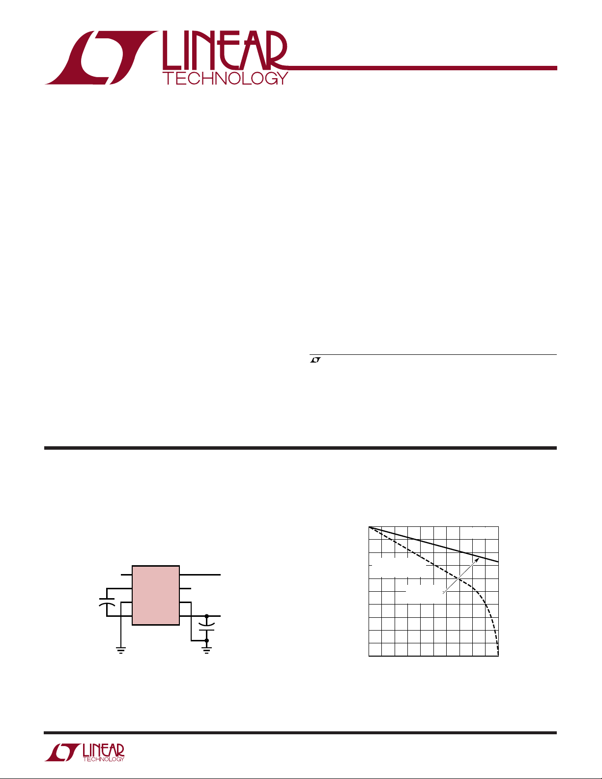
LTC1046
“Inductorless”
5V to –5V Converter
U
DESCRIPTIO
The LTC®1046 is a 50mA monolithic CMOS switched
capacitor voltage converter. It plugs in for ICL7660/
LTC1044 in 5V applications where more output current is
needed. The device is optimized to provide high current
capability for input voltages of 6V or less. It trades off
operating voltage to get higher output current. The
LTC1046 provides several voltage conversion functions:
the input voltage can be inverted (V
(V
OUT =VIN/
2) or multiplied (V
OUT
Designed to be pin-for-pin and functionally compatible
with the ICL7660 and LTC1044, the LTC1046 provides 2.5
times the output drive capability.
, LTC and LT are registered trademarks of Linear Technology Corporation.
= –VIN), divided
OUT
= ±nVIN).
■
Conversion of 5V to ±5V Supplies
■
Precise Voltage Division, V
■
Supply Splitter, V
OUT
OUT
= ±VS/2
TYPICAL APPLICATIO
Generating –5V from 5V
LTC1046
10µF
1
BOOST
2
+
+
CAP
3
GND
4
–
CAP
V
OSC
OUT
8
+
V
7
6
LV
5
= VIN/2
U
10µF
+
1046 TA01
5V INPUT
–5V INPUT
Output Voltage vs Load Current for V+ = 5V
–5
–4
ICL7660/LTC1044,
–3
–2
OUTPUT VOLTAGE (V)
–1
0
0
= 55Ω
R
OUT
R
10 20 30 40
LOAD CURRENT, IL (mA)
LTC1046,
= 27Ω
OUT
TA = 25°C
50
1046 TA02
1
LTC1046
1
2
3
4
8
7
6
5
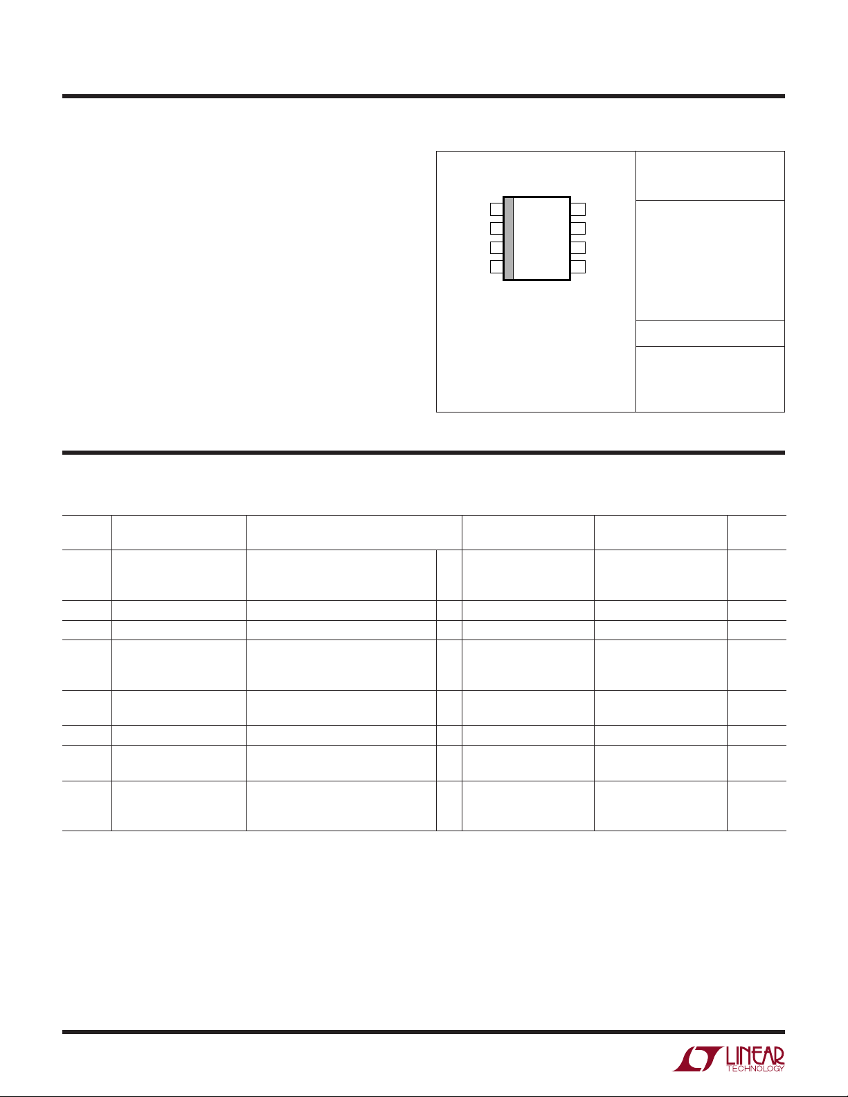
TOP VIEW
V
+
OSC
LV
V
OUT
BOOST
CAP
+
GND
CAP
–
J8 PACKAGE
8-LEAD CERDIP
N8 PACKAGE
8-LEAD PDIP
S8 PACKAGE
8-LEAD PLASTIC SO
WU
NUMBER
A
S
(Note 1)
W
O
LUTEXI TIS
A
WUW
U
ARB
G
Supply Voltage ....................................................... 6.5V
Input Voltage on Pins 1, 6 and 7
(Note 2) ............................ –0.3 < V
< (V+) +0.3V
IN
Current into Pin 6 .................................................. 20µA
Output Short Circuit Duration
(V+ ≤ 6V) ...............................................Continuous
Operating Temperature Range
LTC1046C .................................... 0°C ≤ TA ≤ 70°C
PACKAGE
/
O
RDER I FOR ATIO
ORDER PART
LTC1046CN8
LTC1046CS8
LTC1046IN8
LTC1046IS8
LTC1046MJ8
LTC1046I .................................–40°C ≤ TA ≤ 85°C
LTC1046M .................................... –55°C to 125°C
Storage Temperature Range ...............–65°C to +150°C
Lead Temperature (Soldering, 10 sec.).................300°C
LECTRICAL C CHARA TERIST
E
temperature range, otherwise specifications are at TA = 25°C. V+ = 5V, C
SYMBOL PARAMETER CONDITIONS MIN TYP MAX MIN TYP MAX UNITS
I
S
+
V
+
V
R
OUT
f
OSC
P
EFF
V
OUTEFF
I
OSC
Supply Current RL = ∞, Pins 1 and 7 No Connection 165 300 165 300 µA
= ∞, Pins 1 and 7 No Connection, 35 35 µA
R
L
V+ = 3V
Minimum Supply Voltage RL = 5kΩ ● 1.5 1.5 V
L
Maximum Supply Voltage RL = 5kΩ ● 66V
H
Output Resistance V+ = 5V, IL = 50mA (Note 3) 27 35 27 35 Ω
V+ = 2V, IL = 10mA ● 60 85 60 90 Ω
Oscillator Frequency V+ = 5V (Note 4) 20 30 20 30 kHz
V+ = 2V 4 5.5 4 5.5 kHz
Power Efficiency RL = 2.4kΩ 95 97 95 97 %
Voltage Conversion RL = ∞ 97 99.9 97 99.9 %
Efficiency
Oscillator Sink or Source V
Current Pin 1 = 0V ● 4.2 35 4.2 40 µA
= 0V or V
OSC
Pin 1 = V
ICS
+
+
The ● denotes the specifications which apply over the full operating
T
= 160°C, θJA = 100°C (J8)
JMAX
= 110°C, θJA = 130°C (N8)
T
JMAX
T
= 150°C, θJA = 150°C (S8)
JMAX
= 0pF, unless otherwise noted.
OSC
LTC1046C LTC1046I/M
● 27 45 27 50 Ω
● 15 45 15 50 µA
S8 PART MARKING
1046
1046I
U
Note 1: Absolute Maximum Ratings are those values beyond which
the life of the device may be impaired.
Note 2: Connecting any input terminal to voltages greater than V
less than ground may cause destructive latch-up. It is recommended
that no inputs from sources operating from external supplies be
applied prior to power-up of the LTC1046.
2
Note 3: R
+
or
Note 4: f
fixture capacitance loading. The 0pF frequency is correlated to this 100pF
test point, and is intended to simulate the capacitance at pin 7 when the
device is plugged into a test socket and no external capacitor is used.
is measured at TJ = 25°C immediately after power-on.
OUT
is tested with C
OSC
= 100pF to minimize the effects of test
OSC
UW
LPER
R
F
O
ATYPICA
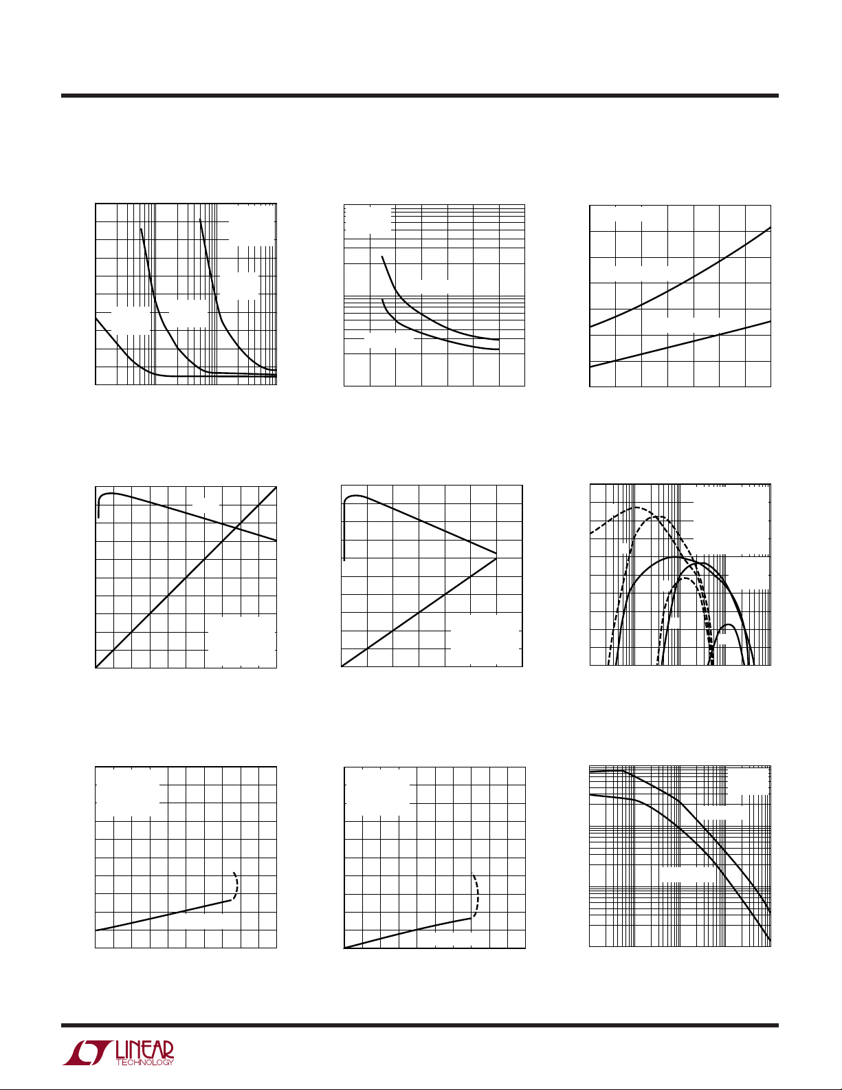
Output Resistance vs Output Resistance vs Output Resistance vs
Oscillator Frequency Supply Voltage Temperature
500
400
(Ω)
O
300
200
C1 = C2
= 100µF
100
OUTPUT RESISTANCE, R
C1 = C2
= 10µF
TA = 25°C
+
V
= 10mA
I
L
C1 = C2
= 1µF
= 5V
CCHARA TERIST
E
C
1000
TA = 25°C
= 3mA
I
L
(Ω)
O
100
C
OUTPUT RESISTANCE, R
OSC
= 0pF
ICS
(Using Test Circuit in Figure 1)
80
C1 = C2 = 10µF
70
60
V+ = 2V, C
C
= 100pF
OSC
50
40
30
OUTPUT RESISTANCE (Ω)
20
= 0pF
OSC
V+ = 5V, C
LTC1046
= 0pF
OSC
0
100
1k 10k 100k
OSCILLATOR FREQUENCY, f
OSC
(Hz)
1046 G01
10
134
0
2567
SUPPLY VOLTAGE, V+ (V)
1046 G02
10
–25 0 75
–55
AMBIENT TEMPERATURE (°C)
25 50 100 125
Power Conversion Efficiency vs Power Conversion Efficiency vs Power Conversion Efficiency vs
Load Current for V+ = 2V Load Current for V+ = 5V Oscillator Frequency
100
(%)
90
EFF
80
70
60
50
40
30
20
10
POWER CONVERSION EFFICIENCY, P
0
12 5
0
34 67
LOAD CURRENT, IL (mA)
P
EFF
I
S
TA = 25°C
+
= 2V
V
C1 = C2 = 10µF
= 8kHz
f
OSC
8910
1046 G04
100
10
(%)
9
8
7
6
5
4
3
2
1
0
90
EFF
80
SUPPLY CURRENT (mA)
70
60
50
40
30
20
10
POWER CONVERSION EFFICIENCY, P
0
10 20 50
0
P
EFF
I
S
TA = 25°C
+
= 5V
V
C1 = C2 = 10µF
f
OSC
30 40 60 70
LOAD CURRENT, IL (mA)
= 30kHz
100
90
80
70
60
50
40
30
20
10
0
1046 G05
100
(%)
98
EFF
SUPPLY CURRENT (mA)
POWER CONVERSION EFFICIENCY, P
A
96
94
92
90
88
86
84
82
80
C
100
1k 10k 100k 1M
OSCILLATOR FREQUENCY, f
B
E
D
A = 100µF, 1mA
B = 100µF, 15mA
C = 10µF, 1mA
D = 10µF, 15mA
E = 1µF, 1mA
F = 1µF, 15mA
Output Voltage vs Load Current Output Voltage vs Load Current Oscillator Frequency as a
for V+ = 2V for V+ = 5V Function of C
2.5
TA = 25°C
+
2.0
= 2V
V
= 8kHz
f
OSC
1.5
C1 = C2 = 10µF
1.0
0.5
0.0
–0.5
–1.0
OUTPUT VOLTAGE (V)
–1.5
–2.0
–2.5
2
0
4
LOAD CURRENT, IL (mA)
SLOPE = 52Ω
10 12 14 16 18 20
6
8
1046 G07
5
TA = 25°C
+
4
= 5V
V
= 30kHz
f
OSC
3
C1 = C2 = 10µF
2
1
0
–1
–2
OUTPUT VOLTAGE (V)
–3
–4
–5
0
10 20 30 40
LOAD CURRENT, IL (mA)
SLOPE = 27Ω
50 60 70 80 90 100
1046 G08
100
(kHz)
OSC
10
1
OSCILLATOR FREQUENCY, f
0.1
1
EXTERNAL CAPACITOR (PIN 7 TO GND), C
OSC
PIN 1 = V
PIN 1 = OPEN
10 100 10000
F
OSC
1000
1046 G03
V+ = 5V
= 25°C
T
A
C1 = C2
(Hz)
1046 G06
V+ = 5V
= 25°C
T
A
+
OSC
1046 G09
(pF)
3
LTC1046
LPER
100
(kHz)
OSC
UW
R
F
O
ATYPICA
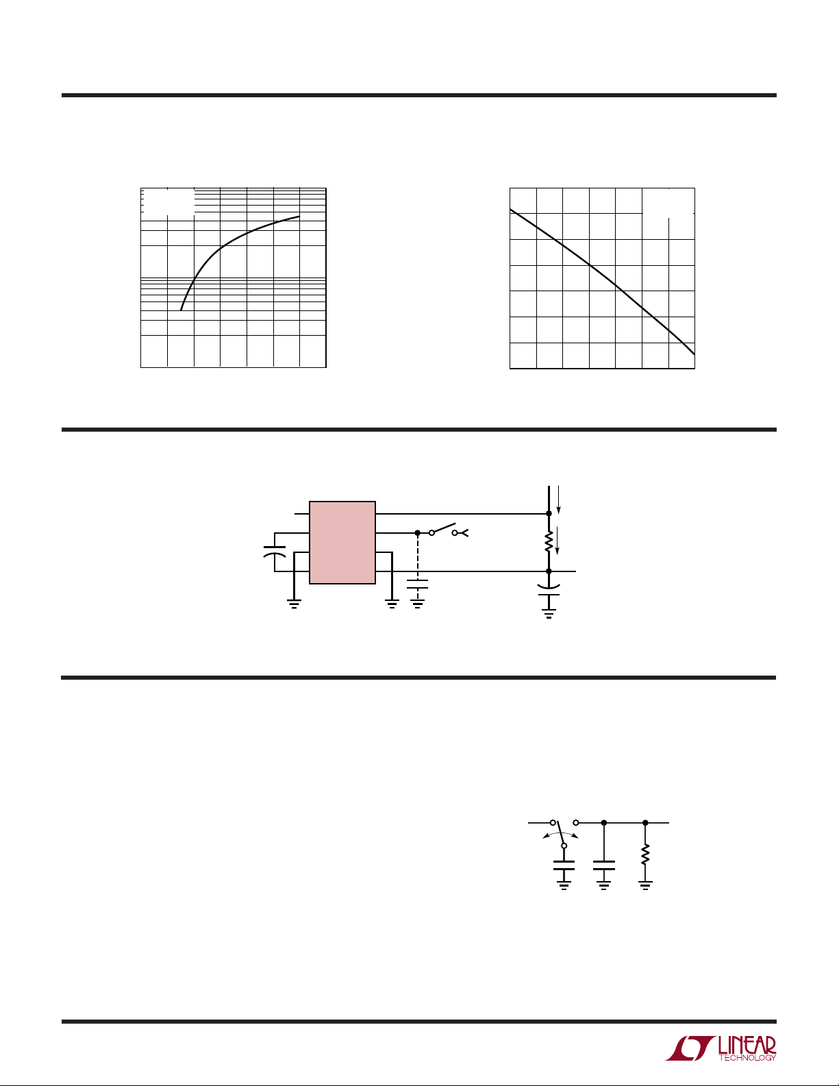
Oscillator Frequency as a Oscillator Frequency vs
Function of Supply Voltage Temperature
TA = 25°C
= 0pF
C
OSC
CCHARA TERIST
E
C
ICS
(Using Test Circuit in Figure 1)
40
38
(kHz)
OSC
36
V+ = 5V
C
OSC
= 0pF
10
OSCILLATOR FREQUENCY, f
1
0
1457
AMBIENT TEMPERATURE (°C)
TEST CIRCUIT
23 6
1046 G10
1
2
+
10µF
C1
3
4
LTC1046
BOOST
CAP
GND
CAP
34
32
30
28
OSCILLATOR FREQUENCY, f
26
–25 0 75
–55
V+ (5V)
8
+
V
V
OSC
OUT
7
6
LV
5
+
–
EXTERNAL
OSCILLATOR
C
OSC
R
L
25 50 100 125
AMBIENT TEMPERATURE (°C)
I
S
I
L
V
OUT
C2
10µF
+
1046 F01
1046 G11
Figure 1
PPLICATI
A
U
O
S
I FOR ATIO
WU
U
Theory of Operation
To understand the theory of operation of the LTC1046, a
review of a basic switched capacitor building block is
helpful.
In Figure 2, when the switch is in the left position, capacitor
C1 will charge to voltage V1. The total charge on C1 will be
q1 = C1V1. The switch then moves to the right, discharging C1 to voltage V2. After this discharge time, the charge
on C1 is q2 = C1V2. Note that charge has been transferred
from the source, V1, to the output, V2. The amount of
charge transferred is:
∆ q = q1 – q2 = C1(V1 – V2).
4
If the switch is cycled “f” times per second, the charge
transfer per unit time (i.e., current) is:
I = f • ∆q = f • C1(V1 – V2).
V2V1
f
R
C1
Figure 2. Switched Capacitor Building Block
L
C2
1046 F02
 Loading...