


查询LT3460供应商
FEATURES
■
1.3MHz Switching Frequency
■
High Output Voltage: Up to 36V
■
300mA Integrated Switch
■
12V at 70mA from 5V Input
■
5V at 60mA from 3.3V Input
■
Wide Input Range: 2.5V to 16V
■
Uses Small Surface Mount Components
■
Low Shutdown Current: <1µA
■
Low Profile (1mm) SC70 and SOT-23 (ThinSOTTM)
Packages
U
APPLICATIO S
■
Digital Cameras
■
CCD Bias Supply
■
XDSL Power Supply
■
TFT-LCD Bias Supply
■
Local 5V or 12V Supply
■
Medical Diagnostic Equipment
■
Battery Backup
LT3460
1.3MHz Step-Up DC/DC
Converter in SC70 and ThinSOT
U
DESCRIPTIO
The LT®3460 is a general purpose step-up DC/DC converter. The LT3460 switches at 1.3MHz, allowing the use
of tiny, low cost and low height capacitors and inductors.
The constant frequency results in low, predictable output
noise that is easy to filter.
The high voltage switch in the LT3460 is rated at 38V,
making the device ideal for boost converters up to 36V.
The LT3460 can generate 12V at up to 70mA from a 5V
supply.
The LT3460 is available in SC70 and SOT-23 packages.
, LTC and LT are registered trademarks of Linear Technology Corporation.
ThinSOT is a trademark of Linear Technology Corporation
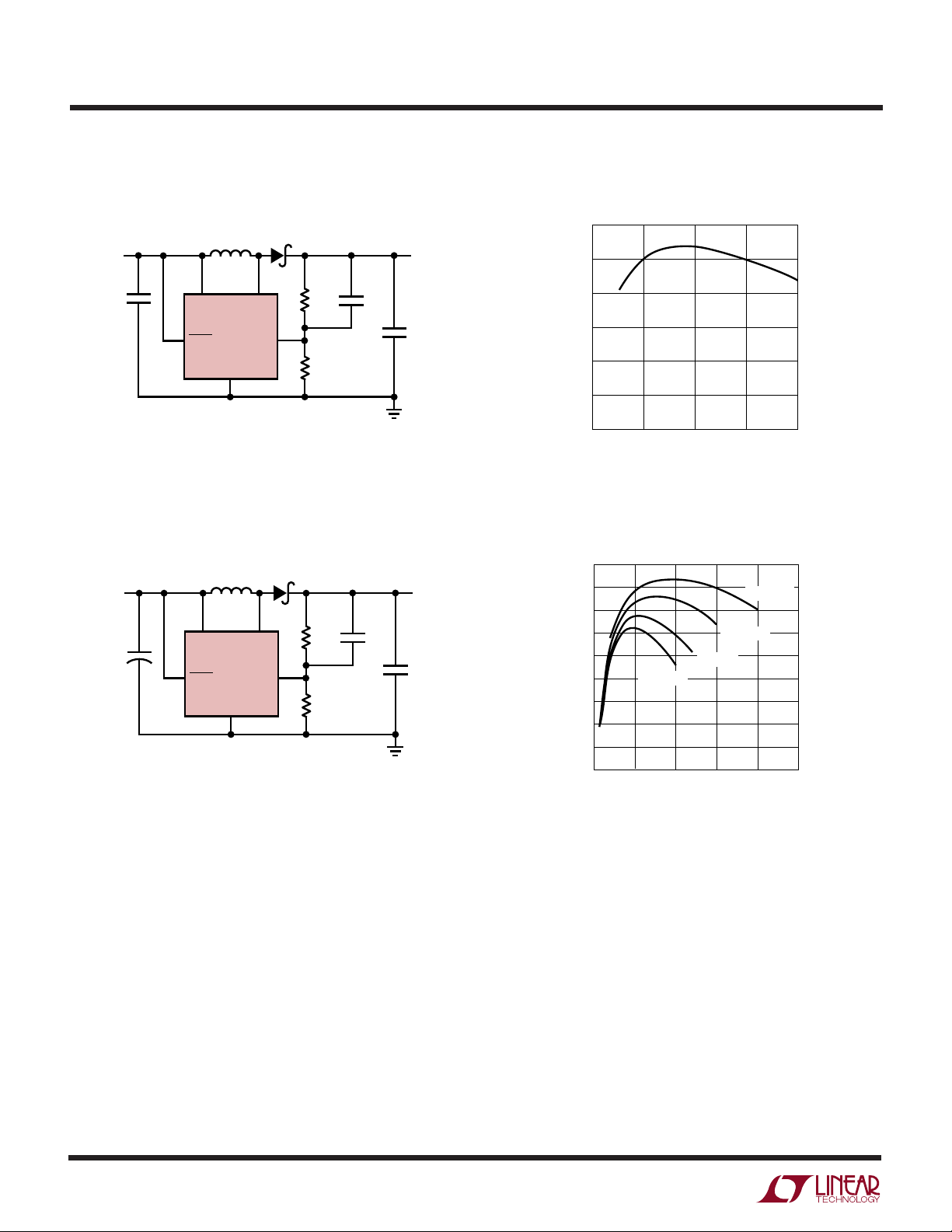
TYPICAL APPLICATIO
5V to 12V, 70mA Step-Up DC/DC Converter
V
IN
SHDN
22µH
SW
LT3460
FB
GND
V
IN
5V
4.7µF
OFF ON
U
130k
15k
22pF
V
12V
70mA
1µF
3460 F01
OUT
90
85
80
75
EFFICIENCY (%)
70
65
60
V
SW
5V/DIV
100mA/DIV
Efficiency
0
20 40 60 80
LOAD CURRENT (mA)
3460 F01a
Switching Waveforms
I
L
0.2µs/DIV
3460 F01b
3460f
1

LT3460
6 V
IN
5 GND
4 SHDN
SW 1
TOP VIEW
SC6 PACKAGE
6-LEAD PLASTIC SC70
GND 2
FB 3
WW
W
ABSOLUTE AXI U RATI GS
U
(Note 1)
Input Voltage (VIN) .................................................. 16V
SW Voltage .............................................................. 38V
FB Voltage ................................................................. 5V
SHDN Voltage .......................................................... 16V
UUW
PACKAGE/ORDER I FOR ATIO
ORDER PART
TOP VIEW
SW 1
GND 2
FB 3
S5 PACKAGE
5-LEAD PLASTIC TSOT-23
T
= 125°C, θJA = 256°C/W IN FREE AIR
JMAX
= 120°C ON BOARD OVER
θ
JA
GROUND PLANE
5 V
IN
4 SHDN
NUMBER
LT3460ES5
S5 PART MARKING
LTB1
Operating Ambient
Temperature Range (Note 2) .................. – 40°C to 85°C
Maximum Junction Temperature .......................... 125°C
Storage Temperature Range ................. –65°C to 150°C
Lead Temperature (Soldering, 10 sec)..................300°C
ORDER PART
NUMBER
LT3460ESC6
SC6 PART MARKING
T
= 125°C, θJA = 400°C/W IN FREE AIR
JMAX
θ
= 270°C/W ON BOARD OVER GROUND
JA
PLANE
LAAF
Consult LTC Marketing for parts specified with wider operating temperature ranges.
ELECTRICAL CHARACTERISTICS
temperature range, otherwise specifications are at TA = 25°C, VIN = 3V, V
PARAMETER CONDITIONS MIN TYP MAX UNITS
Minimum Operating Voltage 2.5 V
Maximum Operating Voltage 16 V
Feedback Voltage 1.235 1.255 1.275 V
Feedback Line Regulation 2.5V < VIN < 16V 0.015 %/V
FB Pin Bias Current ● 52580 nA
Supply Current 2.0 3.0 mA
Switching Frequency 1.0 1.3 1.7 MHz
Maximum Duty Cycle 85 90 %
Switch Current Limit 300 420 600 mA
Switch V
CESAT
Switch Leakage Current VSW = 5V 0.01 1 µA
SHDN Voltage High 1.5 V
SHDN Voltage Low 0.4 V
SHDN Pin Bias Current 40 µA
Note 1: Absolute Maximum Ratings are those values beyond which the life
of a device may be impaired.
The ● denotes the specifications which apply over the full operating
= 3V, unless otherwise noted.
SHDN
● 1.225 1.280 V
SHDN = 0V 0.1 0.5 µA
ISW = 250mA 320 450 mV
Note 2: The LT3460E is guaranteed to meet specifications from 0°C to
70°C. Specifications over the –40°C to 85°C operating temperature range
are assured by design, characterization and correlation with statistical
process controls.
3460f
2

TEMPERATURE (°C)
–50
250
300
350
25 75
3460 G03
200
150
100
–25 0
50 100
50
0
SHDN PIN BIAS CURRENT (µA)
400
SHDN = 3V
SHDN = 16V
UW
TYPICAL PERFOR A CE CHARACTERISTICS
LT3460
Quiescent Current
2.5
2.0
1.5
IQ (mA)
1.0
0.5
0
0
–50°C
25°C
100°C
5
10
VIN (V)
Feedback Bias Current
30
25
20
15
10
FEEDBACK BIAS CURRENT (nA)
5
15
3460 G01
Switching Frequency
1.4
1.2
1.0
0.8
0.6
0.4
SWITCHING FREQUENCY (MHz)
0.2
0
–50
–25 0
TEMPERATURE (°C)
50 100
25 75
Feedback Voltage
1.260
1.255
1.250
VFB (V)
1.245
SHDN Pin Bias Current
3460 G02
0
–50
–25 0
TEMPERATURE (°C)
50 100
25 75
3460 G04
1.240
–50
–25 0
TEMPERATURE (°C)
50 100
25 75
3460 G05
Switch Saturation Voltage
(V
) Current Limit vs Duty Cycle
CESAT
400
350
IC = 250mA
300
250
200
150
100
50
0
–50
IC = 200mA
IC = 100mA
–25 0
50 100
25 75
TEMPERATURE (°C)
3460 G06
(mV)
CESAT
V
450
400
350
300
250
200
150
CURRENT LIMIT (mA)
100
50
0
0
0.2 0.4
0.6
DUTY CYCLE
0.8 1.0
3460 G07
3460f
3

LT3460
U
PI FU CTIO S
UU
(ThinSOT/SC70 Packages)
SW (Pin 1/Pin 1): Switch Pin. Connect inductor/diode
here. Minimize trace at this pin to reduce EMI.
GND (Pin 2/Pins 2 and 5): Ground Pin. Tie directly to local
ground plane.
FB (Pin 3/Pin 3): Feedback Pin. Reference
voltage is 1.255V. Connect resistor divider tap here.
Minimize trace area at FB. Set V
V
= 1.255V (1 + R1/R2).
OUT
according to
OUT
W
BLOCK DIAGRA
R
C
C
C
∑
RAMP
1.3MHz
COMPARATOR
–
+
V
IN
(PIN 6 SC70 PACKAGE)
V
SHUTDOWN
RS, CS OPTIONAL SOFT-START COMPONENTS
R
5 1
OUT
R1 (EXTERNAL)
FB
R2 (EXTERNAL)
(EXTERNAL)
S
1.255V
REFERENCE
4
SHDN
C
(EXTERNAL)
S
+
A1
–
3
FB
GENERATOR
OSCILLATOR
SHDN (Pin 4/Pin 4): Shutdown Pin. Tie to 1.5V or higher
to enable device; 0.4V or less to disable device. Also
functions as soft-start. Use RC filter (47k, 47nF typ) as
shown in Figure 1.
V
(Pin 5/Pin 6): Input Supply Pin. Must be locally
IN
bypassed.
DRIVER
A2
R
Q
S
+
–
SW
Q1
0.1Ω
GND
2
(PINS 2 AND 5 SC70 PACKAGE)
3460 BD
Figure 1. Block Diagram
U
OPERATIO
The LT3460 uses a constant frequency, current mode
control scheme to provide excellent line and load regulation. Operation can be best understood by referring to the
block diagram in Figure 1. At the start of each oscillator
cycle, the SR latch is set, which turns on the power switch
Q1. A voltage proportional to the switch current is added
to a stabilizing ramp and the resulting sum is fed into the
positive terminal of the PWM comparator A2. When this
voltage exceeds the level at the negative input of A2, the SR
4
latch is reset turning off the power switch. The level at the
negative input of A2 is set by the error amplifier A1, and is
simply an amplified version of the difference between the
feedback voltage and the reference voltage of 1.255V. In
this manner, the error amplifier sets the correct peak
current level to keep the output in regulation. If the error
amplifier’s output increases, more current is delivered to
the output; if it decreases, less current is delivered.
3460f

OPERATIO
LT3460
U
Feedback Loop Compensation
The LT3460 has an internal feedback compensation network as shown in Figure 1 (RC and CC). However, because
the small signal characteristics of a boost converter change
with operation conditions, the internal compensation network cannot satisfy all applications. A properly designed
external feed forward capacitor from V
to FB (CF in
OUT
Figure 2) will correct the loop compensation for most
applications.
L1
V
IN
5V
C1
4.7µF
OFF ON
C1: TAIYO YUDEN X5R JMK212BJ475KG
C2: TAIYO YUDEN X5R EMK316BJ105
D1: CENTRAL SEMICONDUCTOR CMDSH2-3
L1: MURATA LQH32CN-220 OR EQUIVALENT
Figure 2. 5V to 12V Step-Up Converter
22µH
51
V
IN
LT3460
4
SHDN
GND
D1
SW
FB
2
R2
130k
3
R1
15k
C
F
22pF
V
12V
70mA
C2
1µF
3460 F02
OUT
is about 70kHz.
The feedback loop gain T(s) = K3 • GP(s) • GC(s). If it
crosses over 0dB far before fZ, the phase margin will be
small. Figure 3 is the Bode plot of the feedback loop gain
measured from the converter shown in Figure 2 without
the feedforward capacitor CF. The result agrees with
the previous discussion: Phase margin of about 20° is
insufficient.
60
50
40
30
20
10
GAIN (dB)
0
–10
–20
–30
–40
1
GAIN
PHASE
10 100 1000
FREQUENCY (kHz)
3460 F03
90
45
0
–45
–90
–135
–180
–225
–270
–315
–360
PHASE (DEG)
The LT3460 uses peak current mode control. The current
feedback makes the inductor very similar to a current
source in the medium frequency range. The power stage
transfer function in the medium frequency range can be
approximated as:
K
=
sC
•
1
,
2
G
Ps()
where C2 is the output capacitance, and K1 is a constant
based on the operating point of the converter. In continuous current mode, K1 increases as the duty cycle decreases.
The internal compensation network RC, CC can be approximated as follows in medium frequency range:
GK
Cs
()
=
•
2
••
+
CC
sC
•
C
1
sR C
The zero
f
Z
=
1
RC
π
2• • •
CC
Figure 3
In order to improve the phase margin, a feed-forward
capacitor CF in Figure 2 can be used.
Without the feed-forward capacitor, the transfer function
from V
V
FB
OUT
to FB is:
OUT
=
R
+112
RR
With the feed-forward capacitor CF, the transfer function
becomes:
V
FB
OUT
R
=
12
+
RR
1
•
s
21
••
sR C
12
•
RR
•
+
12
RR
+
F
•
C
F
+
1
The feed-forward capacitor CF generates a zero and a pole.
The zero always appears before the pole. The frequency
distance between the zero and the pole is determined only
by the ratio between V
and FB. To give maximum phase
OUT
3460f
5

LT3460
OPERATIO
U
margin, CF should be chosen so that the midpoint frequency between the zero and the pole is at the cross over
frequency.
With CF = 20pF, the feedback loop Bode plot is reshaped
as shown in Figure 4. The phase margin is about 60°.
3460 F04
90
45
0
–45
–90
–135
–180
–225
–270
–315
–360
PHASE (DEG)
60
50
40
30
20
10
GAIN (dB)
0
–10
–20
–30
–40
1
GAIN
PHASE
10 100 1000
FREQUENCY (kHz)
Figure 4.
The feed-forward capacitor increases the gain at high
frequency. The feedback loop therefore needs to have
enough attenuation at the switching frequency to reject the
switching noise. Additional internal compensation components have taken this into consideration.
For most of the applications of LT3460, the output capacitor ESR zero is at very high frequency and can be ignored.
If a low frequency ESR zero exists, for example, when a
high-ESR Tantalum capacitor is used at the output, the
phase margin may be enough even without a feed-forward
capacitor. In these cases, the feed-forward capacitor should
not be added because it may cause the feedback loop to
not have enough attenuation at the switching frequency.
Layout Hints
The high speed operation of the LT3460 demands careful
attention to board layout. You will not get advertised
performance with careless layout. Figure 5 shows the
recommended component placement.
D1 C1
V
OUT
+
C2
GND
L1
R2
R1
(SOT-23 PACKAGE)
+
V
IN
V
OUT
D1 C1
+
SHUTDOWN
C
F
C2
GND
L1
R2
R1
(SC70 PACKAGE)
+
V
IN
SHUTDOWN
C
F
3460 F05
Figure 5. Suggested Layout
6
3460f

U
TYPICAL APPLICATIO S
LT3460
5V to 12V Step-Up Converter
L1
V
IN
5V
C1
4.7µF
SHDN
C1: TAIYO YUDEN X5R JMK212BJ475
C2: TAIYO YUDEN X5R EMK212BJ105
D1: CENTRAL SEMICONDUCTOR CMDSH2-3
L1: MURATA LQH32CN-220 OR EQUIVALENT
22µH
51
V
IN
LT3460
4
SHDN
GND
D1
SW
FB
2
3
100mV/DIV
I
LOAD
130k
15k
V
OUT
58mA
34mA
22pF
V
OUT
12V
70mA
C2
1µF
3460 TA01
Load Step Response
90
85
80
75
EFFICIENCY (%)
70
65
60
0
Efficiency
20 40 60 80
LOAD CURRENT (mA)
3460 TA01a
5V to 12V with Soft-Start Circuit
L1
V
SHDN
IN
22µH
SW
LT3460
GND
V
IN
5V
C1
4.7µF
C1: TAIYO YUDEN X5R JMK212BJ475
C2: TAIYO YUDEN X5R EMK212BJ105
D1: CENTRAL SEMICONDUCTOR CMDSH2-3
L1: MURATA LQH32CN-220 OR EQUIVALENT
CONTROL
SIGNAL
47k
47nF
100µs/DIV
3460 TA01b
Input Current and Output Voltage
D1
130k
FB
15k
22pF
V
OUT
12V
70mA
C2
1µF
16V
3460 TA02
I
100mA/DIV
V
5V/DIV
CONTROL
SIGNAL
2V/DIV
IN
O
500µs/DIV
3460 TA02b
3460f
7
LT3460
LOAD CURRENT (mA)
010
20 30 40
EFFICIENCY (%)
3460 TA03a
85
80
75
70
65
60
55
U
TYPICAL APPLICATIO S
3.3V to 12V Step-Up Converter
L1
V
SHDN
22µH
IN
LT3460
GND
V
IN
3.3V
C1
4.7µF
C1: TAIYO YUDEN X5R JMK212BJ475
C2: TAIYO YUDEN X5R EMK212BJ105
D1: CENTRAL SEMICONDUCTOR CMDSH2-3
L1: MURATA LQH32CN-220 OR EQUIVALENT
D1
SW
FB
Li-Ion to 5V Step-Up Converter
L1
V
IN
SHDN
10µH
LT3460
GND
V
IN
2.7V
TO
4.2V
+
C1
4.7µF
C1: TAIYO YUDEN X5R JMK212BJ475
C2: TAIYO YUDEN X5R JMK212BJ475
D1: PHILIPS PMEG2010
L1: MURATA LQH32CN-100 OR EQUIVALENT
D1
SW
FB
130k
15k
39.2k
13k
22pF
50pF
V
OUT
12V
40mA
C2
1µF
16V
3460 TA03
V
OUT
5V
C2
4.7µF
6.3V
3460 TA07
90
88
86
84
82
80
78
EFFICIENCY (%)
76
74
72
70
0
Efficiency
Efficiency
VIN = 2.7V
50 100
LOAD CURRENT (mA)
VIN = 3.6V
VIN = 3V
150
VIN = 4.2V
200 250
3460 TA07a
8
3460f

U
TYPICAL APPLICATIO S
12V to 36V Step-Up Converter
L1
V
IN
SHDN
47µH
SW
LT3460
FB
GND
V
IN
12V
C1
1µF
16V
C1: TAIYO YUDEN X5R EMK212BJ105
C2: TAIYO YUDEN X7R UMK212BJ224
D1, D2: CENTRAL SEMICONDUCTOR CMOD4448
L1: TAIYO YUDEN LB2012
D1
D2
278k
10k
22pF
V
OUT
36V
4mA
C2
0.22µF
50V
3460 TA04
V
OUT
100mV/DIV
4mA
I
LOAD
2mA
Load Step Response
100µs/DIV
LT3460
3460 TA04a
5V to 36V Step-Up Converter
L1
V
IN
SHDN
47µH
SW
LT3460
FB
GND
V
IN
5V
C1
1µF
6.3V
C1: TAIYO YUDEN X5R JMK107BJ105
C2: TAIYO YUDEN X7R UMK212BJ224
D1, D2: CENTRAL SEMICONDUCTOR CMOD4448
L1: TAIYO YUDEN LB2012
D1
D2
278k
10k
22pF
V
OUT
36V
4mA
C2
0.22µF
50V
3460 TA05
V
OUT
100mV/DIV
4mA
I
LOAD
2mA
Load Step Response
100µs/DIV
3460 TA05a
3460f
9

LT3460
PACKAGE DESCRIPTIO
U
S5 Package
5-Lead Plastic TSOT-23
(Reference LTC DWG # 05-08-1635)
0.62
MAX
3.85 MAX
0.20 BSC
DATUM ‘A’
NOTE:
1. DIMENSIONS ARE IN MILLIMETERS
2. DRAWING NOT TO SCALE
3. DIMENSIONS ARE INCLUSIVE OF PLATING
4. DIMENSIONS ARE EXCLUSIVE OF MOLD FLASH AND METAL BURR
5. MOLD FLASH SHALL NOT EXCEED 0.254mm
6. JEDEC PACKAGE REFERENCE IS MO-193
2.62 REF
RECOMMENDED SOLDER PAD LAYOUT
PER IPC CALCULATOR
0.30 – 0.50 REF
0.95
REF
1.22 REF
1.4 MIN
0.09 – 0.20
(NOTE 3)
2.80 BSC
1.50 – 1.75
(NOTE 4)
1.00 MAX
PIN ONE
0.95 BSC
0.80 – 0.90
2.90 BSC
(NOTE 4)
0.30 – 0.45 TYP
5 PLCS (NOTE 3)
0.01 – 0.10
1.90 BSC
S5 TSOT-23 0302
10
3460f

PACKAGE DESCRIPTIO
LT3460
U
SC6 Package
6-Lead Plastic SC70
(Reference LTC DWG # 05-08-1638)
0.47
MAX
3.26 MAX
2.1 REF
RECOMMENDED SOLDER PAD LAYOUT
PER IPC CALCULATOR
0.10 – 0.40
NOTE:
1. DIMENSIONS ARE IN MILLIMETERS
2. DRAWING NOT TO SCALE
3. DIMENSIONS ARE INCLUSIVE OF PLATING
4. DIMENSIONS ARE EXCLUSIVE OF MOLD FLASH AND METAL BURR
5. MOLD FLASH SHALL NOT EXCEED 0.254mm
6. DETAILS OF THE PIN 1 INDENTIFIER ARE OPTIONAL,
BUT MUST BE LOCATED WITHIN THE INDEX AREA
7. EIAJ PACKAGE REFERENCE IS EIAJ SC-70
0.65
REF
1.16 REF
0.96 MIN
0.10 – 0.30
1.80 – 2.40
0.10 – 0.18
(NOTE 3)
1.15 – 1.35
(NOTE 4)
1.00 MAX
PIN 1
0.65 BSC
0.80 – 1.00
1.80 – 2.20
(NOTE 4)
INDEX AREA
(NOTE 6)
0.15 – 0.30
6 PLCS (NOTE 3)
0.00 – 0.10
REF
SC6 SC70 0802
Information furnished by Linear Technology Corporation is believed to be accurate and reliable.
However, no responsibility is assumed for its use. Linear Technology Corporation makes no representation that the interconnection of its circuits as described herein will not infringe on existing patent rights.
3460f
11

LT3460
LOAD CURRENT (mA)
050
100 150
EFFICIENCY (%)
3460 TA06a
80
75
70
65
60
55
50
VIN = 4V
VIN = 5V
VIN = 6.5V
TYPICAL APPLICATIO S
5V to 5V SEPIC Efficiency
SW
C3
0.22µF
FB
D1
L2
22µH
V
3V TO 10V
1µF
L1
V
IN
SHDN
22µH
LT3460
IN
C1
U
30k
50pF
V
5V
50mA
C2
1µF
OUT
GND
C1, C2: TAIYO YUDEN X5R LMK107BJ105
C3: TAIYO YUDEN X7R LMK107BJ224
D1: ON SEMICONDUCTOR MBR0520
L1, L2: MURATA LQH32CN-220 OR EQUIVALENT
10k
3460 TA06
RELATED PARTS
PART NUMBER DESCRIPTION COMMENTS
LT1613 550mA (ISW), 1.4MHz, High Efficiency Step-Up DC/DC VIN: 0.9V to 10V, V
Converter ThinSOT Package
LT1615/LT1615-1 300mA/80mA (ISW), Constant Off-Time, High Efficiency VIN: 1.2V to 15V, V
Step-Up DC/DC Converter ThinSOT Package
LT1944/LT1944-1 Dual Output 350mA/100mA (ISW), Constant Off-Time, VIN: 1.2V to 15V, V
High Efficiency Step-Up DC/DC Converter MS Package
LT1945 Dual Output, Pos/Neg, 350mA (ISW), Constant Off-Time, VIN: 1.2V to 15V, V
High Efficiency Step-Up DC/DC Converter MS Package
LT1961 1.5A (ISW), 1.25MHz, High Efficiency Step-Up DC/DC VIN: 3V to 25V, V
Converter MS8E Package
LTC3400/LTC3400B 600mA (ISW), 1.2MHz, Synchronous Step-Up DC/DC VIN: 0.85V to 5V, V
Converter ThinSOT Package
LTC3401/LTC3402 1A/2A (ISW), 3MHz, Synchronous Step-Up DC/DC Converter VIN: 0.5V to 5V, V
LT3461/LT3461A 0.3A (ISW), 1.3MHz/3MHz, High Efficiency Step-Up DC/DC VIN: 2.5V to 16V, V
Converter with Integrated Schottky SC70, ThinSOT Packages
LT3464 0.08A (ISW), High Efficiency Step-Up DC/DC Converter VIN: 2.3V to 10V, V
with Integrated Schottky, Output Disconnect ThinSOT Package
LT3465/LT3465A Constant Current, 1.2MHz/2.7MHz, High Efficiency White VIN: 2.7V to 16V, V
LED Boost Regulator with Integrated Schottky Diode ThinSOT Package
OUT(MAX)
OUT(MAX)
OUT(MAX)
OUT(MAX)
= 35V, IQ = 0.9mA, I
OUT(MAX)
OUT(MAX)
= 6V, IQ = 38µA, I
OUT(MAX)
OUT(MAX)
OUT(MAX)
OUT(MAX)
= 34V, IQ = 3mA, I
= 34V, IQ = 20µA, I
= 34V, IQ = 20µA, I
= ±34V, IQ = 20µA, I
SD
SD
SD
SD
SD
<1µA,
<1µA,
<1µA,
<6µA,
= 5V, IQ = 19µA/300µA, I
<1µA, MS Package
SD
= 38V, IQ = 2.8mA, I
= 34V, IQ = 25µA, I
= 30V, IQ = 1.9mA, I
SD
SD
<1µA,
SD
<1µA,
SD
<1µA,
<1µA,
<1µA,
12
Linear Technology Corporation
1630 McCarthy Blvd., Milpitas, CA 95035-7417
(408) 432-1900 ● FAX: (408) 434-0507
●
www.linear.com
3460f
LT/TP 0204 1K • PRINTED IN USA
LINEAR TECHNO LOGY CORPO R ATIO N 2003
 Loading...