

advertisement
2-Phase Boost Converter Delivers 10W from a
3mm × 3mm DFN Package
– Design Note 354
Jesus Rosales
Introduction
Small size, high efficiency, low noise and simplicity are
all key features for battery-powered applications and
point-of-load converters in low voltage systems. The
®
LTC
3428 is well suited for these applications because
it offers these features as well as minimum output ripple
and component count. It can start up with as little as 1.5V
and operates with inputs up to 4.5V. Its dual phase
architecture allows for an effective switching frequency
of 2MHz (1MHz/phase), which minimizes inductor and
capacitor size.
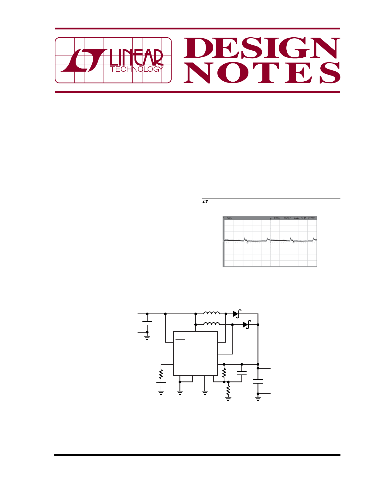
Dual Phase Converter Reduces Output Ripple
The LT3428 incorporates two internal 93mΩ, N-channel
MOSFET switches—enabling it to supply 2A of current at
5V from an input of 3.3V.
Figure 1 shows a dual phase 5V, 2A design. This converter
switches at 1MHz per phase. The two phases are 180° out
of phase, effectively doubling the output ripple frequency.
This reduces the peak-to-peak output ripple current,
which in turn makes it easier to filter out switching
frequency ripple and noise. Input ripple current is also
reduced, which minimizes stress on other components
and reduces required input capacitance. The circuit in
Figure 1 produces only 20mV
of output voltage ripple,
P–P
as shown in Figure 2.
, LTC and LT are registered trademarks of Linear Technology Corporation.
20mV/DIV
200ns/DIV
Figure 2. Output Ripple for the 5V Dual Phase Boost
Converter in Figure 1
DN354 F02
01/05/354
8
V
IN
LTC3428
PGND
L1 2µH
L2 2µH
SWB
SWA
V
OUT
GND FB
76
9
2
R4
383k
R1
127k
V
2.6V TO 4.5V
GND
IN
C2
4.7µF
6.3V
4
SHDN
5
V
C
R3
PGND
13k
C5
1nF
D1, D2: MBRM120ET
L1, L2: A920CY-2ROM
110
Figure 1. A Dual Phase, 5V at 2A Output Boost Converter
D1
D2
V
OUT
C3
47µF
6.3V
DN354 F01
5V
GND
C7
10pF
Smaller Layout is Possible by Reducing the
Number of External Components
The LTC3428 requires very few external components for
a complete boost circuit (see Figure 1). This, combined with
its 3mm × 3mm footprint and 0.75mm profile make for an
extremely compact, but feature rich converter. It can provide as much as 10W of power at 3.3V
, and includes
IN
integrated features including internal soft-start and thermal shutdown. Figure 3 shows a photo of a typical layout,
while Figure 4 shows the efficiency of this circuit at 3.3V
DN354 F03
Figure 3. Typical Layout for a
5V Dual Phase Boost Converter
90
89
88
87
86
85
84
EFFICIENCY (%)
83
82
81
80
250
750
500
LOAD CURRENT (mA)
1000
1250
1500
Figure 4. Efficiency for the 5V Dual Phase
Boost Converter in Figure 1 with 3.3V
1750
2000
DN354 F04
IN
.
IN
Antiringing Feature in Discontinuous Operation
During discontinuous mode operation, the inductor current is discharged to zero before the end of the switching
period. Once the diode is turned off, there is high frequency ringing (caused by the inductor and parasitic
capacitance) on the switch node, which can cause EMI
radiation. The LTC3428 features an antiringing circuit that
significantly reduces the discontinuous operation ringing. Figure 5 shows a switch waveform of a converter with
antiringing control and Figure 6 shows one without.
Conclusion
The LTC3428’s dual phase architecture reduces input and
output ripple when compared to a single phase design,
while providing high efficiency for up to 2A at 5V from a
3.3V input. Its 3mm × 3mm footprint and integrated
features keep the circuit layout simple and small.
1V/DIV
200ns/DIV
Figure 5. Switch Waveform for the 5V Dual Phase Boost
Converter in Discontinuous Mode with Antiringing Circuit
1V/DIV
200ns/DIV
Figure 6. Switch Waveform for a 5V Single Phase
Boost Converter in Discontinuous Mode
DN354 F05
DN354 F06
Data Sheet Download
http://www.linear.com
Linear Technology Corporation
1630 McCarthy Blvd., Milpitas, CA 95035-7417
(408) 432-1900 ● FAX: (408) 434-0507 ● www.linear.com
For applications help,
call (408) 432-1900, Ext. 2759
dn354f LT/TP 0105 409K • PRINTED IN THE USA
© LINEAR TECHNOLOGY CORPORATION 2005
 Loading...