

Linear Technology LT338A, LT138A, LM338, LM138 Datasheet
OUTPUT VOLTAGE (V)
1
0
OUTPUT VOLTAGE ERROR (%)
3
5
7
10
10 100
138A/338A TA02
1
4
6
9
12
11
8
2
2% RESISTORS
2% RESISTORS
1% RESISTORS
1% RESISTORS
LM338
LM338
LT338A
LT338A
FEATURES
■
Guaranteed
■
Guaranteed
■
Guaranteed
■
100% Thermal Limit Burn-In
■
12A Transient Output Current
1% Initial Tolerance
0.3% Load Regulation
5A Output Current
U
APPLICATIO S
■
High Power Linear Regulator
■
Battery Chargers
■
Power Driver
■
Constant-Current Regulator
LT138A/LT338A
LM138/LM338
5A Positive Adjustable
Voltage Regulator
U
DESCRIPTIO
The LT®138A series of adjustable regulators provide 5A
output current over an output voltage range of 1.2V to 32V.
The internal voltage reference is trimmed to less than 1%,
enabling a very tight output voltage. In addition to excellent line and load regulation, with full overload protection,
the LT138A incorporates new current limiting circuitry
allowing large transient load currents to be handled for
short periods. Transient load currents of up to 12A can be
supplied without limiting, eliminating the need for a large
output capacitor.
The LT138A is an improved version of the popular LM138
with improved circuit design and advanced process techniques to provide superior performance and reliability.
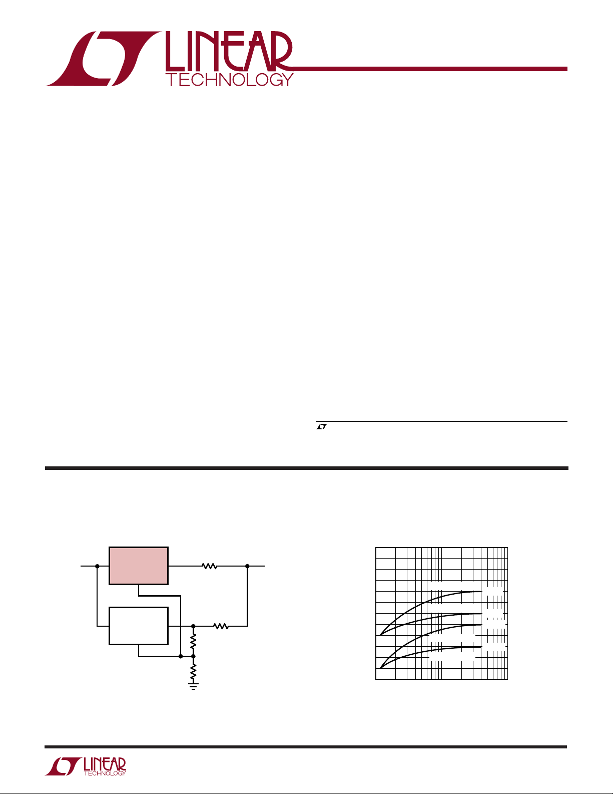
TYPICAL APPLICATIO
V
IN
THIS CIRCUIT WILL NOT WORK WITH LM VERSION DEVICES
*
CURRENT SHARING RESISTORS DEGRADE REGULATION TO 1%
**
U
Parallel Regulators for Higher Current*
LT338A
V
IN
V
IN
V
ADJ
LT350A
V
ADJ
OUT
OUT
0.01Ω**
0.016Ω**
121Ω
1%
365Ω
1%
138/338 TA01
The graph below shows the significant improvement in
output voltage tolerance achieved by using the LT138A or
LT338A.
, LTC and LT are registered trademarks of Linear Technology Corporation.
Output Voltage Error
5V
8A
1
LT138A/LT338A
LM138/LM338
A
W
O
LUTEXI TIS
S
A
WUW
U
(Note 1)
ARB
G
Power Dissipation.............................. Internally Limited
Input-to-Output Voltage Differential........................ 35V
Operating Junction Temperature Range
LT138A/LM138 ............................... –55°C to 150°C
LT338A/LM338 ................................... 0°C to 125°C
WU
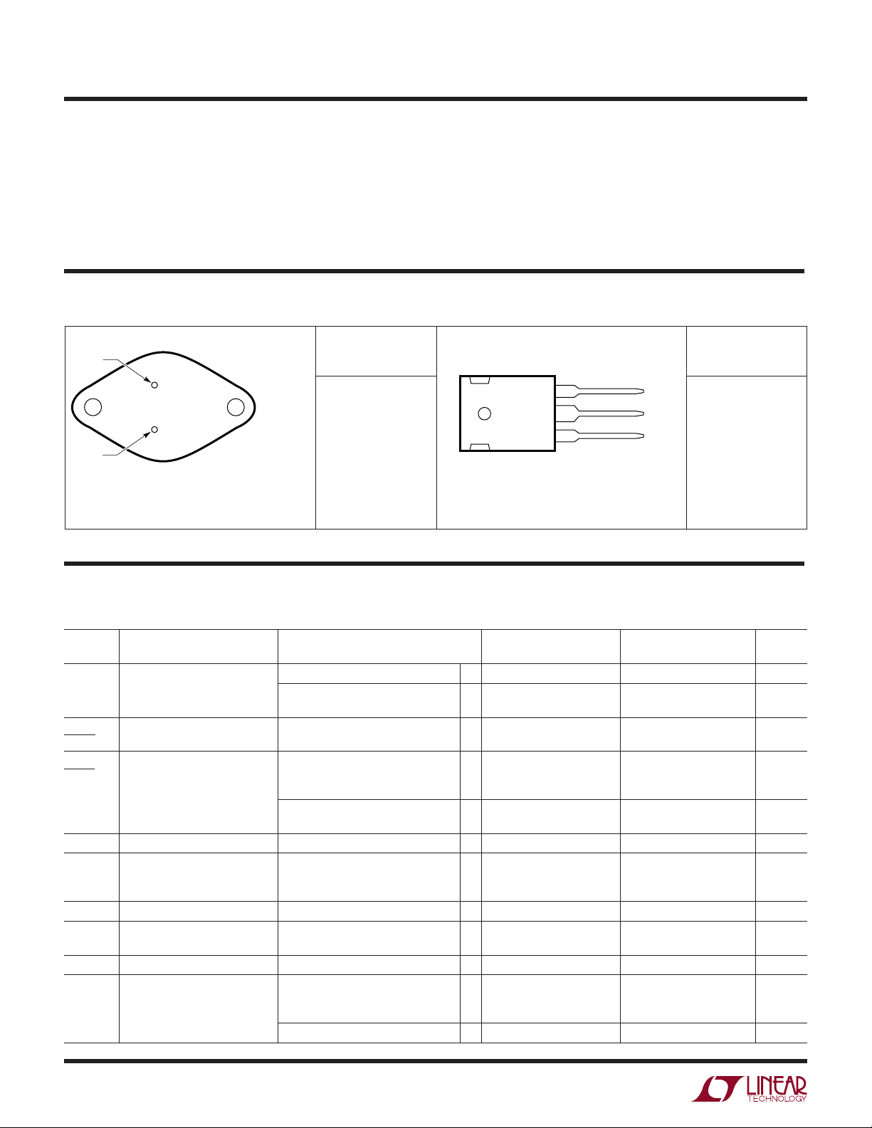
/
PACKAGE
V
IN
ADJ
2-LEAD TO-3 METAL CAN
T
= 150°C, θ
JMAX
= 125°C, θ
T
JMAX
O
BOTTOM VIEW
2
1
K PACKAGE
= 35°C/ W, θ
JA
= 35°C/ W, θ
JA
RDER I FOR ATIO
ORDER
PART NUMBER
CASE
IS OUTPUT
= 1°C/ W (LT138A/LT138)
JC
= 1°C/ W (LT338A/LT338)
JC
LT138AK
LT338AK
LM138K
LM338K
Storage Temperature Range ................ – 65°C to 150°C
Lead Temperature (Soldering, 10 sec)................. 300°C
UUU
PRECONDITIONI G
100% Thermal Limit Burn-In
U
ORDER
FRONT VIEW
3
2
1
P PACKAGE
3-LEAD PLASTIC TO-3P
T
JMAX
= 125°C, θ
= 45°C/W
JA
V
V
ADJ
PART NUMBER
OUT
IN
LM338P
Consult factory for Industrial grade parts.
ELECTRICAL CHARACTERISTICS
The ● denotes specifications which apply over the full operating
temperature range, otherwise specifications are at TA = 25°C. (Note 2)
SYMBOL PARAMETER CONDITIONS MIN TYP MAX MIN TYP MAX UNITS
V
∆V
∆V
∆V
∆I
I
ADJ
∆I
I
SC
REF
OUT
IN
OUT
OUT
ADJ
Reference Voltage I
Line Regulation 3V ≤ (VIN – V
Load Regulation 10mA ≤ I
Thermal Regulation 20ms Pulse 0.002 0.01 0.002 0.01 %/W
Ripple Rejection V
Adjust Pin Current ● 45 100 45 100 µA
Adjust Pin Current Change 10mA ≤ I
Minimum Load Current (VIN – V
Current Limit (VIN – V
= 10mA, TJ = 25°C 1.238 1.250 1.262 V
OUT
3V ≤ (VIN – V
10mA ≤ I
V
≤ 5V 5 15 5 15 mV
OUT
≥ 5V 0.1 0.3 0.1 0.3 %
V
OUT
V
≤ 5V ● 20 30 20 30 mV
OUT
≥ 5V ● 0.3 0.6 0.3 0.6 %
V
OUT
= 10V, f = 120Hz
OUT
= 0µF ● 60 60 dB
C
ADJ
= 10µF ● 60 75 60 75 dB
C
ADJ
3V ≤ (VIN – V
DC ● 58 58 A
0.5ms Peak
(VIN – V
) ≤ 35V, ● 1.225 1.250 1.270 1.19 1.24 1.29 V
OUT
≤ 5A, P ≤ 50W
OUT
) ≤ 35V, (Note 3) 0.005 0.01 0.005 0.01 %/V
OUT
≤ 5A, (Note 3)
OUT
≤ 5A, ● 0.2 5 0.2 5 µA
OUT
) ≤ 35V
OUT
) = 35V ● 3.5 5 3.5 5 mA
OUT
) ≤ 10V
OUT
) = 30V, TJ = 25°C121A
OUT
● 0.02 0.04 0.02 0.04 %/V
● 612 612 A
LT138A LM138
2
LT138A/LT338A
LM138/LM338
ELECTRICAL CHARACTERISTICS
The ● denotes specifications which apply over the full operating
temperature range, otherwise specifications are at TA = 25°C. (Note 2)
LT138A LM138
SYMBOL PARAMETER CONDITIONS MIN TYP MAX MIN TYP MAX UNITS
∆V
OUT
Temperature Stability ● 12 1 %
∆Temp
∆V
OUT
Long-Term Stability TA = 125°C, 1000 Hours 0.3 1 0.3 1 %
∆Time
e
n
θ
JC
RMS Output Noise (% of V
) 10Hz ≤ f ≤ 10kHz 0.001 0.003 %
OUT
Thermal Resistance K Package 1 1 °C/W
Junction-to-Case
The ● denotes specifications which apply over the full operating temperature range,
otherwise specifications are at TA = 25°C. (Note 2)
LT338A LM338
SYMBOL PARAMETER CONDITIONS MIN TYP MAX MIN TYP MAX UNITS
V
REF
∆V
OUT
∆V
IN
∆V
OUT
∆I
OUT
I
ADJ
∆I
ADJ
I
SC
∆V
OUT
∆Temp
∆V
OUT
∆Time
e
n
θ
JC
Reference Voltage I
Line Regulation 3V ≤ (VIN – V
Load Regulation 10mA ≤ I
= 10mA 1.238 1.250 1.262 V
OUT
3V ≤ (VIN – V
10mA ≤ I
V
≤ 5V 5 15 5 25 mV
OUT
V
≥ 5V 0.1 0.3 0.1 0.5 %
OUT
V
≤ 5V ● 20 30 20 50 mV
OUT
≥ 5V ● 0.3 0.6 0.3 1 %
V
OUT
) ≤ 35V, ● 1.225 1.250 1.270 1.19 1.24 1.29 V
OUT
≤ 5A, P ≤ 50W
OUT
) ≤ 35V, (Note 3) 0.005 0.01 0.005 0.03 %/V
OUT
≤ 5A, (Note 3)
OUT
● 0.02 0.04 0.02 0.06 %/V
Thermal Regulation 20ms Pulse 0.002 0.02 0.002 0.02 %/W
Ripple Rejection V
= 10V, f = 120Hz
OUT
C
= 0µF ● 60 60 dB
ADJ
= 10µF ● 60 75 60 75 dB
C
ADJ
Adjust Pin Current ● 45 100 45 100 µA
Adjust Pin Current Change 10mA ≤ I
3V ≤ (V
Minimum Load Current (VIN – V
Current Limit (VIN – V
DC
≤ 5A, ● 0.2 5 0.2 5 µA
OUT
– V
IN
) ≤ 35V
OUT
) = 35V ● 3.5 10 3.5 10 mA
OUT
) ≤ 10V
OUT
● 58 58 A
0.5ms Peak ● 612 612 A
(VIN – V
) = 30V, TJ = 25°C121A
OUT
Temperature Stability ● 12 1 %
Long-Term Stability TA = 125°C, 1000 Hours 0.3 1 0.3 1 %
RMS Output Noise (% of V
) 10Hz ≤ f ≤ 10kHz 0.001 0.003 %
OUT
Thermal Resistance K Package 1 1 °C/W
Junction-to-Case
Note 1: Absolute Maximum Ratings are those values beyond which the life
of the device may be impaired.
Note 2: Unless otherwise specified, these specifications apply:
V
– V
IN
= 5V and I
OUT
= 2.5A. These specifications are applicable for
OUT
power dissipations up to 50W.
Note 3: See thermal regulation specifications for changes in output voltage
due to heating effects. Load and line regulation are measured at a constant
junction temperature by low duty cycle pulse testing.
3
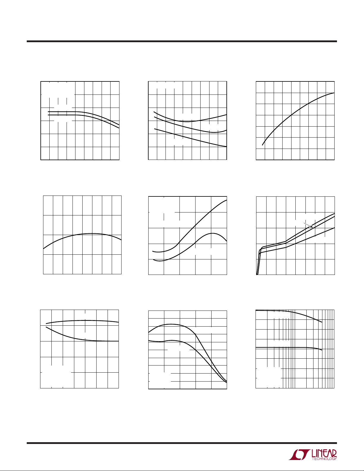
LT138A/LT338A
TEMPERATURE (°C)
–75
ADJUSTMENT CURRENT (µA)
35
40
45
75
65
138A/338A G03
30
–25 25 125
50
55
60
LM138/LM338
UW
TYPICAL PERFOR A CE CHARACTERISTICS
Load RegulationLoad Regulation
0.2
= 15V
V
IN
V
= 10V
OUT
0.1
PRELOAD = 50mA
I
0
–0.1
–0.2
–0.3
OUTPUT VOLTAGE DEVIATION (%)
–0.4
–75
= 3A
OUT
I
= 5A
OUT
–50 0
–25
TEMPERATURE (°C)
50 150
25
Temperature Stability
1.270
1.260
1.250
1.240
REFERENCE VOLTAGE (V)
Dropout Voltage
4
= 100mV
∆V
OUT
3
I
= 5A
OUT
I
= 3A
2
I
= 1A
INPUT-OUTPUT DIFFERENTIAL (V)
100
125
75
138/338 G01
1
–75
–50 0
OUT
–25
25
TEMPERATURE (°C)
50 150
OUT
100
125
75
138/338 G02
Adjustment Current
Output Impedance Minimum Operating Current
0.1
0.01
OUTPUT IMPEDANCE (Ω)
0.001
10
1
VIN = 15V
= 10V
V
OUT
I
= 500mA
OUT
= C
OUT
= 0µF
C
ADJ
= C
OUT
= 10µF
C
ADJ
5
4
3
2
QUIESCENT CURRENT (mA)
1
TJ = 25°C
= 150°C
T
J
T
= –55°C
J
1.230
–50
–25 0 25 50
TEMPERATURE (°C)
75 100 125 150
138A/338A G04
0.0001
100
10
FREQUENCY (Hz)
10k
100k
1k
1M
138/338 G05
0
0
510
15 25 40
INPUT-OUTPUT DIFFERENTIAL (V)
20
30 35
138A/338A G06
Ripple Rejection Ripple RejectionRipple Rejection
100
C
= 10µF
ADJ
80
C
= 0µF
60
40
RIPPLE REJECTION (dB)
VIN – V
20
0
OUT
I
= 500mA
OUT
f = 120Hz
= 25°C
T
J
05
ADJ
= 5V
20
15
10
OUTPUT VOLTAGE (V)
25
30
138A/338A G07
35
100
80
60
40
RIPPLE REJECTION (dB)
20
VIN = 15V
V
I
0
10
OUT
OUT
= 10V
= 0.2A
100
C
ADJ
C
ADJ
= 0µF
10k
1k
FREQUENCY (Hz)
= 10µF
100k
1M
138A/338A G08
80
70
60
RIPPLE REJECTION (dB)
50
40
V
V
f = 120Hz
T
0.1
C
= 10µF
ADJ
C
ADJ
= 15V
IN
= 10V
OUT
= 25°C
CASE
OUTPUT CURRENT (A)
= 0µF
110
138/338 G09
4
 Loading...