

Page 1
LT3023
Dual 100mA,
Low Dropout, Low Noise,
Micropower Regulator
FEATURES
n
Low Noise: 20μV
n
Low Quiescent Current: 20μA/Channel
n
Wide Input Voltage Range: 1.8V to 20V
n
Output Current: 100mA/Channel
n
Very Low Shutdown Current: <0.1μA
n
Low Dropout Voltage: 300mV at 100mA
n
Adjustable Output from 1.22V to 20V
n
Stable with 1μF Output Capacitor
n
Stable with Aluminum, Tantalum or
(10Hz to 100kHz)
RMS
Ceramic Capacitors
n
Reverse Battery Protected
n
No Reverse Current
n
No Protection Diodes Needed
n
Overcurrent and Overtemperature Protected
n
Thermally Enhanced 10-Lead MSOP and DFN
Packages
APPLICATIONS
n
Cellular Phones
n
Pagers
n
Battery-Powered Systems
n
Frequency Synthesizers
n
Wireless Modems
DESCRIPTION
The LT®3023 is a dual, micropower, low noise, low dropout regulator. With an external 0.01μF bypass capacitor,
output noise drops to 20μV
bandwidth. Designed for use in battery-powered systems,
the low 20μA quiescent current per channel makes it an
ideal choice. In shutdown, quiescent current drops to less
than 0.1μA. Shutdown control is independent for each
channel, allowing for fl exibility in power management. The
device is capable of operating over an input voltage from
1.8V to 20V, and can supply 100mA of output current from
each channel with a dropout voltage of 300mV. Quiescent
current is well controlled in dropout.
The LT3023 regulator is stable with output capacitors as
low as 1μF. Small ceramic capacitors can be used without
the series resistance required by other regulators.
Internal protection circuitry includes reverse battery
protection, current limiting, thermal limiting and reverse
current protection. The device is available as an adjustable device with a 1.22V reference voltage. The LT3023
regulator is available in the thermally enhanced 10-lead
MSOP and DFN packages.
L, LT, LTC and LTM are registered trademarks of Linear Technology Corporation. All other
trademarks are the property of their respective owners.
over a 10Hz to 100kHz
RMS
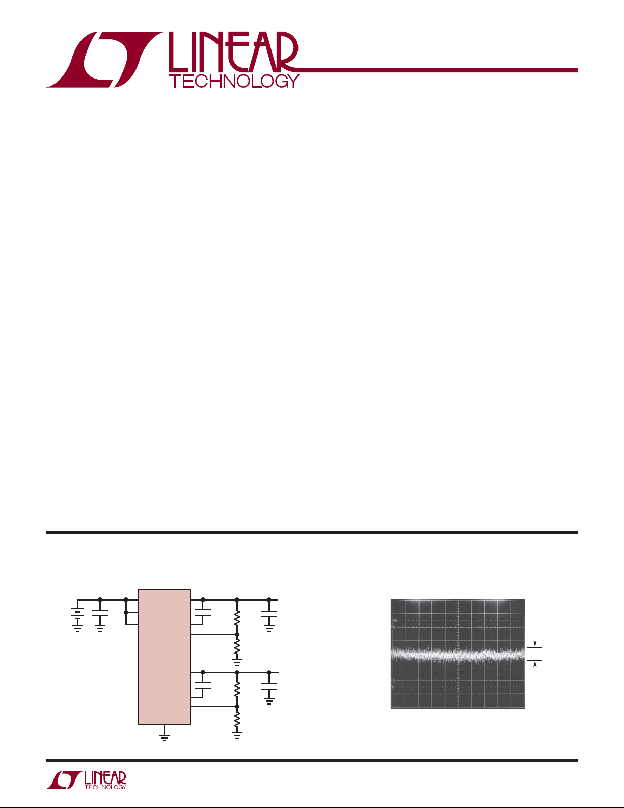
TYPICAL APPLICATION
3.3V/2.5V Low Noise Regulators
V
3.7V TO
20V
IN
1μF
IN
SHDN1
SHDN2
OUT1
BYP1
ADJ1
LT3023
OUT2
BYP2
ADJ2
GND
0.01μF
0.01μF
422k
249k
261k
249k
3.3V AT100mA
NOISE
20μV
RMS
10μF
2.5V AT100mA
NOISE
20μV
RMS
10μF
3023 TA01
V
OUT
100μV/DIV
10Hz to 100kHz Output Noise
3023 TA01b
20μV
RMS
3023fa
1
Page 2
LT3023
(
ABSOLUTE MAXIMUM RATINGS
(Note 1)
IN Pin Voltage .........................................................±20V
OUT1, OUT2 Pin Voltage .........................................±20V
Input to Output Differential Voltage .........................±20V
ADJ1, ADJ2 Pin Voltage ............................................±7V
BYP1, BYP2 Pin Voltage ........................................±0.6V
SHDN1, SHDN2 Pin Voltage ...................................±20V
PIN CONFIGURATION
TOP VIEW
10
9
8
7
6
OUT2
SHDN2
IN
SHDN1
OUT1
BYP2
1
ADJ2
2
11
3
GND
4
ADJ1
5
BYP1
10-LEAD
T
JMAX
EXPOSED PAD (PIN 11) IS GND, MUST BE SOLDERED TO PCB
DD PACKAGE
3mm s 3mm) PLASTIC DFN
= 125°C, θJA = 40°C/W, θJC = 10°C/W
ORDER INFORMATION
Output Short-Circut Duration ........................... Indefi nite
Operating Junction Temperature Range
(Note 2) .............................................–40°C to 125°C
Storage Temperature Range ................... –65°C to 150°C
Lead Temperature (Soldering, 10 sec) ..................300°C
(MSE package only)
TOP VIEW
10
1
BYP2
2
ADJ2
GND
ADJ1
BYP1
10-LEAD PLASTIC MSOP
T
= 150°C, θJA = 40°C/W, θJC = 10°C/W
JMAX
EXPOSED PAD (PIN 11) IS GND, MUST BE SOLDERED TO PCB
3
4
5
MSE PACKAGE
11
9
8
7
6
OUT2
SHDN2
IN
SHDN1
OUT1
LEAD FREE FINISH TAPE AND REEL PART MARKING* PACKAGE DESCRIPTION TEMPERATURE RANGE
LT3023EDD#PBF LT3023EDD#TRPBF LAJA
LT3023IDD#PBF LT3023IDD#TRPBF LAJA
10-Lead (3mm × 3mm) Plastic DFN
10-Lead (3mm × 3mm) Plastic DFN
–40°C to 125°C
–40°C to 125°C
LT3023EMSE#PBF LT3023EMSE#TRPBF LTAHZ 10-Lead Plastic MSOP –40°C to 125°C
LT3023IMSE#PBF LT3023IMSE#TRPBF LTAHZ 10-Lead Plastic MSOP –40°C to 125°C
LEAD BASED FINISH TAPE AND REEL PART MARKING* PACKAGE DESCRIPTION TEMPERATURE RANGE
LT3023EDD LT3023EDD#TR LAJA
LT3023IDD LT3023IDD#TR LAJA
10-Lead (3mm × 3mm) Plastic DFN
10-Lead (3mm × 3mm) Plastic DFN
–40°C to 125°C
–40°C to 125°C
LT3023EMSE LT3023EMSE#TR LTAHZ 10-Lead Plastic MSOP –40°C to 125°C
LT3023IMSE LT3023IMSE#TR LTAHZ 10-Lead Plastic MSOP –40°C to 125°C
Consult LTC Marketing for parts specifi ed with wider operating temperature ranges. *The temperature grade is identifi ed by a label on the shipping container.
For more information on lead free part marking, go to: http://www.linear.com/leadfree/
For more information on tape and reel specifi cations, go to: http://www.linear.com/tapeandreel/
ELECTRICAL CHARACTERISTICS
The l denotes the specifi cations which apply over the full operating
temperature range, otherwise specifi cations are at TA = 25°C. (Note 2)
PARAMETER CONDITIONS MIN TYP MAX UNITS
Minimum Input Voltage
(Notes 3, 11)
ADJ1, ADJ2 Pin Voltage
(Note 3, 4)
I
= 100mA
LOAD
V
= 2V, I
IN
2.3V < V
= 1mA
LOAD
< 20V, 1mA < I
IN
LOAD
< 100mA
l
1.205
l
1.190
1.8 2.3 V
1.220
1.220
1.235
1.250
3023fa
V
V
2
Page 3
LT3023
ELECTRICAL CHARACTERISTICS
The l denotes the specifi cations which apply over the full operating
temperature range, otherwise specifi cations are at T
PARAMETER CONDITIONS MIN TYP MAX UNITS
Line Regulation (Note 3) ΔV
Load Regulation (Note 3) V
Dropout Voltage
V
= V
IN
OUT(NOMINAL)
(Notes 5, 6, 11)
GND Pin Current (Per Channel)
V
= V
IN
OUT(NOMINAL)
(Notes 5, 7)
Output Voltage Noise C
ADJ1/ADJ2 Pin Bias Current (Notes 3, 8) 30 100 nA
Shutdown Threshold V
SHDN1/SHDN2 Pin Current
(Note 9)
Quiescent Current in Shutdown V
Ripple Rejection (Note 3) V
Current Limit V
Input Reverse Leakage Current V
Reverse Output Current (Notes 3,10) V
Note 1: Stresses beyond those listed under Absolute Maximum Ratings
may cause permanent damage to the device. Exposure to any Absolute
Maximum Rating condition for extended periods may affect device
reliability and lifetime.
Note 2: The LT3023 is tested and specifi ed under pulse load conditions
such that T
≅ TA. The LT3023E is 100% tested at TA = 25°C. Performance
J
at –40°C and 125°C is assured by design, characterization and correlation
with statistical process controls. The LT3023I is guaranteed over the full
–40°C to 125°C operating junction temperature range.
Note 3: The LT3023 is tested and specifi ed for these conditions with the
ADJ1/ADJ2 pin connected to the corresponding OUT1/OUT2 pin.
Note 4: Operating conditions are limited by maximum junction
temperature. The regulated output voltage specifi cation will not apply
for all possible combinations of input voltage and output current. When
operating at maximum input voltage, the output current range must be
limited. When operating at maximum output current, the input voltage
range must be limited.
Note 5: To satisfy requirements for minimum input voltage, the LT3023 is
tested and specifi ed for these conditions with an external resistor divider
(two 250k resistors) for an output voltage of 2.44V. The external resistor
divider will add a 5μA DC load on the output.
= 2V to 20V, I
IN
= 2.3V, ΔI
IN
V
= 2.3V, ΔI
IN
I
LOAD
I
LOAD
I
LOAD
I
LOAD
I
LOAD
I
LOAD
I
LOAD
I
LOAD
I
LOAD
I
LOAD
I
LOAD
I
LOAD
I
LOAD
OUT
OUT
V
OUT
V
SHDN
V
SHDN
= 6V, V
IN
= 2.72V (Avg), V
IN
I
LOAD
= 7V, V
IN
V
= 2.3V, ΔV
IN
= –20V, V
IN
OUT
LOAD
LOAD
= 1mA
= 1mA
= 10mA
= 10mA
= 50mA
= 50mA
= 100mA
= 100mA
= 0mA
= 1mA
= 10mA
= 50mA
= 100mA
= 10μF, C
= Off to On
= On to Off
= 0V
= 20V
SHDN
= 50mA
OUT
OUT
= 1.22V, VIN < 1.22V 5 10 μA
= 25°C. (Note 2)
A
= 1mA
LOAD
= 1mA to 100mA
= 1mA to 100mA
l
110 mV
11225mV
l
0.10 0.15
l
0.19
0.17 0.22
l
0.29
0.24 0.28
l
0.38
0.30 0.35
= 0.01μF, I
BYP
l
l
l
l
l
l
= 100mA, BW = 10Hz to 100kHz 20 μV
LOAD
l
l
0.25
l
l
20
55
230
1
2.2
0.8
0.65
0
1
0.45
45
100
400
2
4
1.4 V
0.5
3
= 0V (Both SHDN Pins) 0.01 0.1 μA
= 0V
OUT
RIPPLE
= –5%
= 0V
= 0.5V
P-P
, f
RIPPLE
= 120Hz,
55 65 dB
200 mA
l
110
l
1mA
Note 6: Dropout voltage is the minimum input to output voltage differential
needed to maintain regulation at a specifi ed output current. In dropout, the
output voltage will be equal to: V
Note 7: GND pin current is tested with V
IN
– V
.
DROPOUT
= 2.44V and a current source
IN
load. This means the device is tested while operating in its dropout region
or at the minimum input voltage specifi cation. This is the worst-case GND
pin current. The GND pin current will decrease slightly at higher input
voltages.
Note 8: ADJ1 and ADJ2 pin bias current fl ows into the pin.
Note 9: SHDN1 and SHDN2 pin current fl ows into the pin.
Note 10: Reverse output current is tested with the IN pin grounded and the
OUT pin forced to the rated output voltage. This current fl ows into the OUT
pin and out the GND pin.
Note 11: For the LT3023 dropout voltage will be limited by the minimum
input voltage specifi cation under some output voltage/load conditions.
See the curve of Minimum Input Voltage in the Typical Performance
Characteristics.
mV
μA
μA
μA
mA
mA
RMS
μA
μA
mA
V
V
V
V
V
V
V
V
V
3023fa
3
Page 4
LT3023
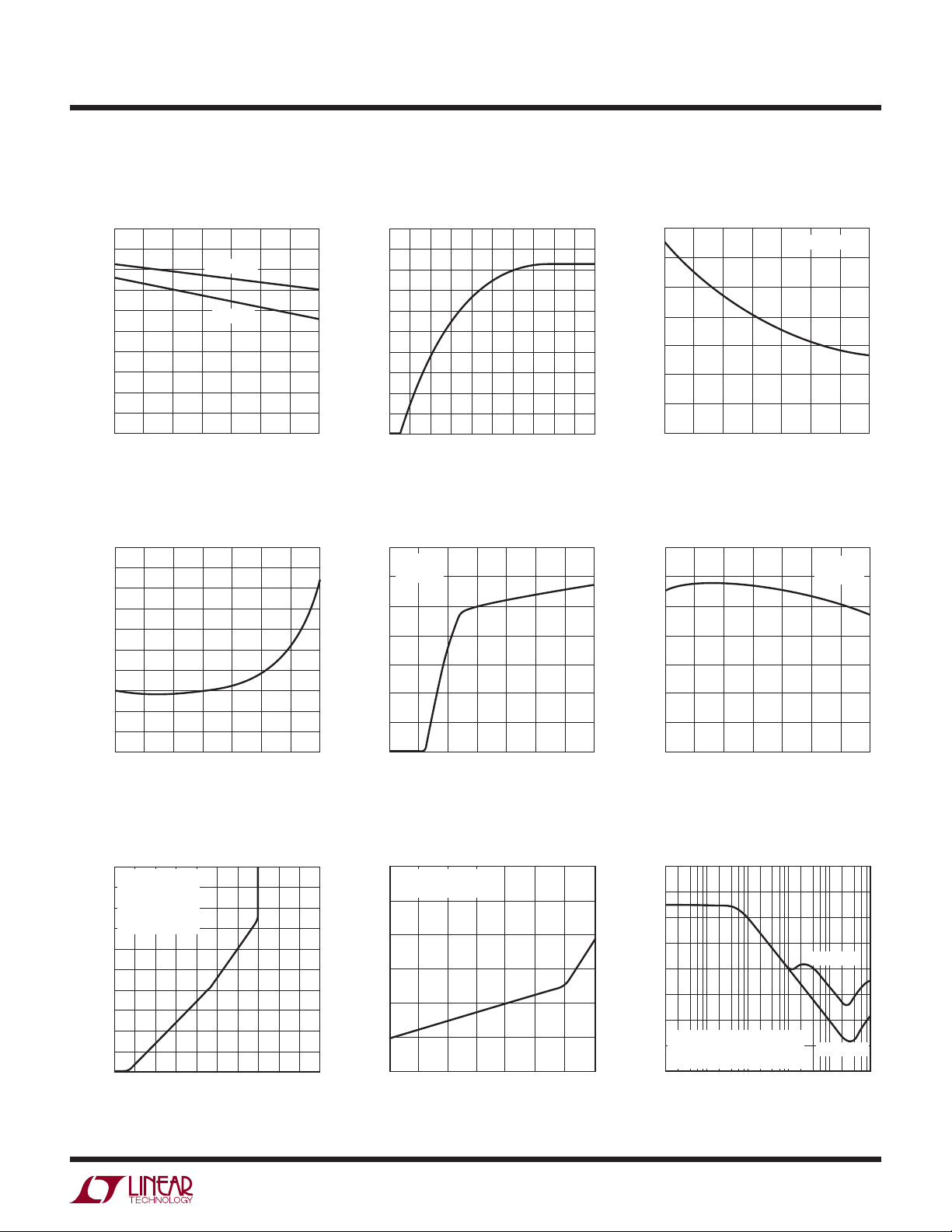
TYPICAL PERFORMANCE CHARACTERISTICS
Typical Dropout Voltage Guaranteed Dropout Voltage Dropout Voltage
500
450
400
350
300
250
200
150
DROPOUT VOLTAGE (mV)
100
50
0
0 102030
TJ = 125°C
TJ = 25°C
40
60 70 80 90 100
50
OUTPUT CURRENT (mA)
3023 G01
500
= TEST POINTS
450
400
350
300
250
200
150
DROPOUT VOLTAGE (mV)
100
50
0
0 102030
OUTPUT CURRENT (mA)
TJ ≤ 125°C
TJ ≤ 25°C
40
60 70 80 90 100
50
3023 G02
Quiescent Current ADJ1 or ADJ2 Pin Voltage Quiescent Current
40
VIN = 6V
= 250k
R
35
L
= 5μA
I
L
30
25
20
15
10
QUIESCENT CURRENT (μA)
5
0
–50
V
= V
SHDN
V
050
–25 25 75 125
TEMPERATURE (°C)
SHDN
IN
= 0V
100
3023 G03
1.240
IL = 1mA
1.235
1.230
1.225
1.220
1.215
ADJ PIN VOLTAGE (V)
1.210
1.205
1.200
–25 25 75 125
–50
050
TEMPERATURE (°C)
100
3023 G05
500
450
400
350
300
250
200
150
DROPOUT VOLTAGE (mV)
100
50
0
–50
30
TJ = 25°C
R
25
I
20
15
10
QUIESCENT CURRENT (μA)
5
0
02 6 10 14 18
IL = 100mA
25
0
–25
TEMPERATURE (°C)
= 250k
L
= 5μA
L
V
SHDN
V
SHDN
4 8 12 16
INPUT VOLTAGE (V)
IL = 50mA
IL = 10mA
IL = 1mA
50
= V
= 0V
100
125
3023 G03
20
3023 G06
75
IN
GND Pin Current GND Pin Current vs I
2.50
2.25
2.00
1.75
1.50
1.25
1.00
0.75
GND PIN CURRENT (mA)
0.50
0.25
0
0123
RL = 12.2Ω
= 100mA*
I
L
RL = 1.22k
I
INPUT VOLTAGE (V)
= 1mA*
L
4
TJ = 25°C
*FOR V
RL = 24.4Ω
I
L
5
= 1.22V
OUT
= 50mA*
RL = 122Ω
= 10mA*
I
L
678910
3023 G07
2.50
VIN = V
2.25
2.00
1.75
1.50
1.25
1.00
0.75
GND PIN CURRENT (mA)
0.50
0.25
0
0 102030
4
LOAD
OUT(NOMINAL)
OUTPUT CURRENT (mA)
+ 1V
40
60 70 80 90 100
50
3023 G08
SHDN1 or SHDN2 Pin Threshold
(On-to-Off)
1.0
IL = 1mA
0.9
0.8
0.7
0.6
0.5
0.4
0.3
SHDN PIN THRESHOLD (V)
0.2
0.1
0
–50
–25
0
TEMPERATURE (°C)
50
25
100
125
3023 G09
3023fa
75
Page 5
TYPICAL PERFORMANCE CHARACTERISTICS
LT3023
SHDN1 or SHDN2 Pin Threshold
(Off-to-On)
1.0
0.9
0.8
0.7
0.6
0.5
0.4
0.3
SHDN PIN THRESHOLD (V)
0.2
0.1
0
–50
–25
IL = 100mA
IL = 1mA
50
25
0
TEMPERATURE (°C)
100
125
3023 G10
75
SHDN1 or SHDN2 Pin Input
Current
1.0
0.9
0.8
0.7
0.6
0.5
0.4
0.3
0.2
SHDN PIN INPUT CURRENT (μA)
0.1
0
0123
4
SHDN PIN VOLTAGE (V)
678910
5
3023 G11
SHDN1 or SHDN2 Pin Input
Current
1.4
1.2
1.0
0.8
0.6
0.4
SHDN PIN INPUT CURRENT (μA)
0.2
0
–50
ADJ1 or ADJ2 Pin Bias Current Current Limit Current Limit
100
90
80
70
60
50
40
30
ADJ PIN BIAS CURRENT (nA)
20
10
0
–50
–25
25
0
TEMPERATURE (°C)
50
75
100
125
3023 G13
350
V
= 0V
OUT
= 25°C
T
J
300
250
200
150
100
SHORT-CIRCUIT CURRENT (mA)
50
0
0
1
3
2
INPUT VOLTAGE (V)
350
300
250
200
150
CURRENT LIMIT (mA)
100
50
4
5
6
7
3023 G14
0
–50
0
–25
TEMPERATURE (°C)
0
–25
TEMPERATURE (°C)
V
= 20V
SHDN
50
25
25
75
50
75
100
VIN = 7V
= 0V
V
OUT
100
125
3023 G12
125
3023 G15
Reverse Output Current Reverse Output Current Input Ripple Rejection
100
TA = 25°C
90
= 0V
V
IN
= V
V
OUT
80
70
60
50
40
30
20
REVERSE OUTPUT CURRENT (μA)
10
0
ADJ
CURRENT FLOWS
INTO OUTPUT PIN
0123
OUTPUT VOLTAGE (V)
4
5
678910
3023 G16
18
VIN = 0V
= V
ADJ
–25 0
= 1.22V
25 75
TEMPERATURE (°C)
V
OUT
15
12
9
6
3
REVERSE OUTPUT CURRENT (μA)
0
–50
50 100 125
3023 G17
80
70
60
50
40
30
RIPPLE REJECTION (dB)
20
IL = 100mA
10
= 2.3V + 50mV
V
IN
= 0
C
BYP
0
0.1 100
0.01 1 10 1000
RIPPLE
RMS
FREQUENCY (kHz)
C
= 10μF
OUT
C
= 1μF
OUT
3023 G18
3023fa
5
Page 6

LT3023
TYPICAL PERFORMANCE CHARACTERISTICS
Input Ripple Rejection Input Ripple Rejection Channel-to-Channel Isolation
80
C
70
BYP
= 0.01μF
60
= 1000pF
C
50
C
BYP
= 100pF
BYP
40
30
RIPPLE REJECTION (dB)
20
IL = 100mA
10
= 2.3V + 50mV
V
IN
= 10μF
C
OUT
0
0.1 100
0.01 1 10 1000
RMS
RIPPLE
FREQUENCY (kHz)
3023 G19
80
70
60
50
40
30
RIPPLE REJECTION (dB)
VIN = V
20
10
0
–50
OUT (NOMINAL)
1V + 0.5V
P-P
AT f = 120Hz
= 50mA
I
L
050
–25 25 75 125
TEMPERATURE (°C)
RIPPLE
V
OUT1
20mV/DIV
V
OUT2
20mV/DIV
+
50μs/DIV
C
, C
= 10μF
OUT2
, C
= 0.01μF
BYP2
= 10mA to 100mA
= 10mA to 100mA
= 6V, V
OUT1
= V
OUT2
= 5V
100
3023 G20
C
ΔI
ΔI
V
OUT1
BYP1
L1
L2
IN
Channel-to-Channel Isolation Minimum Input Voltage Load Regulation
100
90
I
= 100mA PER CHANNEL
LOAD
80
70
60
50
40
30
20
10
CHANNEL-TO-CHANNEL ISOLATION (dB)
0
0.1 100
0.01 1 10 1000
FREQUENCY (kHz)
3023 G21b
2.5
2.0
1.5
1.0
0.5
MINIMUM INPUT VOLTAGE (V)
0
–50
–25
25
0
TEMPERATURE (°C)
IL = 100mA
IL = 50mA
50
100
125
3023 G22
75
0
–1
–2
–3
–4
–5
–6
–7
LOAD REGULATION (mV)
–8
–9
ΔIL = 1mA TO 100mA
–10
–50
05075
–25 25 100 125
TEMPERATURE (°C)
3023 G21a
3023 G23
Output Noise Spectral Density Output Noise Spectral Density
10
C
= 10μF
OUT
= 0
C
BYP
= 100mA
I
L
V
1
SET FOR 5V
OUT
V
OUT
=V
ADJ
0.1
OUTPUT NOISE SPECTRAL DENSITY (μV/√Hz)
0.01
0.01 1 10 100
0.1
FREQUENCY (kHz)
3023 G24
10
C
= 10μF
OUT
= 100mA
I
L
V
SET FOR 5V
OUT
1
V
=V
OUT
ADJ
0.1
C
= 0.01μF
BYP
OUTPUT NOISE SPECTRAL DENSITY (μV/√Hz)
0.01
0.01 1 10 100
0.1
FREQUENCY (kHz)
6
C
BYP
C
= 1000pF
= 100pF
BYP
3023 G25
RMS Output Noise vs
Bypass Capacitor
160
140
)
120
RMS
100
80
60
OUTPUT NOISE (μV
40
20
0
10
V
V
=V
OUT
100 1k 10k
SET FOR 5V
OUT
ADJ
C
BYP
C
= 10μF
OUT
= 100mA
I
L
f = 10Hz TO 100kHz
(pF)
3023 G26
3023fa
Page 7

TYPICAL PERFORMANCE CHARACTERISTICS
LT3023
RMS Output Noise vs
Load Current (10Hz to 100kHz)
160
C
= 10μF
OUT
= 0μF
C
80
60
40
20
0
0.01
BYP
= 0.01μF
C
BYP
V
SET FOR 5V
OUT
0.1 1 10010
LOAD CURRENT (mA)
V
OUT
140
)
120
RMS
100
OUTPUT NOISE (μV
10Hz to 100kHz Output Noise
= 1000pF
C
BYP
V
OUT
100μV/DIV
V
=V
OUT
ADJ
SET FOR 5V
V
=V
OUT
ADJ
3023 G27
V
OUT
100μV/DIV
10Hz to 100kHz Output Noise
C
= 0
BYP
= 10μF
C
OUT
= 100mA
I
L
SET FOR 5V OUT
V
OUT
1ms/DIV
100μV/DIV
10Hz to 100kHz Output Noise
C
= 100pF
BYP
V
OUT
100μV/DIV
3023 G28
C
= 10μF
OUT
= 100mA
I
L
SET FOR 5V OUT
V
OUT
10Hz to 100kHz Output Noise
C
= 0.01μF
BYP
V
OUT
1ms/DIV
3023 G29
C
= 10μF
OUT
= 100mA
I
L
SET FOR 5V OUT
V
OUT
Transient Response
C
BYP
0.2
0.1
0
–0.1
DEVIATION (V)
OUTPUT VOLTAGE
–0.2
100
50
(mA)
0
LOAD CURRENT
0 400
= 0
1ms/DIV
VIN = 6V
= 10μF
C
IN
= 10μF
C
OUT
SET FOR 5V OUT
V
OUT
800
1200 1600 2000
TIME (μs)
3023 G30
3023 G32
C
= 10μF
OUT
= 100mA
I
L
SET FOR 5V OUT
V
OUT
Transient Response
C
BYP
0.04
0.02
0
–0.02
DEVIATION (V)
OUTPUT VOLTAGE
–0.04
100
50
(mA)
0
LOAD CURRENT
0 40 60 10020
= 0.01μF
1ms/DIV
VIN = 6V
= 10μF
C
IN
= 10μF
C
OUT
V
OUT
80
120 140 180160 200
TIME (μs)
3023 G31
SET FOR 5V OUT
3023 G33
3023fa
7
Page 8

LT3023
PIN FUNCTIONS
GND (Pin 3): Ground.
ADJ1/ADJ2 (Pins 4/2): Adjust Pin. These are the inputs to
the error amplifi ers. These pins are internally clamped to
± 7V. They have a bias current of 30nA which fl ows into the
pin (see curve of ADJ1/ADJ2 Pin Bias Current vs Temperature in the Typical Performance Characteristics section).
The ADJ1 and ADJ2 pin voltage is 1.22V referenced to
ground and the output voltage range is 1.22V to 20V.
BYP1/BYP2 (Pins 5/1): Bypass. The BYP1/BYP2 pins are
used to bypass the reference of the LT3023 regulator to
achieve low noise performance from the regulator. The
BYP1/BYP2 pins are clamped internally to ±0.6V (one V
from ground. A small capacitor from the corresponding
output to this pin will bypass the reference to lower the
output voltage noise. A maximum value of 0.01μF can
be used for reducing output voltage noise to a typical
20μV
this pin must be left unconnected.
OUT1/OUT2 (Pins 6/10): Output. The outputs supply power
to the loads. A minimum output capacitor of 1μF is required
to prevent oscillations. Larger output capacitors will be
required for applications with large transient loads to limit
peak voltage transients. See the Applications Information
section for more information on output capacitance and
reverse output characteristics.
over a 10Hz to 100kHz bandwidth. If not used,
RMS
BE
)
SHDN1/SHDN2 (Pins 7/9): Shutdown. The SHDN1/SHDN2
pins are used to put the corresponding channel of the
LT3023 regulator into a low power shutdown state. The
output will be off when the pin is pulled low. The SHDN1/
SHDN2 pins can be driven either by 5V logic or open-collector logic with pull-up resistors. The pull-up resistors
are required to supply the pull-up current of the opencollector gates, normally several microamperes, and the
SHDN1/SHDN2 pin current, typically 1μA. If unused, the
pin must be connected to V
if the SHDN1/SHDN2 pins are not connected.
IN (Pin 8): Input. Power is supplied to the device through
the IN pin. A bypass capacitor is required on this pin if
the device is more than six inches away from the main
input fi lter capacitor. In general, the output impedance of
a battery rises with frequency, so it is advisable to include
a bypass capacitor in battery-powered circuits. A bypass
capacitor in the range of 1μF to 10μF is suffi cient. The
LT3023 regulator is designed to withstand reverse voltages on the IN pin with respect to ground and the OUT
pin. In the case of a reverse input, which can happen if
a battery is plugged in backwards, the device will act as
if there is a diode in series with its input. There will be
no reverse current fl ow into the regulator and no reverse
voltage will appear at the load. The device will protect both
itself and the load.
. The device will not function
IN
8
Exposed Pad (Pin 11): Ground. This pin must be soldered
to the PCB and electrically connected to ground.
3023fa
Page 9

APPLICATIONS INFORMATION
LT3023
The LT3023 is a dual 100mA low dropout regulator with
micropower quiescent current and shutdown. The device
is capable of supplying 100mA per channel at a dropout
voltage of 300mV. Output voltage noise can be lowered
to 20μV
over a 10Hz to 100kHz bandwidth with the
RMS
addition of a 0.01μF reference bypass capacitor. Additionally, the reference bypass capacitor will improve transient
response of the regulator, lowering the settling time for
transient load conditions. The low operating quiescent
current (20μA per channel) drops to less than 1μA in
shutdown. In addition to the low quiescent current, the
LT3023 regulator incorporates several protection features
which make it ideal for use in battery-powered systems.
The device is protected against both reverse input and
reverse output voltages. In battery backup applications
where the output can be held up by a backup battery when
the input is pulled to ground, the LT3023 acts like it has a
diode in series with its output and prevents reverse current
fl ow. Additionally, in dual supply applications where the
regulator load isreturned to a negative supply, the output
can be pulled below ground by as much as 20V and still
allow the device to start and operate.
Adjustable Operation
The LT3023 has an output voltage range of 1.22V to 20V.
The output voltage is set by the ratio of two external resistors as shown in Figure 1. The device servos the output
to maintain the corresponding ADJ1/ADJ2 pin voltage
at 1.22V referenced to ground. The current in R1 is then
equal to 1.22V/R1 and the current in R2 is the current in
R1 plus the ADJ1/ADJ2 pin bias current. The ADJ1/ADJ2
pin bias current, 30nA at 25°C, fl ows through R2 into the
ADJ1/ADJ2 pin. The output voltage can be calculated using the formula in Figure 1. The value of R1 should be no
greater than 250k to minimize errors in the output voltage
caused by the ADJ1/ADJ2 pin bias current. Note that in
shutdown the output is turned off and the divider current will
be zero. Curves of ADJ1/ADJ2 Pin Voltage vs Temperature
and ADJ1/ADJ2 Pin Bias Current vs Temperature appear
in the Typical Performance Characteristics.
IN
OUT1/OUT2
V
IN
LT3023
ADJ1/ADJ2
GND
Figure 1. Adjustable Operation
R2
R1
3023 F01
V
OUT
+
VV
OUT ADJ
VV
ADJ
InA
ADJ
OUTPUT RANGE = 1.22V TO 20V
⎛
⎞
R
2
=+
122 1
.
⎜
⎝
=
122
.
=°
30
AT 25 C
IR
+
()()
⎟
R
1
⎠
2
The device is tested and specifi ed with the ADJ1/ADJ2
pin tied to the corresponding OUT1/OUT2 pin for an output voltage of 1.22V. Specifi cations for output voltages
greater than 1.22V will be proportional to the ratio of the
desired output voltage to 1.22V: V
/1.22V. For example,
OUT
load regulation for an output current change of 1mA to
100mA is –1mV typical at V
= 1.22V. At V
OUT
OUT
= 12V,
load regulation is:
(12V/1.22V)(–1mV) = –9.8mV
Bypass Capacitance and Low Noise Performance
The LT3023 regulator may be used with the addition of a
bypass capacitor from V
to the corresponding BYP1/
OUT
BYP2 pin to lower output voltage noise. A good quality
low leakage capacitor is recommended. This capacitor
will bypass the reference of the regulator, providing a
low frequency noise pole. The noise pole provided by this
bypass capacitor will lower the output voltage noise to
as low as 20μV
with the addition of a 0.01μF bypass
RMS
capacitor. Using a bypass capacitor has the added benefi t
of improving transient response. With no bypass capacitor
and a 10μF output capacitor, a 10mA to 100mA load step
will settle to within 1% of its fi nal value in less than 100μs.
With the addition of a 0.01μF bypass capacitor, the output
will stay within 1% for a 10mA to 100mA load step (see
Transient Reponse in Typical Performance Characteristics
section). However, regulator start-up time is proportional
to the size of the bypass capacitor, slowing to 15ms with
a 0.01μF bypass capacitor and 10μF output capacitor.
3023fa
9
Page 10

LT3023
APPLICATIONS INFORMATION
Output Capacitance and Transient Response
The LT3023 regulator is designed to be stable with a
wide range of output capacitors. The ESR of the output capacitor affects stability, most notably with small
capacitors. A minimum output capacitor of 1μF with an
ESR of 3Ω or less is recommended to prevent oscillations. The LT3023 is a micropower device and output
transient response will be a function of output capacitance.
Larger values of output capacitance decrease the peak
deviations and provide improved transient response for
larger load current changes. Bypass capacitors, used to
decouple individual components powered by the LT3023,
will increase the effective output capacitor value. With
larger capacitors used to bypass the reference (for low
noise operation), larger values of output capacitors are
needed. For 100pF of bypass capacitance, 2.2μF of output
capacitor is recommended. With a 330pF bypass capacitor
or larger, a 3.3μF output capacitor is recommended. The
shaded region of Figure 2 defi nes the region over which
the LT3023 regulator is stable. The minimum ESR needed
is defi ned by the amount of bypass capacitance used, while
the maximum ESR is 3Ω.
and temperature coeffi cients as shown in Figures 3 and 4.
When used with a 5V regulator, a 16V 10μF Y5V capacitor
can exhibit an effective value as low as 1μF to 2μF for the
DC bias voltage applied and over the operating temperature range. The X5R and X7R dielectrics result in more
stable characteristics and are more suitable for use as the
output capacitor. The X7R type has better stability across
temperature, while the X5R is less expensive and is available in higher values. Care still must be exercised when
using X5R and X7R capacitors; the X5R and X7R codes
only specify operating temperature range and maximum
capacitance change over temperature. Capacitance change
due to DC bias with X5R and X7R capacitors is better than
Y5V and Z5U capacitors, but can still be signifi cant enough
to drop capacitor values below appropriate levels. Capacitor DC bias characteristics tend to improve as component
20
0
–20
–40
BOTH CAPACITORS ARE 16V,
1210 CASE SIZE, 10μF
X5R
Extra consideration must be given to the use of ceramic
capacitors. Ceramic capacitors are manufactured with a
variety of dielectrics, each with different behavior across
temperature and applied voltage. The most common
dielectrics used are specifi ed with EIA temperature characteristic codes of Z5U, Y5V, X5R and X7R. The Z5U and
Y5V dielectrics are good for providing high capacitances
in a small package, but they tend to have strong voltage
4.0
3.5
3.0
2.5
2.0
ESR (Ω)
1.5
1.0
0.5
0
C
BYP
C
1
STABLE REGION
= 0
= 100pF
BYP
C
= 330pF
BYP
C
> 3300pF
BYP
6
310
245
OUTPUT CAPACITANCE (μF)
78
9
3023 F02
Figure 2. Stability Figure 4. Ceramic Capacitor Temperature Characteristics
–60
CHANGE IN VALUE (%)
–80
–100
0
26
4
DC BIAS VOLTAGE (V)
Y5V
14
8
12
10
16
3023 F03
Figure 3. Ceramic Capacitor DC Bias Characteristics
40
20
0
–20
–40
–60
CHANGE IN VALUE (%)
–80
BOTH CAPACITORS ARE 16V,
1210 CASE SIZE, 10μF
–100
–50
–25 0
TEMPERATURE (°C)
25 75
X5R
Y5V
50 100 125
3023 F04
3023fa
10
Page 11

APPLICATIONS INFORMATION
LT3023
case size increases, but expected capacitance at operating
voltage should be verifi ed.
Voltage and temperature coeffi cients are not the only
sources of problems. Some ceramic capacitors have a
piezoelectric response. A piezoelectric device generates
voltage across its terminals due to mechanical stress,
similar to the way a piezoelectric accelerometer or microphone works. For a ceramic capacitor the stress can be
induced by vibrations in the system or thermal transients.
The resulting voltages produced can cause appreciable
amounts of noise, especially when a ceramic capacitor is
used for noise bypassing. A ceramic capacitor produced
Figure 5’s trace in response to light tapping from a pencil.
Similar vibration induced behavior can masquerade as
C
= 10μF
OUT
= 0.01μF
C
BYP
= 100mA
I
LOAD
V
OUT
500μV/DIV
Characteristics section. Power dissipation will be equal
to the sum of the two components listed above. Power
dissipation from both channels must be considered during
thermal analysis.
The LT3023 regulator has internal thermal limiting designed to protect the device during overload conditions.
For continuous normal conditions, the maximum junction
temperature rating of 125°C must not be exceeded. It is
important to give careful consideration to all sources of
thermal resistance from junction to ambient. Additional
heat sources mounted nearby must also be considered.
For surface mount devices, heat sinking is accomplished
by using the heat spreading capabilities of the PC board
and its copper traces. Copper board stiffeners and plated
through-holes can also be used to spread the heat generated by power devices.
The following tables list thermal resistance for several
different board sizes and copper areas. All measurements
were taken in still air on 3/32" FR-4 board with one ounce
copper.
100ms/DIV
3023 F05
Figure 5. Noise Resulting from Tapping on a Ceramic Capacitor
increased output voltage noise.
Thermal Considerations
The power handling capability of the device will be limited
by the maximum rated junction temperature (125°C). The
power dissipated by the device will be made up of two
components (for each channel):
1. Output current multiplied by the input/output voltage
differential: (I
)(VIN – V
OUT
OUT
), and
2. GND pin current multiplied by the input voltage:
)(VIN).
(I
GND
The ground pin current can be found by examining the
GND Pin Current curves in the Typical Performance
Table 1. MSE Package, 10-Lead MSOP
COPPER AREA
2
2
2
2
2500mm
2500mm
2500mm
2500mm
2500mm
1000mm
225mm
100mm
*Device is mounted on topside.
2
2
2
2
BOARD AREA
2500mm
2500mm
2500mm
2500mm
THERMAL RESISTANCE
(JUNCTION-TO-AMBIENT)TOPSIDE* BACKSIDE
2
2
2
2
40°C/W
45°C/W
50°C/W
62°C/W
Table 2. DD Package, 10-Lead DFN
COPPER AREA
2
2
2
2
2500mm
2500mm
2500mm
2500mm
2500mm
1000mm
225mm
100mm
*Device is mounted on topside.
2
2
2
2
BOARD AREA
2500mm
2500mm
2500mm
2500mm
THERMAL RESISTANCE
(JUNCTION-TO-AMBIENT)TOPSIDE* BACKSIDE
2
2
2
2
40°C/W
45°C/W
50°C/W
62°C/W
The thermal resistance juncton-to-case (θJC), measured
at the Exposed Pad on the back of the die is 10°C/W.
3023fa
11
Page 12

LT3023
APPLICATIONS INFORMATION
Calculating Junction Temperature
Example: Given an output voltage on the fi rst channel of
3.3V, an output voltage of 2.5V on the second channel, an
input voltage range of 4V to 6V, output current ranges of
0mA to 100mA for the fi rst channel and 0mA to 50mA for the
second channel, with a maximum ambient temperature of
50°C, what will the maximum junction temperature be?
The power dissipated by each channel of the device will
be equal to:
I
OUT(MAX)(VIN(MAX)
– V
OUT
) + I
GND(VIN(MAX)
)
where (for the fi rst channel):
at (I
= 100mA
= 6V
= 100mA, VIN = 6V) = 2mA
OUT
I
OUT(MAX)
V
I
GND
IN(MAX)
so:
P1 = 100mA(6V – 3.3V) + 2mA(6V) = 0.28W
and (for the second channel):
at (I
= 50mA
= 6V
= 50mA, VIN = 6V) = 1mA
OUT
I
OUT(MAX)
V
I
GND
IN(MAX)
so:
P2 = 50mA(6V – 2.5V) + 1mA(6V) = 0.18W
The thermal resistance will be in the range of 40°C/W to
60°C/W depending on the copper area. So the junction
temperature rise above ambient will be approximately
equal to:
(0.28W + 018W)(60°C/W) = 27.8°C
The maximum junction temperature will then be equal to
the maximum junction temperature rise above ambient
plus the maximum ambient temperature or:
T
= 50°C + 27.8°C = 77.8°C
JMAX
Protection Features
The LT3023 regulator incorporates several protection
features which makes it ideal for use in battery-powered
circuits. In addition to the normal protection features
associated with monolithic regulators, such as current
limiting and thermal limiting, the devices are protected
against reverse input voltages, reverse output voltages
and reverse voltages from output to input.
Current limit protection and thermal overload protection
are intended to protect the device against current overload
conditions at the output of the device. For normal operation,
the junction temperature should not exceed 125°C.
The input of the device will withstand reverse voltages
of 20V. Current fl ow into the device will be limited to less
than 1mA (typically less than 100μA) and no negative
voltage will appear at the output. The device will protect
both itself and the load. This provides protection against
batteries which can be plugged in backward.
The output of the LT3023 can be pulled below ground
without damaging the device. If the input is left open circuit
or grounded, the output can be pulled below ground by
20V. The output will act like an open circuit; no current will
fl ow out of the pin. If the input is powered by a voltage
source, the output will source the short-circuit current of
the device and will protect itself by thermal limiting. In
this case, grounding the SHDN1/SHDN2 pins will turn off
the device and stop the output from sourcing the shortcircuit current.
The ADJ1 and ADJ2 pins can be pulled above or below
ground by as much as 7V without damaging the device.
If the input is left open circuit or grounded, the ADJ1 and
ADJ2 pins will act like an open circuit when pulled below
ground and like a large resistor (typically 100k) in series
with a diode when pulled above ground.
In situations where the ADJ1 and ADJ2 pins are connected
to a resistor divider that would pull the pins above their 7V
clamp voltage if the output is pulled high, the ADJ1/ADJ2
pin input current must be limited to less than 5mA. For
example, a resistor divider is used to provide a regulated
1.5V output from the 1.22V reference when the output
is forced to 20V. The top resistor of the resistor divider
must be chosen to limit the current into the ADJ pin to
less than 5mA when the ADJ1/ADJ2 pin is at 7V. The 13V
difference between output and ADJ1/ADJ2 pin divided by
the 5mA maximum current into the ADJ1/ADJ2 pin yields
a minimum top resistor value of 2.6k.
12
3023fa
Page 13
APPLICATIONS INFORMATION
LT3023
In circuits where a backup battery is required, several
different input/output conditions can occur. The output
voltage may be held up while the input is either pulled
to ground, pulled to some intermediate voltage or is left
open circuit. Current fl ow back into the output will follow
the curve shown in Figure 6.
When the IN pin of the LT3023 is forced below the OUT1
or OUT2 pins or the OUT1/OUT2 pins are pulled above the
IN pin, input current will typically drop to less than 2μA.
This can happen if the input of the device is connected
to a discharged (low voltage) battery and the output is
held up by either a backup battery or a second regulator
circuit. The state of the SHDN1/SHDN2 pins will have no
effect on the reverse output current when the output is
pulled above the input.
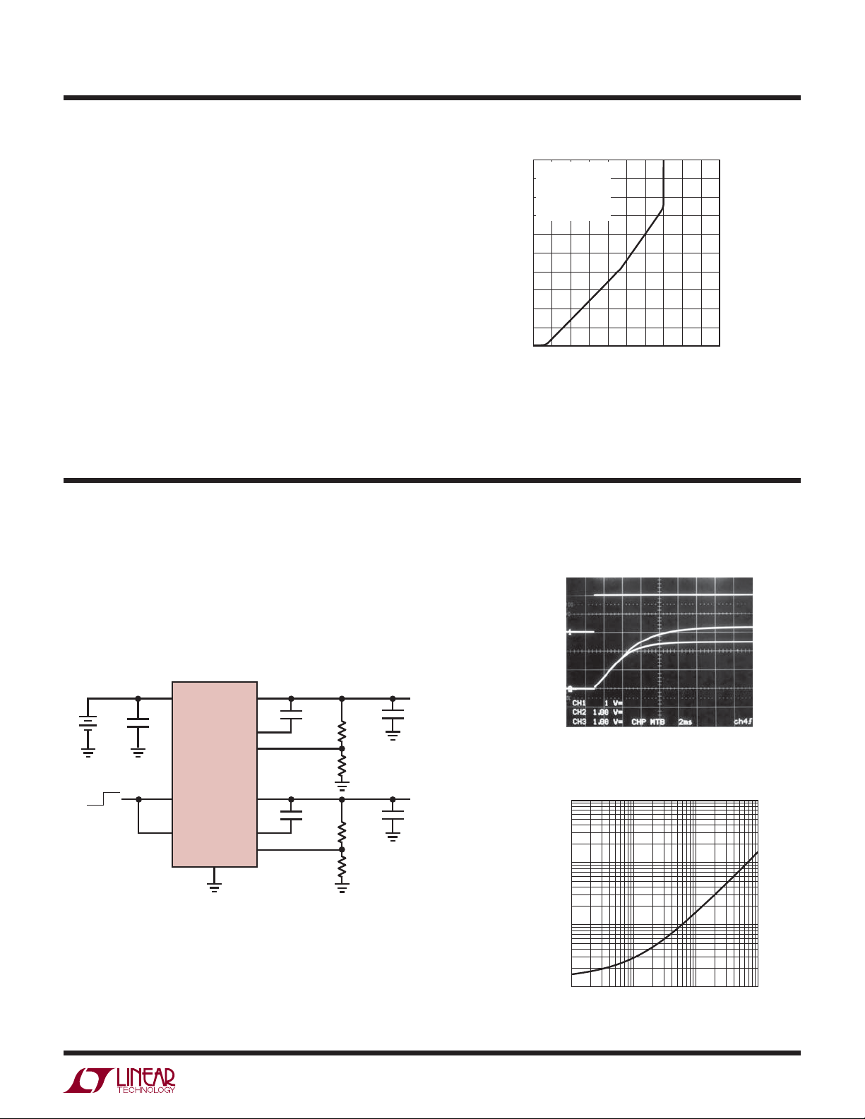
TYPICAL APPLICATIONS
Noise Bypassing Slows Startup, Allows Outputs to Track
100
TA = 25°C
90
= 0V
V
IN
= V
V
OUT
80
760
60
50
40
30
20
REVERSE OUTPUT CURRENT (μA)
10
0
ADJ
CURRENT FLOWS
INTO OUTPUT PIN
0123
OUTPUT VOLTAGE (V)
4
678910
5
Figure 6. Reverse Output Current
3023 F06
V
IN
3.7V TO 20V
OFF ON
1μF
IN
SHDN1
SHDN2
LT3023
GND
OUT1
BYP1
ADJ1
OUT2
BYP2
ADJ2
0.01μF
0.01μF
422k
249k
261k
249k
10μF
10μF
3.3V
AT 100mA
2.5V
AT 100mA
3023 TA02a
V
SHDN1/SHDN2
1V/DIV
V
1V/DIV
V
1V/DIV
OUT1
OUT2
100
10
1
STARTUP TIME (ms)
0.1
10
2ms/DIV
3023 TA02b
Startup Time
100 1000 10000
C
(pF)
BYP
3023 TA02c
3023fa
13
Page 14

LT3023
PACKAGE DESCRIPTION
0.675 ±0.05
DD Package
10-Lead Plastic DFN (3mm × 3mm)
(Reference LTC DWG # 05-08-1699)
R = 0.115
TYP
0.38 ± 0.10
106
3.50 ±0.05
1.65 ±0.05
(2 SIDES)2.15 ±0.05
PACKAGE
OUTLINE
0.25 ± 0.05
0.50
BSC
2.38 ±0.05
(2 SIDES)
RECOMMENDED SOLDER PAD PITCH AND DIMENSIONS
NOTE:
1. DRAWING TO BE MADE A JEDEC PACKAGE OUTLINE M0-229 VARIATION OF (WEED-2).
CHECK THE LTC WEBSITE DATA SHEET FOR CURRENT STATUS OF VARIATION ASSIGNMENT
2. DRAWING NOT TO SCALE
3. ALL DIMENSIONS ARE IN MILLIMETERS
4. DIMENSIONS OF EXPOSED PAD ON BOTTOM OF PACKAGE DO NOT INCLUDE
MOLD FLASH. MOLD FLASH, IF PRESENT, SHALL NOT EXCEED 0.15mm ON ANY SIDE
5. EXPOSED PAD SHALL BE SOLDER PLATED
6. SHADED AREA IS ONLY A REFERENCE FOR PIN 1 LOCATION ON THE
TOP AND BOTTOM OF PACKAGE
PIN 1
TOP MARK
(SEE NOTE 6)
0.200 REF
3.00 ±0.10
(4 SIDES)
0.75 ±0.05
1.65 ± 0.10
(2 SIDES)
0.00 – 0.05
15
0.25 ± 0.05
0.50 BSC
2.38 ±0.10
(2 SIDES)
BOTTOM VIEW—EXPOSED PAD
(DD) DFN 1103
14
3023fa
Page 15

PACKAGE DESCRIPTION
2.794 ± 0.102
(.110 ± .004)
MSE Package
10-Lead Plastic MSOP, Exposed Die Pad
(Reference LTC DWG # 05-08-1664 Rev B)
BOTTOM VIEW OF
EXPOSED PAD OPTION
0.889 ± 0.127
(.035 ± .005)
LT3023
2.06 ± 0.102
1
(.081 ± .004)
1.83 ± 0.102
(.072 ± .004)
5.23
(.206)
MIN
0.305 ± 0.038
(.0120 ± .0015)
TYP
RECOMMENDED SOLDER PAD LAYOUT
0.254
(.010)
GAUGE PLANE
0.18
(.007)
NOTE:
1. DIMENSIONS IN MILLIMETER/(INCH)
2. DRAWING NOT TO SCALE
3. DIMENSION DOES NOT INCLUDE MOLD FLASH, PROTRUSIONS OR GATE BURRS.
MOLD FLASH, PROTRUSIONS OR GATE BURRS SHALL NOT EXCEED 0.152mm (.006") PER SIDE
4. DIMENSION DOES NOT INCLUDE INTERLEAD FLASH OR PROTRUSIONS.
INTERLEAD FLASH OR PROTRUSIONS SHALL NOT EXCEED 0.152mm (.006") PER SIDE
5. LEAD COPLANARITY (BOTTOM OF LEADS AFTER FORMING) SHALL BE 0.102mm (.004") MAX
DETAIL “A”
DETAIL “A”
2.083 ± 0.102
(.082 ± .004)
0.50
(.0197)
BSC
0° – 6° TYP
0.53 ± 0.152
(.021 ± .006)
3.20 – 3.45
(.126 – .136)
SEATING
PLANE
3.00 ± 0.102
(.118 ± .004)
(NOTE 3)
4.90 ± 0.152
(.193 ± .006)
1.10
(.043)
MAX
0.17 – 0.27
(.007 – .011)
TYP
10
12
0.50
(.0197)
BSC
8910
3
7
6
45
0.497 ± 0.076
(.0196 ± .003)
REF
3.00 ± 0.102
(.118 ± .004)
(NOTE 4)
0.86
(.034)
REF
0.1016 ± 0.0508
(.004 ± .002)
MSOP (MSE) 0307 REV B
Information furnished by Linear Technology Corporation is believed to be accurate and reliable.
However, no responsibility is assumed for its use. Linear Technology Corporation makes no representation that the interconnection of its circuits as described herein will not infringe on existing patent rights.
3023fa
15
Page 16
LT3023
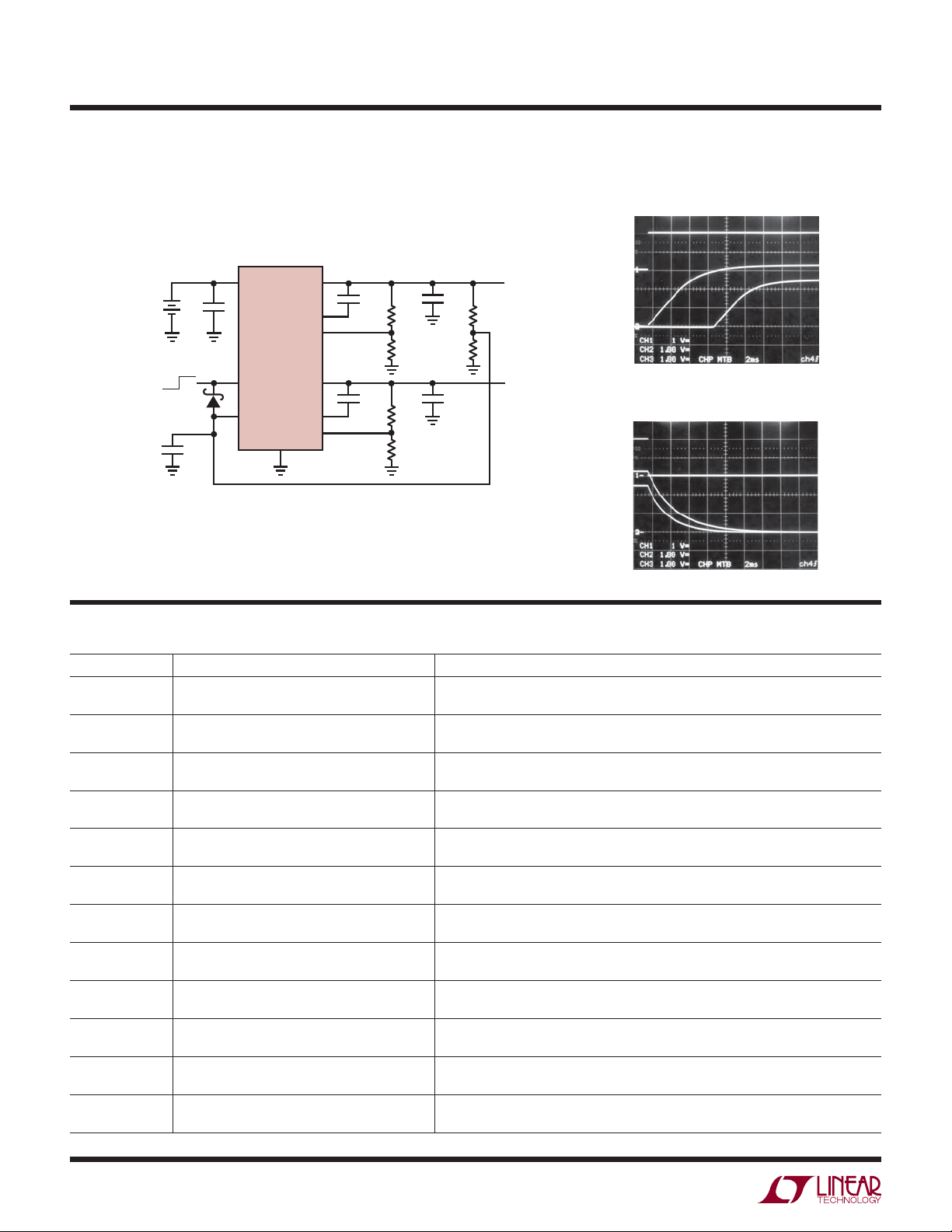
TYPICAL APPLICATION
V
IN
3.7V TO 20V
0.47μF
OFF ON
IN
1μF
SHDN1
SHDN2
LT3023
GND
OUT1
BYP1
ADJ1
OUT2
BYP2
ADJ2
0.01μF
0.01μF
Startup Sequencing
10μF
422k
249k
261k
249k
35.7k
28k
10μF
3.3V
AT
100mA
2.5V
AT
100mA
3023 TA03a
V
SHDN1
1V/DIV
V
OUT1
1V/DIV
V
OUT2
1V/DIV
V
SHDN1
1V/DIV
V
OUT1
1V/DIV
V
OUT2
1V/DIV
Turn-On Waveforms
2ms/DIV
Turn-Off Waveforms
3023 TA03b
2ms/DIV
3023 TA03c
RELATED PARTS
PART NUMBER DESCRIPTION COMMENTS
LT1129 700mA, Micropower, LDO V
: 4.2V to 30V, V
IN
TSSOP20 Packages
LT1175 500mA, Micropower Negative LDO Guaranteed Voltage Tolerance and Line/Load Regulation, VIN: –20V to –4.3V,
V
= –3.8V, IQ = 45μA, ISD = 10μA, DD,SOT-223, S8 Packages
OUT(MIN)
LT1185 3A, Negative LDO Accurate Programmable Current Limit, Remote Sense, V
= –2.40V, I
= 2.5mA, ISD <1μA, TO220-5 Package
Q
LT1761 100mA, Low Noise Micropower, LDO Low Noise < 20μV
V
OUT(MIN) =
1.22V, IQ = 20μA, ISD <1μA, ThinSOT Package
LT1762 150mA, Low Noise Micropower, LDO Low Noise < 20μV
MS8 Package
LT1763 500mA, Low Noise Micropower, LDO Low Noise < 20μV
S8 Package
LT1764/LT1764A 3A, Low Noise, Fast Transient Response, LDO Low Noise < 40μV
V
= 1.21V, IQ = 1mA, ISD <1μA, DD, TO220 Packages
OUT(MIN)
LTC1844 150mA, Very Low Drop-Out LDO Low Noise < 30μV
V
= 1.25V, IQ = 40μA, ISD <1μA, ThinSOT Package
OUT(MIN)
LT1962 300mA, Low Noise Micropower, LDO Low Noise < 20μV
MS8 Package
LT1963/LT1963A 1.5A, Low Noise, Fast Transient Response, LDO Low Noise < 40μV
V
= 1.21V, IQ = 1mA, ISD <1μA, DD, TO220, SOT-223, S8 Packages
OUT(MIN)
LT1964 200mA, Low Noise Micropower, Negative LDO Low Noise < 30μV
LTC3407 Dual 600mA. 1.5MHz Synchronous Step Down
V
V
= –1.21V, IQ = 30μA, ISD = 3μA, ThinSOT Package
OUT(MIN)
: 2.5V to 5.5V, V
IN
DC/DC Converter
Linear Technology Corporation
16
1630 McCarthy Blvd., Milpitas, CA 95035-7417
(408) 432-1900 ● FAX: (408) 434-0507
●
www.linear.com
= 3.75V, IQ = 50μA, ISD = 16μA, DD, SOT-223, S8,TO220,
OUT(MIN)
: –35V to –4.2V, V
IN
Stable with 1μF Ceramic Capacitors, VIN: 1.8V to 20V,
RMS,
: 1.8V to 20V, V
RMS, VIN
: 1.8V to 20V, V
RMS, VIN
"A" Version Stable with Ceramic Capacitors, VIN: 2.7V to 20V,
RMS,
, Stable with 1μF Ceramic Capacitors, VIN: 1.6V to 6.5V,
RMS
: 1.8V to 20V, V
RMS, VIN
"A" Version Stable with Ceramic Capacitors, VIN: 2.1V to 20V,
RMS,
Stable with Ceramic Capacitors, VIN: –0.9V to –20V,
RMS,
= 0.6 V, IQ = 40μA, ISD <1μA, MSE Package
OUT(MIN)
= 1.22V, IQ = 25μA, ISD <1μA,
OUT(MIN)
= 1.22V, IQ = 30μA, ISD <1μA,
OUT(MIN)
= 1.22V, IQ = 30μA, ISD <1μA,
OUT(MIN)
LT 0208 REV A • PRINTED IN USA
© LINEAR TECHNOLOGY CORPORATION 2003
OUT(MIN)
3023fa
 Loading...