

FEATURES
LT1976/LT1976B
High Voltage 1.5A, 200kHz
Step-Down Switching Regulator
with 100μA Quiescent Current
U
DESCRIPTIO
■
Wide Input Range: 3.3V to 60V
■
1.5A Peak Switch Current (LT1976)
■
100μA Quiescent Current (LT1976)**
■
1.6mA Quiescent Current (LT1976B)
■
Low Shutdown Current: IQ < 1μA
■
Power Good Flag with Programmable Threshold
■
Load Dump Protection to 60V
■
200kHz Switching Frequency
■
Saturating Switch Design: 0.2Ω On-Resistance
■
Peak Switch Current Maintained Over
Full Duty Cycle Range*
■
1.25V Feedback Reference Voltage
■
Easily Synchronizable
■
Soft-Start Capability
■
Small 16-Pin Thermally Enhanced TSSOP Package
U
APPLICATIO S
■
High Voltage Power Conversion
■
14V and 42V Automotive Systems
■
Industrial Power Systems
■
Distributed Power Systems
■
Battery-Powered Systems
, LT, LTC and LTM are registered trademarks of Linear Technology Corporation.
Burst Mode is a registered trademark of Linear Technology Corporation.
All other trademarks are the property of their respective owners.
*Protected by U.S. Patents, including 6498466
**See Burst Mode Operation section for conditions
The LT®1976/LT1976B are 200kHz monolithic step-down
switching regulators that accept input voltages up to 60V.
A high efficiency 1.5A, 0.2Ω switch is included on the die
along with all the necessary oscillator, control and logic
circuitry. Current mode topology is used for fast transient
response and good loop stability.
Innovative design techniques along with a new high voltage process achieve high efficiency over a wide input
range. Efficiency is maintained over a wide output current
range by employing Burst Mode operation at low currents,
utilizing the output to bias the internal circuitry, and by
using a supply boost capacitor to fully saturate the power
switch. The LT1976B does not shift into Burst Mode
operation at low currents, eliminating low frequency output ripple at the expense of efficiency. Patented circuitry
maintains peak switch current over the full duty cycle
range.* Shutdown reduces input supply current to less
than 1μA. External synchronization can be implemented
by driving the SYNC pin with logic-level inputs. A single
capacitor from the C
pin to the output provides a
SS
controlled output voltage ramp (soft-start). The devices
also have a power good flag with a programmable threshold and time-out and thermal shutdown protection.
The LT1976/LT1976B are available in a 16-pin TSSOP
package with Exposed Pad leadframe for low thermal
resistance.
TYPICAL APPLICATIO
14V to 3.3V Step-Down Converter with
100μA No Load Quiescent Current
V
3.3V TO 60V
1500pF
10k
IN
1μF
4.7μF
100V
CER
330pF
V
IN
SHDN
V
C
C
T
SYNC
GND
LT1976
BOOST
C
V
BIAS
PGFB
0.33μF
SW
0.1μF
SS
47pF
FB
PG
33μH
10MQ60N
U
4148
165k
1%
100k
1%
V
3.3V
1A
100μF
6.3V
TANT
1976 TA01
OUT
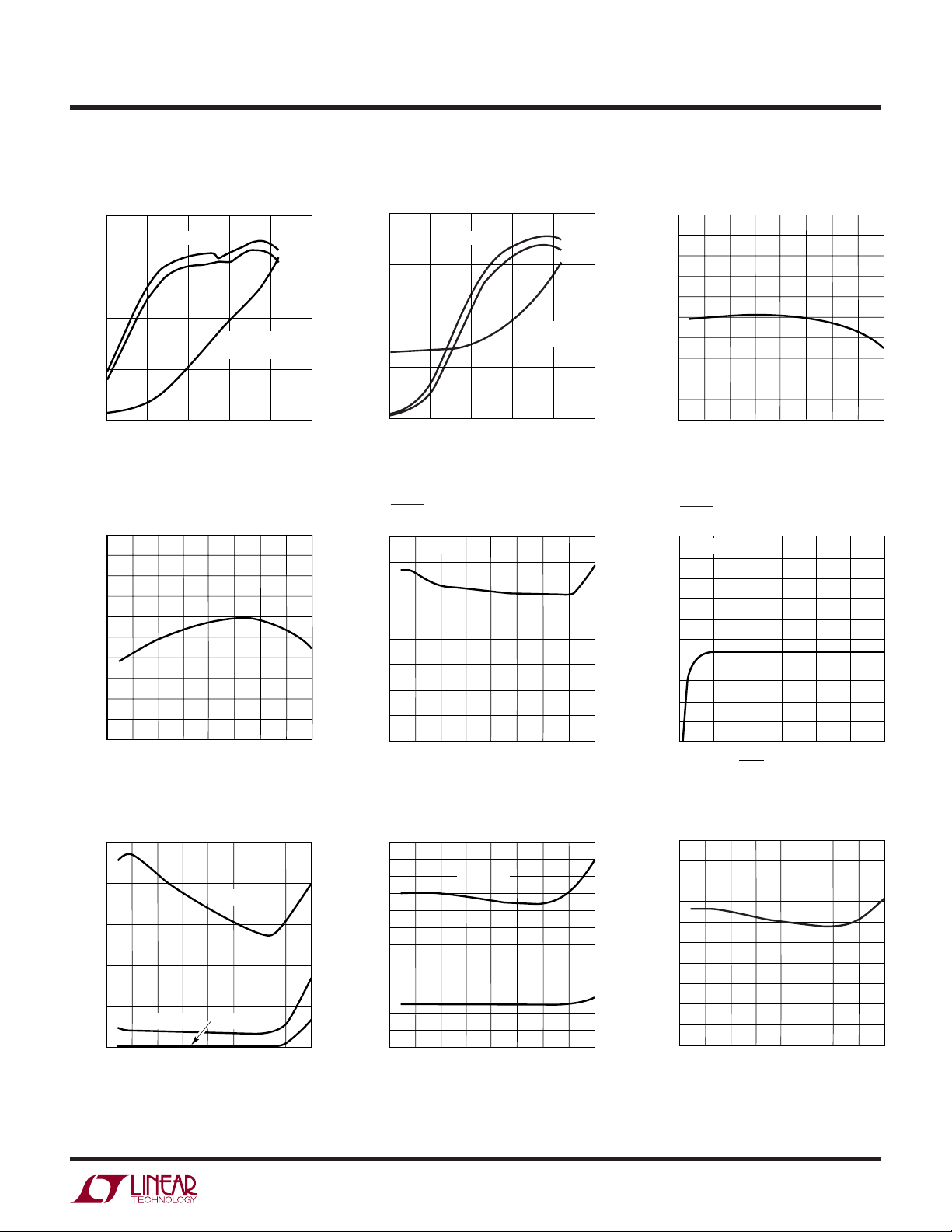
LT1976 Supply Current vs
Input Voltage
150
125
100
75
50
SUPPLY CURRENT (μA)
25
0
0
10
30 40
20
INPUT VOLTAGE (V)
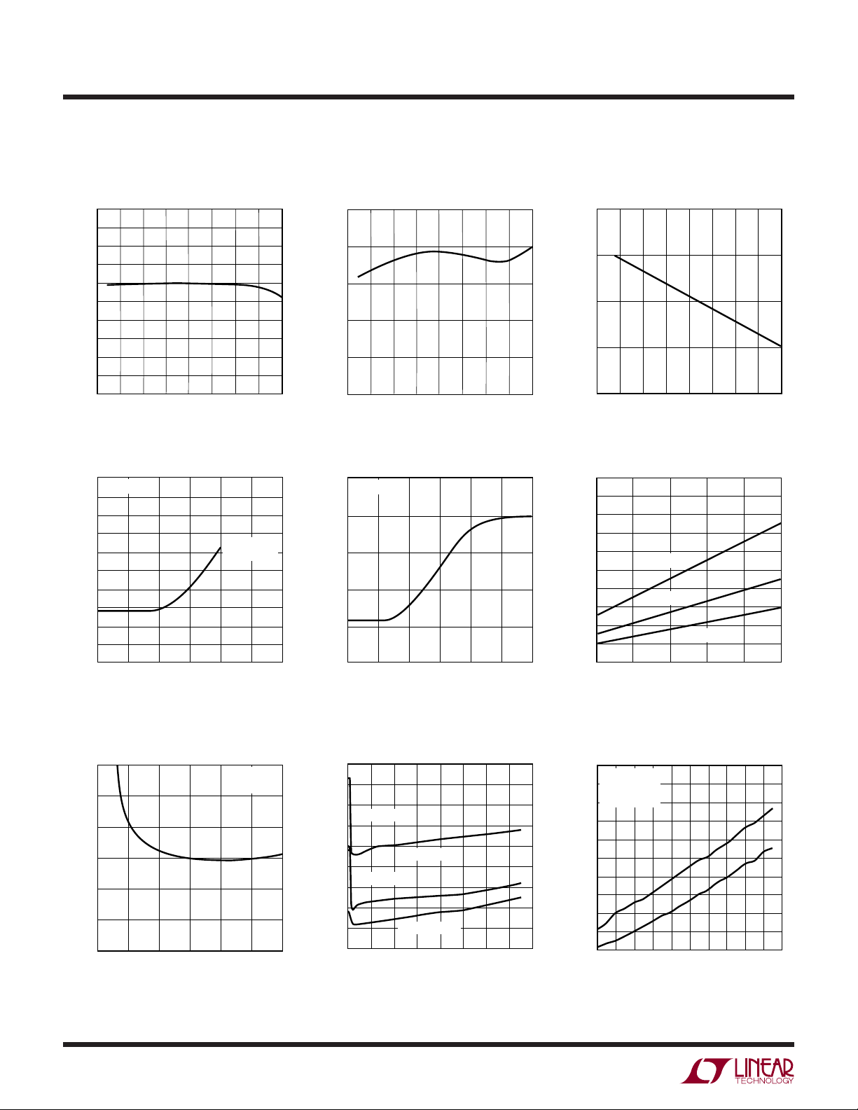
LT1976 Efficiency and Power
Loss vs Load Current
V
= 3.3V
OUT
= 25°C
T
A
50
60
1976 F05
100
75
5V
50
EFFICIENCY (%)
25
0
0.1
EFFICIENCY
3.3V
1
10
LOAD CURRENT (mA)
TYPICAL
POWER LOSS
100
1000
1976 TA02
10000
1976bfg
10
1
POWER LOSS (W)
0.1
0.01
0.001
1
LT1976/LT1976B
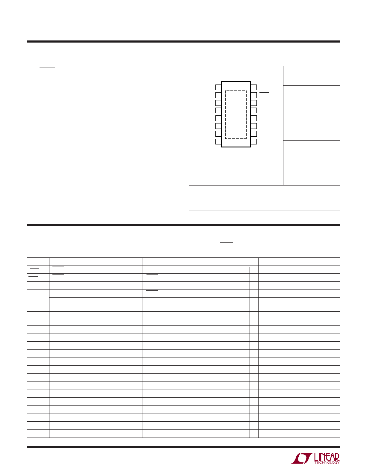
FE PACKAGE
16-LEAD PLASTIC TSSOP
1
2
3
4
5
6
7
8
TOP VIEW
16
15
14
13
12
11
10
9
NC
SW
NC
V
IN
NC
BOOST
C
T
GND
PG
SHDN
SYNC
PGFB
FB
V
C
BIAS
C
SS
17
WW
W
U
ABSOLUTE AXI U RATI GS
(Note 1)
VIN, SHDN, PG, BIAS .............................................. 60V
BOOST Pin Above SW ............................................ 35V
BOOST Pin Voltage ................................................. 68V
SYNC, CSS, PGFB, FB................................................ 6V
Operating JunctionTemperature Range
LT1976EFE/LT1976BEFE (Note 2) ... – 40°C to 125°C
LT1976IFE/LT1976BIFE (Note 2) ..... –40°C to 125°C
LT1976HFE (Note 2) ........................ –40°C to 140°C
Storage Temperature Range ................. –65°C to 150°C
Lead Temperature (Soldering, 10 sec).................. 300°C
UUW
PACKAGE/ORDER I FOR ATIO
ORDER PART
NUMBER
LT1976EFE
LT1976IFE
LT1976HFE
LT1976BEFE
LT1976BIFE
FE PART MARKING
1976EFE
1976IFE
θJA = 45°C/W, θ
EXPOSED PAD IS GND (PIN 17)
MUST BE SOLDERED TO GND (PIN 8)
Order Options Tape and Reel: Add #TR
Lead Free: Add #PBF Lead Free Tape and Reel: Add #TRPBF
Lead Free Part Marking: http://www.linear.com/leadfree/
Consult LTC Marketing for parts specified with wider operating temperature ranges.
JC(PAD)
= 10°C/W
1976HFE
1976BEFE
1976BIFE
ELECTRICAL CHARACTERISTICS
The ● denotes the specifications which apply over the full –40°C to 125°C
operating temperature range, otherwise specifications are at TJ = 25°C. VIN = 12V, SHDN = 12V, BOOST = 15.3V, BIAS = 5V,
FB/PGFB = 1.25V, CSS/SYNC = 0V unless otherwise noted.
SYMBOL PARAMETER CONDITIONS MIN TYP MAX UNITS
V
SHDN
I
SHDN
I
VINS
I
VIN
I
BIASS
I
BIAS
V
REF
I
FB
2
SHDN Threshold ● 1.2 1.3 1.4 V
SHDN Input Current SHDN = 12V ● 520 μA
Minimum Input Voltage (Note 3) ● 2.4 3 V
Supply Shutdown Current SHDN = 0V, BOOST = 0V, FB/PGFB = 0V 0.1 2 μA
Supply Sleep Current (Note 4) (LT1976) BIAS = 0V, FB = 1.35V ● 170 230 μA
Supply Quiescent Current BIAS = 0V, FB = 1.15V, VC = 0.8V (VC = 0V LT1976B) 3.2 4.10 mA
Minimum BIAS Voltage (Note 5) ● 2.7 3 V
BIAS Sleep Current (Note 4) (LT1976) ● 110 180 μA
BIAS Quiescent Current SYNC = 3.3V 700 800 μA
Minimum Boost Voltage (Note 6) ISW = 1.5A 1.8 2.5 V
Input Boost Current (Note 7) ISW = 1.5A 40 50 mA
Reference Voltage (V
FB Input Bias Current 75 200 nA
EA Voltage Gain (Note 8) 900 V/V
EA Voltage g
EA Source Current FB = 1.15V 20 40 55 μA
EA Sink Current FB = 1.35V 15 30 40 μA
VC to SW g
VC High Clamp 2.1 2.2 2.4 V
VC Switching Threshold (LT1976B) ● 0.1 0.4 0.8 V
m
m
) 3.3V < V
REF
FB = 1.35V
BIAS = 5V, FB = 1.15V, VC = 0.8V (VC = 0V LT1976B) 2.6 3.25 mA
< 60V ● 1.225 1.25 1.275 V
VIN
dI(VC)= ±10μA 400 650 800 μMho
● 45 75 μA
3A/V
1976bfg
LT1976/LT1976B
ELECTRICAL CHARACTERISTICS
The ● denotes the specifications which apply over the full –40°C to 125°C
operating temperature range, otherwise specifications are at TJ = 25°C. VIN = 12V, SHDN = 12V, BOOST = 15.3V, BIAS = 5V,
FB/PGFB = 1.25V, C
SYMBOL PARAMETER CONDITIONS MIN TYP MAX UNITS
I
PK
I
CSS
I
PGFB
V
I
CT
V
PGFB
CT
SW Current Limit LT1976 ● 1.5 2.4 3.5 A
Switch On Resistance (Note 9) ● 0.2 0.4 Ω
Switching Frequency BOOST = OPEN ● 180 200 230 kHz
Maximum Duty Cycle 90 92 %
Minimum SYNC Amplitude 1.5 2.0 V
SYNC Frequency Range 230 600 kHz
SYNC Input Impedance SYNC = 0.5V 100 kΩ
CSS Current Threshold (Note 10) FB = 0V 7 13 20 μA
PGFB Input Current 25 100 nA
PGFB Voltage Threshold (Note 11) ● 88 90 92 %
CT Source Current (Note 11) ● 2 3.6 5.5 μA
CT Sink Current (Note 11) 1 2 mA
CT Voltage Threshold (Note 11) 1.16 1.2 1.26 V
PG Leakage (Note 11) PG = 12V 0.1 1 μA
PG Sink Current (Note 11) PGFB = 1V, PG = 400mV 120 200 μA
/SYNC = 0V unless otherwise noted.
SS
LT1976B 1.2 2.5 4 A
The ● denotes the specifications which apply over the full –40°C to 140°C operating temperature range, otherwise specifications are
at TJ = 25°C. VIN = 12V, SHDN = 12V, BOOST = 15.3V, BIAS = 5V, FB/PGFB = 1.25V, CSS/SYNC = 0V unless otherwise noted.
SYMBOL PARAMETER CONDITIONS MIN TYP MAX UNITS
V
SHDN
I
SHDN
I
VINS
I
VIN
I
BIASS
I
BIAS
V
REF
I
FB
SHDN Threshold ● 1.2 1.3 1.4 V
SHDN Input Current SHDN = 12V ● 520 μA
Minimum Input Voltage (Note 3) ● 2.4 3 V
Supply Shutdown Current SHDN = 0V, BOOST = 0V, FB/PGFB = 0V 0.1 2 μA
Supply Sleep Current (Note 4) (LT1976) BIAS = 0V, FB = 1.35V ● 170 300 μA
FB = 1.35V
Supply Quiescent Current BIAS = 0V, FB = 1.15V, VC = 0.8V 3.2 4.10 mA
BIAS = 5V, FB = 1.15V, V
Minimum BIAS Voltage (Note 5) ● 2.7 3 V
BIAS Sleep Current (Note 4) ● 110 180 μA
BIAS Quiescent Current SYNC = 3.3V 700 800 μA
Minimum Boost Voltage (Note 6) ISW = 1.5A 1.8 2.5 V
Input Boost Current (Note 7) ISW = 1.5A 40 50 mA
Reference Voltage (V
FB Input Bias Current 75 200 nA
EA Voltage Gain (Note 8) 900 V/V
EA Voltage g
EA Source Current FB = 1.15V 20 40 55 μA
EA Sink Current FB = 1.35V 15 30 40 μA
VC to SW g
VC High Clamp 2.1 2.2 2.4 V
m
m
) 3.3V < V
REF
dI(VC)= ±10μA 400 650 800 μMho
< 60V ● 1.212 1.25 1.288 V
VIN
= 0.8V 2.6 3.25 mA
C
● 45 100 μA
3A/V
1976bfg
3
LT1976/LT1976B
ELECTRICAL CHARACTERISTICS
The ● denotes the specifications which apply over the full –40°C to 140°C
operating temperature range, otherwise specifications are at TJ = 25°C. VIN = 12V, SHDN = 12V, BOOST = 15.3V, BIAS = 5V,
FB/PGFB = 1.25V, C
SYMBOL PARAMETER CONDITIONS MIN TYP MAX UNITS
I
PK
I
CSS
I
PGFB
V
PGFB
I
CT
V
CT
Note 1: Stresses beyond those listed under Absolute Maximum Ratings
may cause permanent damage to the device. Exposure to any Absolute
Maximum Rating condition for extended periods may affect device
reliability and lifetime.
Note 2: The LT1976EFE/LT1976BEFE are guaranteed to meet performance
specifications from 0°C to 125°C junction temperature. Specifications over
the –40°C to 125°C operating junction temperature range are assured by
design, characterization and correlation with statistical process controls.
The LT1976IFE/LT1976BIFE/LT1976HFE are guaranteed and tested over
the full –40°C to 125°C operating junction temperature range. The
LT1976HFE is also tested to the LT1976HFE electrical characteristics table
at 140°C operating junction temperature. High junction temperatures
degrade operating lifetimes.
Note 3: Minimum input voltage is defined as the voltage where switching
starts. Actual minimum input voltage to maintain a regulated output will
depend upon output voltage and load current. See Applications
Information.
Note 4: Supply input current is the quiescent current drawn by the input
pin. Its typical value depends on the voltage on the BIAS pin and operating
state of the LT1976. With the BIAS pin at 0V, all of the quiescent current
required to operate the LT1976 will be provided by the V
BIAS voltage above its minimum input voltage, a portion of the total
quiescent current will be supplied by the BIAS pin. Supply sleep current
for the LT1976 is defined as the quiescent current during the “sleep”
portion of Burst Mode operation. See Applications Information for
determining application supply currents.
SW Current Limit 2.4 A
Switch On Resistance (Note 9) ● 0.2 0.6 Ω
Switching Frequency BOOST = OPEN ● 150 200 260 kHz
Maximum Duty Cycle 90 92 %
Minimum SYNC Amplitude 1.5 2.0 V
SYNC Frequency Range 230 600 kHz
SYNC Input Impedance SYNC = 0.5V 85 kΩ
CSS Current Threshold (Note 10) 7 13 20 μA
PGFB Input Current 25 100 nA
PGFB Voltage Threshold (Note 11) ● 87 90 93 %
CT Source Current (Note 11) ● 1.5 3.6 5.5 μA
CT Sink Current (Note 11) 1 2 mA
CT Voltage Threshold (Note 11) 1.16 1.2 1.26 V
PG Leakage (Note 11) PG = 12V 0.1 1 μA
PG Sink Current (Note 11) PGFB = 1V, PG = 400mV 120 200 μA
/SYNC = 0V unless otherwise noted.
SS
pin. With the
IN
Note 5: Minimum BIAS voltage is the voltage on the BIAS pin when I
sourced into the pin.
Note 6: This is the minimum voltage across the boost capacitor needed to
guarantee full saturation of the internal power switch.
Note 7: Boost current is the current flowing into the BOOST pin with the
pin held 3.3V above input voltage. It flows only during switch on time.
Note 8: Gain is measured with a V
Note 9: Switch on resistance is calculated by dividing VIN to SW voltage by
the forced current (1.5A LT1976, 1.2A LT1976B). See Typical Performance
Characteristics for the graph of switch voltage at other currents.
Note 10: The C
the C
pin which results in an increase in sink current from the VC pin.
SS
See the Soft-Start section in Applications Information.
Note 11: The PGFB threshold is defined as the percentage of V
which causes the current source output of the C
sinking (below threshold) to sourcing current (above threshold). When
sourcing current, the voltage on the CT pin rises until it is clamped
internally. When the clamp is activated, the output of the PG pin will be set
to a high impedance state. When the C
be set active low with a current sink capability of 200μA.
threshold is defined as the value of current sourced into
SS
swing from 1.15V to 750mV.
C
pin to change from
T
clamp is inactive the PG pin will
T
REF
BIAS
voltage
is
4
1976bfg
UW
1.20
VOLTAGE (V)
1.21
1.23
1.24
1.25
1.30
1.27
1.22
1.28
1.29
1.26
TEMPERATURE (°C)
–50 0
50
75
1976 G01
–25
25
100
150125
TYPICAL PERFOR A CE CHARACTERISTICS
LT1976/LT1976B
LT1976 Efficiency and Power Loss
vs Load Current
100
EFFICIENCY
75
5V
3.3V
50
10
TYPICAL
POWER LOSS
100
EFFICIENCY (%)
25
0
0.1
1
LOAD CURRENT (mA)
1000
10000
1976 TA02
10
1
0.1
0.01
0.001
LT1976B Efficiency and Power
Loss vs Load Current
100
75
POWER LOSS (W)
50
EFFICIENCY (%)
25
0
0.1
1
Oscillator Frequency SHDN Threshold
250
240
230
220
210
200
190
FREQUENCY (kHz)
180
170
160
150
–50
–25
50
25
0
TEMPERATURE (°C)
75
100
150125
1976 G02
1.40
1.35
1.30
1.25
1.20
VOLTAGE (V)
0.15
1.10
1.05
1.00
–50 0 50 75–25 25 100 150125
LT1976 Sleep Mode Supply
Shutdown Supply Current
25
20
15
10
CURRENT (μA)
5
0
–50 0
VIN = 42V VIN = 12V
–25
TEMPERATURE (°C)
25
50
VIN = 60V
75
100
150125
1976 G05
Current
240
220
200
180
160
140
120
100
CURRENT (μA)
80
60
40
20
0
–50 0
–25
EFFICIENCY
5V
3.3V
TYPICAL
POWER LOSS
100
10
LOAD CURRENT (mA)
TEMPERATURE (°C)
V
= 0V
BIAS
V
= 5V
BIAS
50
25
TEMPERATURE (°C)
75
100
1000
10000
1976 G25
1976 G03
1976 G06
10
1
0.1
0.01
0.001
150125
FB Voltage
POWER LOSS (W)
SHDN Pin Current
5.5
TJ = 25°C
5.0
4.5
4.0
3.5
3.0
2.5
CURRENT (μA)
2.0
1.5
1.0
0
0
LT1976 Bias Sleep Current
200
180
160
140
120
100
80
CURRENT (μA)
60
40
20
0
–50 0
10
–25
30 40
20
SHDN VOLTAGE (V)
50
25
TEMPERATURE (°C)
75
100
50
1976 G04
1976 G07
1976bfg
5
60
150125
LT1976/LT1976B
LOAD CURRENT (A)
0
VOLTAGE (mV)
50
150
200
250
500
350
0.7
0.9
1976 G13
100
400
450
300
0.5
1.1
1.3
1.5
TJ = 125°C
TJ = 25°C
TJ = –50°C
UW
TYPICAL PERFOR A CE CHARACTERISTICS
PGFB Threshold
1.20
1.18
1.16
1.14
1.12
1.10
1.08
VOLTAGE (V)
1.06
1.04
1.02
1.00
–50 0
–25
50
25
TEMPERATURE (°C)
Soft-Start Current Threshold
vs FB Voltage
50
TJ = 25°C
45
40
35
30
25
20
CURRENT (μA)
15
10
5
0
0
0.2
0.6 0.8
0.4
FB VOLTAGE (V)
75
100
SOFT-START
DEFEATED
1.0
1976 G08
1976 G11
PG Sink Current
250
200
150
100
CURRENT (μA)
50
150125
0
–50 0
–25
50
25
TEMPERATURE (°C)
75
100
150125
1976 G08
Switch Peak Current Limit
3.5
3.0
2.5
2.0
PEAK SWITCH CURRENT (A)
1.5
–50
–25 –0 25 50
TEMPERATURE (°C)
75 100 150125
1976 G10
Oscillator Frequency
1.2
vs FB Voltage
250
TJ = 25°C
200
150
100
FREQUENCY (kHz)
50
0
0.2
0
0.6 0.8
0.4
FB VOLTAGE (V)
1.0
1.2
1976 G12
Switch On Voltage (V
CESAT
)
LT1976 Supply Current
vs Input Voltage
150
125
100
75
50
SUPPLY CURRENT (μA)
25
0
0
10
6
30 40
20
INPUT VOLTAGE (V)
LT1976 Burst Mode Threshold
Minimum Input Voltage
V
= 3.3V
OUT
= 25°C
T
A
50
60
1976 F05
7.5
7.0
6.5
5V START
6.0
5.5
5.0
3.3V START
4.5
INPUT VOLTAGE (V)
4.0
3.5
3.0
200
0
400
5V RUNNING
3.3V RUNNING
800
600
LOAD CURRENT (mA)
1000
1200
1400
1976 G19
1600
vs Input Voltage
200
V
= 3.3V
OUT
180
L = 33μH
= 100μF
C
OUT
160
140
120
100
80
60
LOAD CURRENT (mA)
40
20
0
97
5
17 19 23
1311
15
INPUT VOLTAGE (V)
21
25
1975 G20
1976bfg
UW
TYPICAL PERFOR A CE CHARACTERISTICS
LT1976B VC Switching Threshold
vs Temperature
700
600
500
400
300
VOLTAGE (V)
C
V
200
100
0
–50
–10 3010–30 50
TEMPERATURE (˚C)
70 90 110
1976 G26
Minimum On Time Boost Current vs Load Current
500
450
400
350
300
LOAD CURRENT = 0.5A
250
200
ON TIME (ns)
150
100
50
0
–50
–30 10
LOAD CURRENT = 1A
–10
30
TEMPERATURE (°C)
50
90
70
110
1976 G21
LT1976/LT1976B
50
45
40
35
30
25
20
15
BOOST CURRENT (mA)
10
5
0
200 600
0
400
LOAD CURRENT (mA)
800
1000
1200
1400
1976 G22
Dropout Operation
4.0
V
= 3.3V
OUT
BOOST DIODE = DIODES INC. B1100
3.5
3.0
2.5
2.0
1.5
OUTPUT VOLTAGE (V)
1.0
0.5
0
2
LOAD CURRENT = 1.25A
LOAD CURRENT = 250mA
2.5 3 4
INPUT VOLTAGE (V)
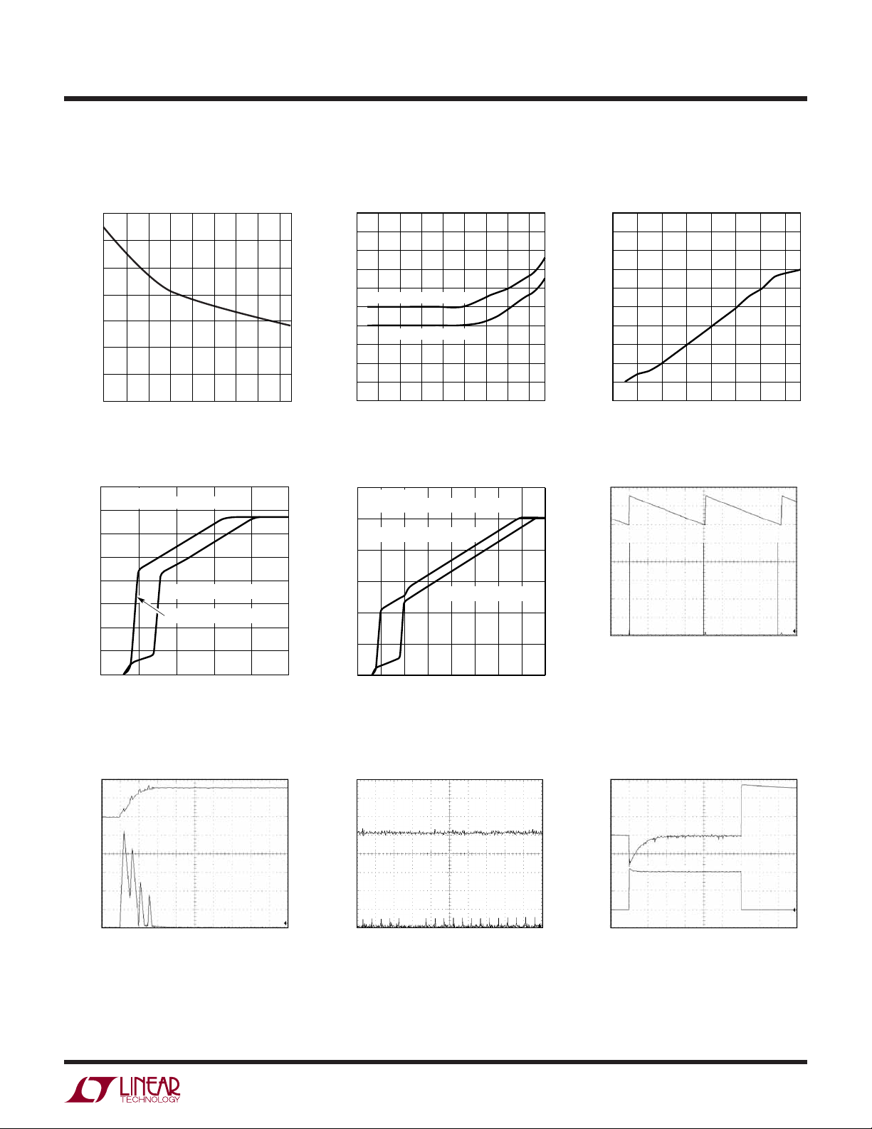
LT1976 Burst Mode Operation
V
OUT
50mV/
DIV
I
SW
100mA/
DIV
0A
= 12V TIME (10μs/DIV) 1976 G15
V
IN
V
= 3.3V
OUT
= 100μA
I
Q
3.5
1976 G23
4.5
Dropout Operation
6
V
BOOST DIODE = DIODES INC. B1100
5
4
3
2
OUTPUT VOLTAGE (V)
1
0
2
LT1976B No Load Operation
(Pulse-Skipping Mode)
V
OUT
50mV/DIV
AC
COUPLED
I
SW
100mA/DIV
0A
V
IN
V
OUT
I
Q
= 5V
OUT
LOAD CURRENT = 250mA
LOAD CURRENT = 1.25A
5
34
2.5 3.5
INPUT VOLTAGE (V)
= 12V TIME (10μs/DIV) 1976 G27
= 3.3V
= 1.6mA
4.5
5.5
1976 G24
100mA/DIV
6
100mV/DIV
500mA/DIV
LT1976 Burst Mode Operation
V
OUT
50mV/DIV
I
SW
0A
= 12V TIME (5ms/DIV) 1976 G14
V
IN
V
= 3.3V
OUT
= 100μA
I
Q
LT1976 No Load 1A
Step Response
V
OUT
1A
I
OUT
0A
= 12V TIME (1ms/DIV) 1976 G17
V
IN
V
= 3.3V
OUT
= 47μF
C
OUT
1976bfg
7
LT1976/LT1976B
UW
TYPICAL PERFOR A CE CHARACTERISTICS
LT1976 Step Response
V
OUT
100mV/DIV
1A
I
OUT
500mA/DIV
0A
= 12V TIME (1ms/DIV) 1976 G18
V
IN
V
= 3.3V
OUT
C
= 47μF
OUT
= 250mA
I
DC
U
UU
PI FU CTIO S
NC (Pins 1, 3, 5): No Connection. Pins 1, 3, 5 are
electrically isolated from the LT1976. They may be connected to PCB traces to aid in PCB layout.
SW (Pin 2): The SW pin is the emitter of the on-chip power
NPN switch. This pin is driven up to the input pin voltage
during switch on time. Inductor current drives the SW pin
negative during switch off time. Negative voltage is clamped
with the external Schottky catch diode to prevent excessive negative voltages.
VIN (Pin 4): This is the collector of the on-chip power NPN
switch. VIN powers the internal control circuitry when a
voltage on the BIAS pin is not present. High di/dt edges
occur on this pin during switch turn on and off. Keep the
path short from the VIN pin through the input bypass
capacitor, through the catch diode back to SW. All trace
inductance on this path will create a voltage spike at switch
off, adding to the VCE voltage across the internal NPN.
BOOST (Pin 6): The BOOST pin is used to provide a drive
voltage, higher than the input voltage, to the internal
bipolar NPN power switch. Without this added voltage, the
typical switch voltage loss would be about 1.5V. The
additional BOOST voltage allows the switch to saturate
and its voltage loss approximates that of a 0.2Ω FET
structure, but with much smaller die area.
CT (Pin 7): A capacitor on the CT pin determines the amount
of delay time between the PGFB pin exceeding its threshold (V
When the PGFB pin rises above V
) and the PG pin set to a high impedance state.
PGFB
, current is sourced
PGFB
from the CT pin into the external capacitor. When the voltage on the external capacitor reaches an internal clamp
(VCT), the PG pin becomes a high impedance node. The
resultant PG delay time is given by t = C
voltage on the PGFB pin drops below V
• VCT/ICT. If the
CT
, CCT will be
PGFB
discharged rapidly to 0V and PG will be active low with a
200μA sink capability. If the CT pin is clamped (Power Good
condition) during normal operation and SHDN is taken low,
the CT pin will be discharged and a delay period will occur
when SHDN is returned high. See the Power Good section
in Applications Information for details.
GND (Pins 8, 17): The GND pin connection acts as the
reference for the regulated output, so load regulation will
suffer if the “ground” end of the load is not at the same
voltage as the GND pin of the IC. This condition will occur
when load current or other currents flow through metal
paths between the GND pin and the load ground. Keep the
path between the GND pin and the load ground short and
use a ground plane when possible. The GND pin also acts
as a heat sink and should be soldered (along with the
exposed leadframe) to the copper ground plane to reduce
thermal resistance (see Applications Information).
8
1976bfg

LT1976/LT1976B
U
UU
PI FU CTIO S
CSS (Pin 9): A capacitor from the CSS pin to the regulated
output voltage determines the output voltage ramp rate
during start-up. When the current through the CSS capacitor exceeds the CSS threshold (I
the output is limited. The C
the FB voltage (see Typical Performance Characteristics)
and is defeated for FB voltage greater than 0.9V (typical).
See Soft-Start section in Applications Information for
details.
BIAS (Pin 10): The BIAS pin is used to improve efficiency
when operating at higher input voltages and light load
current. Connecting this pin to the regulated output voltage forces most of the internal circuitry to draw its
operating current from the output voltage rather than the
input supply. This architecture increases efficiency especially when the input voltage is much higher than the
output. Minimum output voltage setting for this mode of
operation is 3V.
V
(Pin 11): The VC pin is the output of the error amplifier
C
and the input of the peak switch current comparator. It is
normally used for frequency compensation, but can also
serve as a current clamp or control loop override. The V
pin sits about 0.45V for light loads and 2.2V at current
limit. The LT1976 clamps the VC pin slightly below the
burst threshold during sleep periods for better transient
response. Driving the VC pin to ground will disable switching and also place the LT1976 into sleep mode.
FB (Pin 12): The feedback pin is used to determine the
output voltage using an external voltage divider from the
output that generates 1.25V at the FB pin . When the FB pin
drops below 0.9V, switching frequency is reduced, the
SYNC function is disabled and output ramp rate control is
enabled via the CSS pin. See the Feedback section in
Applications Information for details.
SS
), the voltage ramp of
CSS
threshold is proportional to
C
PGFB (PIN 13): The PGFB pin is the positive input to a
comparator whose negative input is set at V
PGFB is taken above V
the C
pin starting the PG delay period. When the voltage
T
on the PGFB pin drops below V
discharged resetting the PG delay period. The PGFB voltage is typically generated by a resistive divider from the
regulated output or input supply. See Power Good section
in Applications Information for details.
SYNC (Pin 14): The SYNC pin is used to synchronize the
internal oscillator to an external signal. It is directly logic
compatible and can be driven with any signal between
20% and 80% duty cycle. The synchronizing range is
equal to maximum initial operating frequency up to 700kHz.
When the voltage on the FB pin is below 0.9V the SYNC
function is disabled. See the Synchronizing section in
Applications Information for details.
SHDN (Pin 15): The SHDN pin is used to turn off the
regulator and to reduce input current to less than 1μA. The
SHDN pin requires a voltage above 1.3V with a typical
source current of 5μA to take the IC out of the shutdown
state.
PG (Pin 16): The PG pin is functional only when the SHDN
pin is above its threshold, and is active low when the
internal clamp on the C
high impedance when the clamp is active. The PG pin has
a typical sink capability of 200μA. See the Power Good
section in Applications Information for details.
, current (I
PGFB
PGFB
pin is below its clamp level and
T
) is sourced into
CSS
, the CT pin is rapidly
PGFB
. When
1976bfg
9

LT1976/LT1976B
BLOCK DIAGRA
V
IN
4
BIAS
10
SYNC
14
SHDN
15
+
SHDN
COMP
–
1.3V
C
SS
9
UNDERVOLTAGE
W
INTERNAL REF
LOCKOUT
THERMAL
SHUTDOWN
SOFT-START
2.4V
SLOPE
COMP
200kHz
OSCILLATOR
ANTISLOPE
COMP
BURST MODE
DETECT
LT1976 ONLY
Σ
CURRENT
COMP
R
S
+
–
SWITCH
LATCH
Q
DRIVER
CIRCUITRY
BOOST
SW
6
2
FOLDBACK
DETECT
FB
12
1.25V
V
C
11
PGFB
13
1.12V
C
T
7
–
ERROR
AMP
+
+
PG
COMP
–
V
C
CLAMP
1.2V C
CLAMP
Figure 1. LT1976/LT1976B Block Diagram
The LT1976 is a constant frequency, current mode buck
converter. This means that there is an internal clock and two
feedback loops that control the duty cycle of the power
switch. In addition to the normal error amplifier, there is a
current sense amplifier that monitors switch current on a
cycle-by-cycle basis. A switch cycle starts with an oscillator pulse which sets the RS latch to turn the switch on. When
switch current reaches a level set by the current comparator the latch is reset and the switch turns off. Output voltage control is obtained by using the output of the error
amplifier to set the switch current trip point. This technique
means that the error amplifier commands current to be
PG
16
T
GND
17
PGND
8
1976 BD
delivered to the output rather than voltage. A voltage fed
system will have low phase shift up to the resonant frequency of the inductor and output capacitor, then an abrupt
180° shift will occur. The current fed system will have 90°
phase shift at a much lower frequency, but will not have the
additional 90° shift until well beyond the LC resonant frequency. This makes it much easier to frequency compensate the feedback loop and also gives much quicker transient response.
Most of the circuitry of the LT1976 operates from an
internal 2.4V bias line. The bias regulator normally draws
10
1976bfg

BLOCK DIAGRA
LT1976/LT1976B
W
power from the VIN pin, but if the BIAS pin is connected to
an external voltage higher than 3V bias power will be
drawn from the external source (typically the regulated
output voltage). This improves efficiency.
High switch efficiency is attained by using the BOOST pin
to provide a voltage to the switch driver which is higher
than the input voltage, allowing switch to be saturated.
This boosted voltage is generated with an external capacitor and diode.
To further optimize efficiency, the LT1976 automatically
switches to Burst Mode operation in light load situations.
WUUU
APPLICATIO S I FOR ATIO
CHOOSING THE LT1976 OR LT1977
The LT1976/LT1976B and LT1977 are high voltage 1.5A
step-down switching regulators. The LT1976 and LT1977
contain circuitry which shifts into burst mode at light loads
reducing quiescent current to typically 100μA. The LT1976B
pulse skips in light load situations, eliminating low frequency burst mode output ripple at the expense of light
load efficiency. The difference between the LT1976/
LT1976B and LT1977 is that the fixed switching frequency
of the LT1976/LT1976B is 200kHz versus 500kHz for the
LT1977. The switching frequency affects: inductor size,
input voltage range in continuous mode operation, efficiency, thermal loss and EMI.
In Burst Mode operation, all circuitry associated with
controlling the output switch is shut down reducing the
input supply current to 45μA.
The only difference between the LT1976 and the LT1976B
is that the LT1976B does not shift into burst mode in light
load situations, eliminating low frequency output ripple at
the expense of light load efficiency.
The LT1976 contains a power good flag with a programmable threshold and delay time. A logic-level low on the
SHDN pin disables the IC and reduces input suppy current
to less than 1μA.
INPUT VOLTAGE RANGE
The minimum on and off times for all versions of the ic are
equivalent. This results in a narrower range of continuous
mode operation for the LT1977. Typical minimum and
maximum duty cycles are 6% to 92% for the LT1976/
LT1976B and 15% to 90% for the LT1977. Both parts will
regulate up to an input voltage of 60V but the LT1977 will
transistion into pulse-skipping/Burst Mode operation when
the input voltage is above 30V for a 5V output. At outputs
above 10V the LT1977’s input range will be similar to the
LT1976/LT1976B. Lowering the input voltage below the
maximum duty cycle limitation will cause a dropout in
regulation.
OUTPUT RIPPLE AND INDUCTOR SIZE
Output ripple current is determined by the input to output
voltage ratio, inductor value and switch frequency. Since
the switch frequency of the LT1977 is 2.5 times greater
than that of the LT1976/LT1976B, the inductance used in
the LT1977 application can be 2.5 times lower than the
LT1976/LT1976B while maintaining the same output ripple
current. The lower value used in the LT1977 application
allows the use of a physically smaller inductor.
Table 1. LT1976/LT1976B/LT1977 Comparison
PARAMETER ADVANTAGE
Minimum Duty Cycle LT1976/LT1976B
Maximum Duty Cycle LT1976/LT1976B
Inductor Size LT1977
Output Capacitor Size LT1977
Efficiency LT1976
EMI LT1976B
Input Range LT1976/LT1976B
Output Ripple LT1977
Light Load Output Ripple LT1976B
1976bfg
11

LT1976/LT1976B
WUUU
APPLICATIO S I FOR ATIO
FEEDBACK PIN FUNCTIONS
The feedback (FB) pin on the LT1976 is used to set output
voltage and provide several overload protection features.
The first part of this section deals with selecting resistors
to set output voltage and the remaining part talks about
frequency foldback and soft-start features. Please read
both parts before committing to a final design.
Referring to Figure 2, the output voltage is determined by
a voltage divider from V
to ground which generates
OUT
1.25V at the FB pin. Since the output divider is a load on the
output care must be taken when choosing the resistor
divider values. For light load applications the resistor
values should be as large as possible to achieve peak
efficiency in Burst Mode operation. Extremely large values
for resistor R1 will cause an output voltage error due to the
50nA FB pin input current. The suggested value for the
output divider resistor (see Figure 2) from FB to ground
(R2) is 100k or less. A formula for R1 is shown below. A
table of standard 1% values is shown in Table 2 for
common output voltages.
RR
12
=+•
V
125 2 50
.•
125
–.
OUT
RnA
For LT1976B aplications, the suggested value for R2 is 10k
or less, eliminating output voltage errors due to feedback
pin current and reducing noise susceptibility.
More Than Just Voltage Feedback
The FB pin is used for more than just output voltage
sensing. It also reduces switching frequency and controls the soft-start voltage ramp rate when output voltage
is below the regulated level (see the Frequency Foldback
and Soft-Start Current graphs in Typical Performance
Characteristics).
Frequency foldback is done to control power dissipation in
both the IC and in the external diode and inductor during
short-circuit conditions. A shorted output requires the
switching regulator to operate at very low duty cycles. As
a result the average current through the diode and inductor is equal to the short-circuit current limit of the switch
(typically 2.4A for the LT1976). Minimum switch on time
limitations would prevent the switcher from attaining a
sufficiently low duty cycle if switching frequency were
maintained at 200kHz, so frequency is reduced by about
4:1 when the FB pin voltage drops below 0.4V (see
Frequency Foldback graph). In addition, if the current in
the switch exceeds 1.5 times the current limitations specified by the V
pin, due to minimum switch on time, the
C
LT1976 will skip the next switch cycle. As the feedback
voltage rises, the switching frequency increases to 200kHz
with 0.95V on the FB pin. During frequency foldback,
external syncronization is disabled to prevent interference
with foldback operation. Frequency foldback does not
affect operation during normal load conditions.
LT1976
OSCILLATOR
12
200kHz
SW
SOFT-START
FOLDBACK
DETECT
ERROR
AMP
Figure 2. Feedback Network
C
–
+
1.25V
V
2
C1
SS
9
FB
12
V
C
11
1976 F02
OUT
R1
R2
In addition to lowering switching frequency the soft-start
ramp rate is also affected by the feedback voltage. Large
Table 2
OUTPUT R1 OUTPUT
VOLTAGE R2 NEAREST (1%) ERROR
(V) (kΩ, 1%) (kΩ)(%)
2.5 100 100 0
3 100 140 0
3.3 100 165 0.38
5 100 300 0
6 100 383 0.63
8 100 536 – 0.63
10 100 698 – 0.25
12 100 866 0.63
1976bfg

WUUU
APPLICATIO S I FOR ATIO
LT1976/LT1976B
capacitive loads or high input voltages can cause a high
input current surge during start-up. The soft-start function reduces input current surge by regulating switch
current via the VC pin to maintain a constant voltage ramp
rate (dV/dt) at the output. A capacitor (C1 in Figure 2) from
the CSS pin to the output determines the maximum output
dV/dt. When the feedback voltage is below 0.4V, the VC pin
will rise, resulting in an increase in switch current and
output voltage. If the dV/dt of the output causes the current
through the CSS capacitor to exceed I
reduced resulting in a constant dV/dt at the output. As the
feedback voltage increases I
increased dV/dt until the soft-start function is defeated
with 0.9V present at the FB pin. The soft-start function
does not affect operation during normal load conditions.
However, if a momentary short (brown out condition) is
present at the output which causes the FB voltage to drop
below 0.9V, the soft-start circuitry will become active.
INPUT CAPACITOR
Step-down regulators draw current from the input supply
in pulses. The rise and fall times of these pulses are very
fast. The input capacitor is required to reduce the voltage
ripple this causes at the input of LT1976 and force the
switching current into a tight local loop, thereby minimizing EMI. The RMS ripple current can be calculated from:
I
I
RIPPLE RMS
Ceramic capacitors are ideal for input bypassing. At 200kHz
switching frequency input capacitor values in the range of
4.7μF to 20μF are suitable for most applications. If opera-
tion is required close to the minimum input required by the
LT1976 a larger value may be required. This is to prevent
excessive ripple causing dips below the minimum operating voltage resulting in erratic operation.
Input voltage transients caused by input voltage steps or
by hot plugging the LT1976 to a pre-powered source such
as a wall adapter can exceed maximum VIN ratings. The
sudden application of input voltage will cause a large
surge of current in the input leads that will store energy in
OUT
V
IN
increases, resulting in an
CSS
VVV
()
OUT IN OUT()
the VC voltage is
CSS
–=
the parasitic inductance of the leads. This energy will
cause the input voltage to swing above the DC level of input
power source and it may exceed the maximum voltage
rating of the input capacitor and LT1976. All input voltage
transient sequences should be observed at the V
the LT1976 to ensure that absolute maximum voltage
ratings are not violated.
The easiest way to suppress input voltage transients is to
add a small aluminum electrolytic capacitor in parallel with
the low ESR input capacitor. The selected capacitor needs
to have the right amount of ESR to critically damp the
resonant circuit formed by the input lead inductance and
the input capacitor. The typical values of ESR will fall in the
range of 0.5Ω to 2Ω and capacitance will fall in the range
of 5μF to 50μF.
If tantalum capacitors are used, values in the 22μF to
470μF range are generally needed to minimize ESR and
meet ripple current and surge ratings. Care should be
taken to ensure the ripple and surge ratings are not
exceeded. The AVX TPS and Kemet T495 series are surge
rated AVX recommends derating capacitor operating voltage by 2:1 for high surge applications.
OUTPUT CAPACITOR
The output capacitor is normally chosen by its effective
series resistance (ESR) because this is what determines
output ripple voltage. To get low ESR takes volume, so
physically smaller capacitors have higher ESR. The ESR
range for typical LT1976 applications is 0.05Ω to 0.2Ω. A
typical output capacitor is an AVX type TPS, 100μF at 10V,
with a guaranteed ESR less than 0.1Ω. This is a “D” size
surface mount solid tantalum capacitor. TPS capacitors
are specially constructed and tested for low ESR, so they
give the lowest ESR for a given volume. The value in
microfarads is not particularly critical and values from
22μF to greater than 500μF work well, but you cannot
cheat Mother Nature on ESR. If you find a tiny 22μF solid
tantalum capacitor, it will have high ESR and output ripple
voltage could be unacceptable. Table 3 shows some
typical solid tantalum surface mount capacitors.
pin of
IN
1976bfg
13

LT1976/LT1976B
I
VVV
VLf
OUT IN OUT
IN
P-P
=
()
()()()
–
WUUU
APPLICATIO S I FOR ATIO
Table 3. Surface Mount Solid Tantalum Capacitor ESR
and Ripple Current
E CASE SIZE ESR MAX (Ω) RIPPLE CURRENT (A)
AVX TPS 0.1 to 0.3 0.7 to 1.1
D CASE SIZE
AVX TPS 0.1 to 0.3 0.7 to 1.1
C CASE SIZE
AVX TPS 0.2 0.5
Many engineers have heard that solid tantalum capacitors
are prone to failure if they undergo high surge currents.
This is historically true and type TPS capacitors are
specially tested for surge capability but surge ruggedness
is not a critical issue with the output capacitor. Solid
tantalum capacitors fail during very high turn-on surges
which do not occur at the output of regulators. High
discharge surges, such as when the regulator output is
dead shorted, do not harm the capacitors.
Unlike the input capacitor RMS, ripple current in the
output capacitor is normally low enough that ripple current rating is not an issue. The current waveform is
triangular with a typical value of 200mA
. The formula
RMS
to calculate this is:
Output capacitor ripple current (RMS)
.–
VVV
029
I
RIPPLE RMS
()
()( )
=
OUT IN OUT
LfV
()()( )
IN
I
P-P
=
12
filter capacitor CF in parallel with the RC/CC network, along
with a small feedforward capacitor C
, is suggested to
FB
control possible ripple at the VC pin. The LT1976 can be
stabilized using a 47μF ceramic output capacitor and V
C
component values of CC = 0.047μF, RC = 12.5k, CF = 100pF
and CFB = 27pF.
OUTPUT RIPPLE VOLTAGE
Figure 3 shows a typical output ripple voltage waveform
for the LT1976. Ripple voltage is determined by the
impedance of the output capacitor and ripple current
through the inductor. Peak-to-peak ripple current through
the inductor into the output capacitor is:
For high frequency switchers the ripple current slew rate
is also relevant and can be calculated from:
didtV
IN
=
L
Peak-to-peak output ripple voltage is the sum of a triwave
created by peak-to-peak ripple current times ESR and a
square wave created by parasitic inductance (ESL) and
ripple current slew rate. Capacitive reactance is assumed
to be small compared to ESR or ESL.
CERAMIC CAPACITORS
Higher value, lower cost ceramic capacitors are now
becoming available. They are generally chosen for their
good high frequency operation, small size and very low
ESR (effective series resistance). Low ESR reduces output
ripple voltage but also removes a useful zero in the loop
frequency response, common to tantalum capacitors. To
compensate for this a resistor RC can be placed in series
with the VC compensation capacitor CC (Figure 10). Care
must be taken however since this resistor sets the high
frequency gain of the error amplifier including the gain at
the switching frequency. If the gain of the error amplifier
is high enough at the switching frequency output ripple
voltage (although smaller for a ceramic output capacitor)
may still affect the proper operation of the regulator. A
14
V I ESR ESL
RIPPLE
47μF TANTALUM
ESR 100mΩ
47μF CERAMIC
=
()( )+()
P-P
V
OUT
20mV/DIV
V
OUT
20mV/DIV
V
SW
5V/DIV
V
= 12V 1μs/DIV 1976 F03
IN
V
= 3.3V
OUT
I
= 1A
LOAD
L = 33μH
Figure 3. LT1976 Ripple Voltage Waveform
di
dt
1976bfg

WUUU
APPLICATIO S I FOR ATIO
LT1976/LT1976B
Example: with V
0.08Ω, ESL = 10nH:
I
=
P-P
di
dt e
V
= 0.0289 + 0.003 = 32mV
MAXIMUM OUTPUT LOAD CURRENT
Maximum load current for a buck converter is limited by
the maximum switch current rating (IPK). The current
rating for the LT1976 is 1.5A. Unlike most current mode
converters, the LT1976 maximum switch current limit
does not fall off at high duty cycles. Most current mode
converters suffer a drop off of peak switch current for duty
cycles above 50%. This is due to the effects of slope
compensation required to prevent subharmonic oscillations in current mode converters. (For detailed analysis,
see Application Note 19.)
The LT1976 is able to maintain peak switch current limit
over the full duty cycle range by using patented circuitry to
cancel the effects of slope compensation on peak switch
current without affecting the frequency compensation it
provides.
12 33 6 200 3
()
12
==
33 5
.–
= (0.362A)(0.08) + (10e – 9)(363e3)
RIPPLE
= 12V, V
IN
33 12 33
.–.
()( )
ee
−
()()
363 5
.
e
= 3.3V, L = 33μH, ESR =
OUT
.
=
0 362
P-P
A
For V
Note that there is less load current available at the higher
input voltage because inductor ripple current increases. At
V
IN
conditions:
To calculate actual peak switch current in continuous
mode with a given set of conditions, use:
If a small inductor is chosen which results in discontinous
mode operation over the entire load range, the maximum
load current is equal to:
= 5V, V
OUT
I
OUT MAX()
= 15V, duty cycle is 33% and for the same set of
I
OUT MAX()
II
SW PK OUT
I
OUT MAX
=+
()
()
= 8V and L = 20μH:
IN
–
58 5
.–
=
15
.–. .
==
15 024 126
.–
=
15
.–. .
==
15 042 108
VVV
IfLV
PK IN
=
2
VVV
()( )
OUT IN OUT
()( )
ee
–
2 20 6 200 3 8
()()()
A
–
515 5
()( )
ee
–
2 20 6 200 3 15
()()()
A
OUT IN OUT
2
2
2
()( )( )
–
()
LfV
()()( )
IN
–
Maximum load current would be equal to maximum
switch current for an infinitely large inductor, but with
finite inductor size, maximum load current is reduced by
one-half peak-to-peak inductor current. The following
formula assumes continuous mode operation, implying
that the term on the right (I
VVV
()( )
II
OUT MAX PK
()
Discontinuous operation occurs when:
VVV
I
OUT DIS
()
OUT IN OUT
≤
OUT IN OUT
–
()
2
()()( )
LfV
/2) is less than I
P-P
–
2
LfV
()()( )
–
IN
IN
.
OUT
I
-P
P
–=
=
I
PK
2
CHOOSING THE INDUCTOR
For most applications the output inductor will fall in the
range of 15μH to 100μH. Lower values are chosen to
reduce physical size of the inductor. Higher values allow
more output current because they reduce peak current
seen by the LT1976 switch, which has a 1.5A limit. Higher
values also reduce output ripple voltage and reduce core
loss.
When choosing an inductor you might have to consider
maximum load current, core and copper losses, allowable component height, output voltage ripple, EMI, fault
current in the inductor, saturation and of course cost.
The following procedure is suggested as a way of handling these somewhat complicated and conflicting
requirements.
1976bfg
15

LT1976/LT1976B
WUUU
APPLICATIO S I FOR ATIO
1. Choose a value in microhenries from the graph of
maximum load current. Choosing a small inductor with
lighter loads may result in discontinuous mode of
operation, but the LT1976 is designed to work well in
either mode.
Table 4. Inductor Selection Criteria
VENDOR/
PART NUMBER VALUE (μH) I
Coiltronics
UP2B-150 15 2.4 0.041 6
UP2B-330 33 1.7 0.062 6
UP2B-470 47 1.4 0.139 6
UP2B-680 68 1.2 0.179 6
UP2B-101 100 0.95 0.271 6
UP3B-150 15 3.9 0.032 6.8
UP3B-330 33 2.4 0.069 6.8
UP3B-470 47 1.9 0.101 6.8
UP3B-680 68 1.6 0.156 6.8
UP3B-101 100 1.4 0.205 6.8
Sumida
CDRH8D28-150M 15 2.2 0.053 3
CDRH124-150M 15 3.2 0.05 4.5
CDRH127-150M 15 4.5 0.02 8
CDRH8D28-330M 33 1.4 0.122 3
CDRH124-330M 33 2.7 0.97 4.5
CDRH127-330M 33 3.0 0.048 8
CDRH8D28-470M 47 1.25 0.150 3
CDRH125-470M 47 1.8 0.058 6
CDRH127-470M 47 2.5 0.076 8
CDRH124-680M 68 1.5 0.228 4.5
CDRH127-680M 68 2.1 0.1 8
CDRH124-101M 100 1.2 0.30 4.5
CDRH127-101M 100 1.7 0.17 8
Coilcraft
DT3308P-153 15 2.0 0.1 3
DT3308P-333 33 1.4 0.3 3
DT3308P-473 47 1 0.47 3
(A) DCR (Ω) HEIGHT (mm)
RMS
Assume that the average inductor current is equal to
load current and decide whether or not the inductor
must withstand continuous fault conditions. If maximum load current is 0.5A, for instance, a 0.5A inductor
may not survive a continuous 2A overload condition.
For applications with a duty cycle above 50%, the
inductor value should be chosen to obtain an inductor
ripple current of less than 40% of the peak switch
current.
2. Calculate peak inductor current at full load current to
ensure that the inductor will not saturate. Peak current
can be significantly higher than output current, especially
with smaller inductors and lighter loads, so don’t omit
this step. Powdered iron cores are forgiving because they
saturate softly, whereas ferrite cores saturate abruptly.
Other core materials fall somewhere in between. The
following formula assumes continuous mode of operation, but it errs only slightly on the high side for discontinuous mode, so it can be used for all conditions.
II
=+
PEAK OUT
VVV
OUT IN OUT
2
–
()
fLV
()( )( )
IN
VIN = maximum input voltage
f = switching frequency, 200kHz
3. Decide if the design can tolerate an “open” core geometry like a rod or barrel, which have high magnetic field
radiation, or whether it needs a closed core like a toroid
to prevent EMI problems. This is a tough decision
because the rods or barrels are temptingly cheap and
small and there are no helpful guidelines to calculate
when the magnetic field radiation will be a problem.
4. After making an initial choice, consider the secondary
things like output voltage ripple, second sourcing, etc.
Use the experts in the Linear Technology’s applications
department if you feel uncertain about the final choice.
They have experience with a wide range of inductor
types and can tell you about the latest developments in
low profile, surface mounting, etc.
16
1976bfg

WUUU
APPLICATIO S I FOR ATIO
LT1976/LT1976B
Short-Circuit Considerations
The LT1976 is a current mode controller. It uses the V
node voltage as an input to a current comparator which
turns off the output switch on a cycle-by-cycle basis as
this peak current is reached. The internal clamp on the V
node, nominally 2.2V, then acts as an output switch peak
current limit. This action becomes the switch current limit
specification. The maximum available output power is
then determined by the switch current limit.
A potential controllability prod}m could occur under shortcircuit conditions. If the power supply output is short
circuited, the feedback amplifier responds to the low
output voltage by raising the control voltage, VC, to its
peak current limit value. Ideally, the output switch would
be turned on, and then turned off as its current exceeded
the value indicated by VC. However, there is finite response
time involved in both the current comparator and turn-off
of the output switch. These result in a minimum on time
t
ON(MIN).
(VF + I • R), the diode forward voltage plus inductor I • R
voltage drop, the potential exists for a loss of control.
Expressed mathematically the requirement to maintain
control is:
where:
If this condition is not observed, the current will not be
limited at IPK but will cycle-by-cycle ratchet up to some
higher value. Using the nominal LT1976 clock frequency
of 200kHz, a VIN of 40V and a (VF + I • R) of say 0.7V, the
maximum tON to maintain control would be approximately
90ns, an unacceptably short time.
When combined with the large ratio of VIN to
VIR
•≤+
ft
•
ON
f = switching frequency
tON = switch on time
VF = diode forward voltage
VIN = Input voltage
I • R = inductor I • R voltage drop
F
V
IN
C
C
The solution to this dilemma is to slow down the oscillator
to allow the current in the inductor to drop to a sufficiently
low value such that the current doesn’t continue to ratchet
higher. When the FB pin voltage is abnormally low thereby
indicating some sort of short-circuit condition, the oscillator frequency will be reduced. Oscillator frequency is
reduced by a factor of 4 when the FB pin voltage is below
0.4V and increases linearly to its typical value of 200kHz at
a FB voltage of 0.95V (see Typical Performance Characteristics). In addition, if the current in the switch exceeds 1.5
current demanded by the VC pin, the LT1976 will skip
• I
PK
the next on cycle effectively reducing the oscillator frequency by a factor of 2. These oscillator frequency reductions during short-circuit conditions allow the LT1976 to
maintain current control.
SOFT-START
For applications where [V
large input surge currents can’t be tolerated, the LT1976
soft-start feature should be used to control the output
capacitor charge rate during start-up, or during recovery
from an output short circuit thereby adding additional
control over peak inductor current. The soft-start function
limits the switch current via the VC pin to maintain a
constant voltage ramp rate (dV/dt) at the output capacitor.
A capacitor (C1 in Figure 2) from the CSS pin to the
regulated output voltage determines the output voltage
ramp rate. When the current through the CSS capacitor
exceeds the CSS threshold (I
output capacitor is limited by reducing the VC pin voltage.
The CSS threshold is proportional to the FB voltage (see
Typical Performance Characteristics) and is defeated for
FB voltages greater than 0.9V (typical). The output dV/dt
can be approximated by:
dVdtI
CSS
=
C
SS
but actual values will vary due to start-up load conditions,
compensation values and output capacitor selection.
IN
/(V
+ VF)] ratios > 10 or
OUT
), the voltage ramp of the
CSS
1976bfg
17

LT1976/LT1976B
WUUU
APPLICATIO S I FOR ATIO
C
= GND
V
0.5V/DIV
SS
OUT
C
= 0.1μFC
SS
C
= 47μF TIME (1ms/DIV) 1976 F04
OUT
I
= 200mA
LOAD
= 12V
V
IN
Figure 4. V
OUT
dV/dt
= 0.1μF
SS
Burst Mode OPERATION (LT1976 ONLY)
To enhance efficiency at light loads, the LT1976 automatically switches to Burst Mode operation which keeps the
output capacitor charged to the proper voltage while minimizing the input quiescent current. During Burst Mode
operation, the LT1976 delivers short bursts of current to
the output capacitor followed by sleep periods where the
output power is delivered to the load by the output capacitor. In addition, VIN and BIAS quiescent currents are reduced to typically 45μA and 125μA respectively during the
sleep time. As the load current decreases towards a no
load condition, the percentage of time that the LT1976
operates in sleep mode increases and the average input
current is greatly reduced resulting in higher efficiency.
The minimum average input current depends on the VIN to
V
ratio, VC frequency compensation, feedback divider
OUT
network and Schottky diode leakage. It can be approximated by the following equation:
Example: For V
45 5
IAA
IN AVG()
=μ+μ+
45 5 47 97
=μ+μ+μ=μ
During the sleep portion of the Burst Mode cycle, the V
= 3.3V, VIN = 12V
OUT
μ+ μ+
125 12 5 0
AA
()
33
.
⎞
⎛
⎟
⎜
⎠
⎝
12
AA A A
.
08
()
...5
μ
A
C
pin voltage is held just below the level needed for normal
operation to improve transient response. See the Typical
Performance Characteristics section for burst and transient response waveforms.
If a no load condition can be anticipated, the supply current
can be further reduced by cycling the SHDN pin at a rate
higher than the natural no load burst frequency. Figure 6
shows Burst Mode operation with the SHDN pin. V
OUT
burst ripple is maintained while the average supply current
150
125
100
75
50
SUPPLY CURRENT (μA)
25
0
10
0
30 40
20
INPUT VOLTAGE (V)
Figure 5. IQ vs V
V
IN
OUT
T
= 3.3V
= 25°C
A
50
60
1976 F05
III
III
IN AVG VINS SHDN
≅+ +
()
⎛
⎜
⎝
V
⎞
()
OUT
⎟
⎠
V
IN
++
BIASS FB S
η
()
where
I
= input pin current in sleep mode
VINS
V
= output voltage
OUT
V
input voltage
IN =
I
= BIAS pin current in sleep mode
BIASS
IFB = feedback network current
IS = catch diode reverse leakage at V
OUT
η = low current efficiency (non Burst Mode operation)
18
V
OUT
50mV/DIV
V
SHDN
2V/DIV
I
SW
500mA/DIV
V
= 12V TIME (50ms/DIV) 1976 G16
IN
V
= 3.3V
OUT
= 15μA
I
Q
Figure 6. Burst Mode with Shutdown Pin
1976bfg
WUUU
APPLICATIO S I FOR ATIO
LT1976/LT1976B
drops to 15μA. The PG pin will be active low during the
“on” portion of the SHDN waveform due to the C
capaci-
T
tor discharge when SHDN is taken low. See the Power
Good section for further information.
CATCH DIODE
The catch diode carries load current during the SW off
time. The average diode current is therefore dependent on
the switch duty cycle. At high input to output voltage ratios
the diode conducts most of the time. As the ratio approaches unity the diode conducts only a small fraction of
the time. The most stressful condition for the diode is
when the output is short circuited. Under this condition the
diode must safely handle I
at maximum duty cycle.
PEAK
To maximize high and low load current efficiency a fast
switching diode with low forward drop and low reverse
leakage should be used. Low reverse leakage is critical to
maximize low current efficiency since its value over temperature can potentially exceed the magnitude of the
LT1976 supply current. Low forward drop is critical for
high current efficiency since the loss is proportional to
forward drop.
These requirements result in the use of a Schottky type
diode. DC switching losses are minimized due to its low
forward voltage drop and AC behavior is benign due to its
lack of a significant reverse recovery time. Schottky diodes
are generally available with reverse voltage ratings of 60V
and even 100V and are price competitive with other types.
Table 5. Catch Diode Selection Criteria
IQ at 125°C EFFICIENCY
LEAKAGE V
V
= 3.3V VF AT 1A V
OUT
DIODE 25°C 125°C25°C 125°CIL = 0A IL = 1A
IR 10BQ100 0.0μA59μA 0.72V 0.58V 125μA 74.1%
Diodes Inc. 0.1μA 242μA 0.48V 0.41V 215μA 82.8%
B260SMA
Diodes Inc. 0.2μA 440μA 0.45V 0.36V 270μA 83.6%
B360SMB
IR 1μA 1.81mA 0.42V 0.34V 821μA 83.7%
MBRS360TR
IR 30BQ100 1.7μA 2.64mA 0.40V 0.32V 1088μA 84.5%
=12V VIN =12V
IN
= 3.3 V
OUT
OUT
= 3.3V
The effect of reverse leakage and forward drop on efficiency for various Schottky diodes is shown in Table 4. As
can be seen these are conflicting parameters and the user
must weigh the importance of each specification in choosing the best diode for the application.
The use of so-called “ultrafast” recovery diodes is generally not recommended. When operating in continuous
mode, the reverse recovery time exhibited by “ultrafast”
diodes will result in a slingshot type effect. The power
internal switch will ramp up VIN current into the diode in an
attempt to get it to recover. Then, when the diode has
finally turned off, some tens of nanoseconds later, the V
SW
node voltage ramps up at an extremely high dV/dt, perhaps 5V to even 10V/ns! With real world lead inductances
the VSW node can easily overshoot the VIN rail. This can
result in poor RFI behavior and, if the overshoot is severe
enough, damage the IC itself.
BOOST PIN
For most applications the boost components are a 0.33μF
capacitor and a MMSD914 diode. The anode is typically
connected to the regulated output voltage to generate a
voltage approximately V
above VIN to drive the output
OUT
stage (Figure 7a). However, the output stage discharges
the boost capacitor during the on time of the switch. The
output driver requires at least 2.5V of headroom throughout this period to keep the switch fully saturated. If the
output voltage is less than 3.3V it is recommended that an
alternate boost supply is used. The boost diode can be
connected to the input (Figure 7b) but care must be taken
to prevent the boost voltage (V
= VIN • 2) from
BOOST
exceeding the BOOST pin absolute maximum rating. The
additional voltage across the switch driver also increases
power loss and reduces efficiency. If available, an independent supply can be used to generate the required
BOOST voltage (Figure 7c). Tying BOOST to VIN or an
independent supply may reduce efficiency but it will reduce the minimum VIN required to start-up with light
loads. If the generated BOOST voltage dissipates too
much power at maximum load, the BOOST voltage the
LT1976 sees can be reduced by placing a Zener diode in
series with the BOOST diode (Figure 7a option).
1976bfg
19
LT1976/LT1976B
WUUU
APPLICATIO S I FOR ATIO
OPTIONAL
BOOST
V
IN
V
IN
V
IN
Figure 7. BOOST Pin Configurations
V
V
BOOST
V
BOOST(MAX)
V
V
BOOST
V
BOOST(MAX)
V
V
BOOST
V
BOOST(MAX)
IN
LT1976
– VSW = V
= VIN + V
BOOST
IN
LT1976
– VSW = V
BOOST
IN
LT1976
– VSW = V
= VDC + V
SWGND
SWGND
= 2V
SWGND
OUT
(7a)
IN
IN
(7b)
DC
(7c)
OUT
D
SS
IN
1976 F07
SHUTDOWN FUNCTION AND UNDERVOLTAGE
LOCKOUT
V
OUT
The SHDN pin on the LT1976 controls the operation of the
IC. When the voltage on the SHDN pin is below the 1.2V
shutdown threshold the LT1976 is placed in a “zero”
supply current state. Driving the SHDN pin above the
shutdown threshold enables normal operation. The SHDN
pin has an internal sink current of 3μA.
In addition to the shutdown feature, the LT1976 has an
undervoltage lockout function. When the input voltage is
below 2.4V, switching will be disabled. The undervoltage
lockout threshold doesn’t have any hysteresis and is
V
OUT
mainly used to insure that all internal voltages are at the
correct level before switching is enabled. If an undervoltage lockout function with hysteresis is needed to limit
input current at low VIN to V
ratios refer to Figure 8 and
OUT
the following:
V
DC
VR
V
OUT
UVLO
V
HYST
V
⎛
=++
=
SHDN SHDN
1
⎜
R
⎝
VR
()
OUT
R
3
V
IV
32
R
SHDN SHDN
1
⎞
+
⎟
⎠
R1 should be chosen to minimize quiescent current during
normal operation by the following equation:
A 0.33μF boost capacitor is recommended for most appli-
cations. Almost any type of film or ceramic capacitor is
suitable but the ESR should be <1Ω to ensure it can be fully
recharged during the off time of the switch. The capacitor
value is derived from worst-case conditions of 4700ns on
time, 42mA boost current and 0.7V discharge ripple. The
boost capacitor value could be reduced under less demanding conditions but this will not improve circuit operation or efficiency. Under low input voltage and low load
conditions a higher value capacitor and Schottky boost
diode will reduce discharge ripple and improve start-up
and dropout operation.
20
R
1
=
Example:
R
1
=
R
=
3
R2 =
=
–
VV
2
IN
.
I
15
()
()
SHDN MAX
()
12 2
–
155
A
.
μ
()
M
513
Ω
.
()
M
=Ω
13
.
M
=Ω Ω
65
.
(Nearest 1% 6.49M )
1
1.3
13
649
.
.
M
Ω
7 – 1.3
Ω
1.3M
k
408
(Nearest 1% 412k)
A
μ
1
––
1976bfg

WUUU
APPLICATIO S I FOR ATIO
LT1976
V
IN
4
R1
R3
V
OUT
SHDN
15
R2
3μA
+
V
IN
COMP
–
2.4V
+
SHDN
COMP
–
1.3V
Figure 8. Undervoltage Lockout
LT1976/LT1976B
ENABLE
1976 F08
See the Typical Performance Characteristics section for
graphs of SHDN and VIN currents verses input voltage.
SYNCHRONIZING
Oscillator synchronization to an external input is achieved
by connecting a TTL logic-compatible square wave with a
duty cycle between 20% and 80% to the LT1976 SYNC
pin. The synchronizing range is equal to initial operating
frequency up to 700kHz. This means that minimum
practical sync frequency is equal to the worst-case high
self-oscillating frequency (230kHz), not the typical operating frequency of 200kHz. Caution should be used when
synchronizing above 230kHz because at higher sync
frequencies the amplitude of the internal slope compensation used to prevent subharmonic switching is reduced. This type of subharmonic switching only occurs at
input voltages less than twice output voltage. Higher
inductor values will tend to eliminate this problem. See
Frequency Compensation section for a discussion of an
entirely different cause of subharmonic switching before
assuming that the cause is insufficient slope compensation. Application Note 19 has more details on the theory
of slope compensation.
If the FB pin voltage is below 0.9V (power-up or output
short-circuit conditions) the sync function is disabled.
This allows the frequency foldback to operate to avoid and
hazardous conditions for the SW pin.
If the synchronization signal is present during Burst Mode
operation, synchronization will occur during the burst
portion of the output waveform. Synchronizing the LT1976
during Burst Mode operation may alter the natural burst
frequency which can lead to jitter and increased ripple in
the burst waveform. Synchronizing the LT1976B during
pulse skip operation may also increase output ripple.
If no synchronization is required this pin should be connected to ground.
POWER GOOD
The LT1976 contains a power good block which consists
of a comparator, delay timer and active low flag that allows
the user to generate a delayed signal after the power good
threshold is exceeded.
Referring to Figure 2, the PGFB pin is the positive input to
a comparator whose negative input is set at V
PGFB is taken above V
, current (I
PGFB
) is sourced into
CSS
PGFB
. When
the CT pin starting the delay period. When the voltage on
the PGFB pin drops below V
the CT pin is rapidly
PGFB
discharged resetting the delay period. The PGFB voltage is
typically generated by a resistive divider from the regulated output or input supply.
The capacitor on the CT pin determines the amount of
delay time between the PGFB pin exceeding its threshold
(V
) and the PG pin set to a high impedance state.
PGFB
When the PGFB pin rises above V
current is sourced
PGFB
1976bfg
21
LT1976/LT1976B
WUUU
APPLICATIO S I FOR ATIO
(ICT) from the CT pin into the external capacitor. When the
voltage on the external capacitor reaches an internal clamp
(VCT), the PG pin becomes a high impedance node. The
V
OUT
500mV/DIV
PG
100k TO V
IN
V
CT
500mV/DIV
V
SHDN
2V/DIV
TIME (10ms/DIV) 1976 F09
Figure 9. Power Good
PG at 80% V
V
LT1976
PGFB
with 100ms Delay
OUT
IN
PG
FB
C
T
0.27μF
200k
153k
12k
100k
V
= 3.3V
OUT
C
OUT
resultant PG delay time is given by t = CCT •(VCT)/(ICT). If
the voltage on the PGFB pin drops below its V
PGFB
, CCT will
be discharged rapidly and PG will be active low with a
200μA sink capability. If the SHDN pin is taken below its
threshold during normal operation, the C
pin will be
T
discharged and PG inactive, resulting in a non Power Good
cycle when SHDN is taken above its threshold. Figure 9
shows the power good operation with PGFB connected to
FB and the capacitance on C
= 0.1μF. The PGOOD pin has
T
a limited amount of drive capability and is susceptible to
noise during start-up and Burst Mode operation. If erratic
operation occurs during these conditions a small filter
capacitor from the PGOOD pin to ground will ensure
proper operation. Figure 10 shows several different configurations for the LT1976 Power Good circuitry.
PG at VIN > 4V with 100ms Delay
V
LT1976
PGFB
PG
IN
FB
C
T
511k
200k
0.27μF
200k
165k
100k
V
= 3.3V
OUT
C
OUT
22
V
Disconnect at 80% V
OUT
with 100ms Delay
V
IN
PG
LT1976
PGFB
FB
C
T
200k
0.27μF
153k
12k
100k
OUT
V
= 3.3V
OUT
C
OUT
V
OUT
Figure 10. Power Good Circuits
Disconnect 3.3V Logic Signal
with 100μs Delay
V
IN
PG
LT1976
PGFB
FB
C
200k
C
OUT
866k
T
100k
270pF
1976 F10
V
= 12V
OUT
1976bfg
WUUU
APPLICATIO S I FOR ATIO
LT1976/LT1976B
LAYOUT CONSIDERATIONS
As with all high frequency switchers, when considering
layout, care must be taken in order to achieve optimal
electrical, thermal and noise performance. For maximum
efficiency switch rise and fall times are typically in the
nanosecond range. To prevent noise both radiated and
conducted the high speed switching current path, shown
in Figure 11, must be kept as short as possible. This is
implemented in the suggested layout of Figure 12. Shortening this path will also reduce the parasitic trace inductance of approximately 25nH/inch. At switch off, this
parasitic inductance produces a flyback spike across the
LT1976
V
42
IN
V
IN
+
C2 C1
Figure 11. High Speed Switching Path
SW
HIGH
FREQUENCY
CIRCULATION
PATH
LT1976 switch. When operating at higher currents and
input voltages, with poor layout, this spike can generate
voltages across the LT1976 that may exceed its absolute
maximum rating. A ground plane should always be used
under the switcher circuitry to prevent interplane coupling
and overall noise.
The VC and FB components should be kept as far away as
possible from the switch and boost nodes. The LT1976
pinout has been designed to aid in this. The ground for
these components should be separated from the switch
current path. Failure to do so will result in poor stability or
subharmonic like oscillation.
L1
D1
1976 F11
V
OUT
LOAD
GND
C2 D2
V
OUT
C1
C3
GND
MINIMIZE
D1-C3
LOOP
V
IN
L1
D1
CONNECT PIN 8 GND TO THE
PIN 17 EXPOSED PAD GND
PLACE VIA's UNDER EXPOSED
PAD TO A BOTTOM PLANE TO
ENHANCE THERMAL
CONDUCTIVITY
1
NC
SW
2
LT1976
NC
3
V
4
IN
NC
5
BOOST
6
C
7
C4
T
GND
8
SHDN
SYNC
PGFB
BIAS
C
PG
KELVIN SENSE
FEEDBACK
TRACE AND
KEEP SEPARATE
16
15
14
13
12
FB
11
V
C
10
9
SS
FROM BIAS TRACE
R3
R1
R2
C2
C5
1976 F12
Figure 12. Suggested Layout
1976bfg
23
LT1976/LT1976B
WUUU
APPLICATIO S I FOR ATIO
Board layout also has a significant effect on thermal
resistance. Pin 8 and the exposed die pad, Pin 17, are a
continuous copper plate that runs under the LT1976 die.
This is the best thermal path for heat out of the package.
Reducing the thermal resistance from Pin 8 and exposed
pad onto the board will reduce die temperature and increase the power capability of the LT1976. This is achieved
by providing as much copper area as possible around the
exposed pad. Adding multiple solder filled feedthroughs
under and around this pad to an internal ground plane will
also help. Similar treatment to the catch diode and coil
terminations will reduce any additional heating effects.
THERMAL CALCULATIONS
Power dissipation in the LT1976 chip comes from four
sources: switch DC loss, switch AC loss, boost circuit
current, and input quiescent current. The following formulas show how to calculate each of these losses. These
formulas assume continuous mode operation, so they
should not be used for calculating efficiency at light load
currents.
Example: with VIN = 40V, V
03 1 5
Pee
004 0388 043
PW
PW
Total power dissipation is:
P
Thermal resistance for the LT1976 package is influenced
by the presence of internal or backside planes. With a full
plane under the FE16 package, thermal resistance will be
about 45°C/W. No plane will increase resistance to about
150°C/W. To calculate die temperature, use the proper
thermal resistance number for the desired package and
add in worst-case ambient temperature:
TJ = TA + QJA (P
()()()
=
SW
.. .
+=
BOOST
Q
TOT
=
=
40 0 0015 5 0 003 0 08
()
= 0.43 + 0.02 + 0.08 = 0.53W
2
.
40
5136
()
...
+
W
2
/
()
40
=
+
()
)
TOT
= 5V and I
OUT
–/
97 9 1 2 1 40 200 3
()
.
002
()( )( )
()
=
OUT
= 1A:
Switch loss:
RI V
P
SW
Boost current loss:
P
BOOST
Quiescent current loss: (LT1976)
PQ = VIN (0.0015) + V
RSW = switch resistance (≈0.3 when hot )
t
= effective switch current/voltage overlap time
EFF
(tr + tf + tIR + tIF)
tr = (VIN/1.7)ns
tf = (VIN/1.2)ns
tIR = tIF = (I
f = switch frequency
SW OUT OUT
=
VI
()
=
OUT
2
()( )
V
IN
2
()
OUT OUT
V
IN
/0.05)ns
36/
OUT
+
tIVf
EFF OUT IN
(0.003)
12/
()()()
()
With the FE16 package (QJA = 45°C/W) at an ambient
temperature of 70°C:
TJ = 70 + 45(0.53) = 94°C
If a more accurate die temperature is required, a measurement of the SYNC pin resistance to ground can be used.
The SYNC pin resistance can be measured by forcing a
voltage no greater than 0.25V at the pin and monitoring the
pin current versus temperature in a controlled temperature
environment. The measurement should be done with
minimal device power dissipation (pull the VC pin to
ground for sleep mode) in order to calibrate the SYNC pin
resistance with the ambient temperature.
24
1976bfg

WUUU
APPLICATIO S I FOR ATIO
LT1976/LT1976B
HIGH TEMPERATURE OPERATION
Extreme care must be taken when designing LT1976
applications to operate at high ambient temperatures. The
LT1976H grade is designed to work at elevated temperatures but erratic operation can occur due to external
components. Each passive component should be checked
for absolute value and voltage ratings to ensure loop
stability at temperature. Boost and Catch diode leakages,
as well as increased series resistance (Table 5), will
adversely affect efficiency and low quiescent current operation. Junction temperature increase in the diodes due
to self heating (leakage) and power dissipation should be
measured to ensure their maximum temperature specifications are not violated.
Input Voltage vs Operating Frequency Considerations
The absolute maximum input supply voltage for the LT1976
is specified at 60V. This is based solely on internal semiconductor junction breakdown effects. Due to internal
power dissipation the actual maximum VIN achievable in a
particular application may be less than this.
A detailed theoretical basis for estimating internal power
loss is given in the section Thermal Considerations. Note
that AC switching loss is proportional to both operating
frequency and output current. The majority of AC switching loss is also proportional to the square of input voltage.
where:
= input voltage
V
IN
V
= output voltage
OUT
VF = Schottky diode forward drop
f
= switching frequency
OSC
A potential controllability problem arises if the LT1976 is
called upon to produce an on time shorter than it is able to
produce. Feedback loop action will lower then reduce the
V
control voltage to the point where some sort of cycle-
C
skipping or Burst Mode behavior is exhibited.
In summary:
1. Be aware that the simultaneous requirements of high
VIN, high I
and high f
OUT
may not be achievable in
OSC
practice due to internal dissipation. The Thermal Considerations section offers a basis to estimate internal
power. In questionable cases a prototype supply should
be built and exercised to verify acceptable operation.
2. The simultaneous requirements of high VIN, low V
and high f
can result in an unacceptably short
OSC
OUT
minimum switch on time. Cycle-skipping and/or Burst
Mode behavior will result although correct output voltage is usually maintained.
FREQUENCY COMPENSATION
For example, while the combination of VIN = 40V, V
5V at 1A and f
simultaneously raising VIN to 60V and f
= 200kHz may be easily achievable,
OSC
to 700kHz is
OSC
OUT
=
not possible. Nevertheless, input voltage transients up to
60V can usually be accommodated, assuming the resulting increase in internal dissipation is of insufficient time
duration to raise die temperature significantly.
A second consideration is controllability. A potential limitation occurs with a high step-down ratio of VIN to V
OUT
,
as this requires a correspondingly narrow minimum switch
on time. An approximate expression for this (assuming
continuous mode operation) is given as follows:
t
ON(MIN)
= V
+ VF/VIN(f
OUT
OSC
)
Before starting on the theoretical analysis of frequency
response the following should be remembered—the worse
the board layout, the more difficult the circuit will be to
stabilize. This is true of almost all high frequency analog
circuits. Read the Layout Considerations section first.
Common layout errors that appear as stability problems
are distant placement of input decoupling capacitor and/or
catch diode and connecting the VC compensation to a
ground track carrying significant switch current. In addition the theoretical analysis considers only first order nonideal component behavior. For these reasons, it is important
that a final stability check is made with production layout
and components.
1976bfg
25

LT1976/LT1976B
WUUU
APPLICATIO S I FOR ATIO
The LT1976 uses current mode control. This alleviates
many of the phase shift problems associated with the
inductor. The basic regulator loop is shown in Figure 12.
The LT1976 can be considered as two gm blocks, the error
amplifier and the power stage.
Figure 13 shows the overall loop response with a 330pF V
C
capacitor and a typical 100μF tantalum output capacitor.
The response is set by the following terms:
Error amplifier: DC gain is set by gm and RO:
Ω
EA Gain = 650μ • 1.5M = 975
The pole set by CF and RL:
EA Pole = 1/(2π • 1.5M • 330pF) = 322Hz
Unity gain frequency is set by CF and gm:
EA Unity Gain Frequency = 650μF/(2π • 330pF)
= 313kHz
Powerstage: DC gain is set by gm and RL (assume 10Ω):
PS DC Gain = 3 • 10 = 30
Pole set by C
OUT
and RL:
PS Pole = 1/(2π • 100μF • 10) = 159Hz
Unity gain set by C
OUT
and gm:
Tantalum output capacitor zero is set by C
OUT
and C
OUT
ESR
Output Capacitor Zero = 1/(2π • 100μF • 0.1) = 15.9kHz
The zero produced by the ESR of the tantalum output
capacitor is very useful in maintaining stability. If better
transient response is required, a zero can be added to the
loop using a resistor (R
capacitor. As the value of R
) in series with the compensation
C
is increased, transient
C
response will generally improve but two effects limit its
value. First, the combination of output capacitor ESR and
a large RC may stop loop gain rolling off altogether.
Second, if the loop gain is not rolled off sufficiently at the
switching frequency output ripple will perturb the V
C
pin
enough to cause unstable duty cycle switching similar to
subharmonic oscillation. This may not be apparent at the
output. Small-signal analysis will not show this since a
continuous time system is assumed. If needed, an additional capacitor (CF) can be added to form a pole at
typically one-fifth the switching frequency (if RC = 10k,
CE = 1500pF, CF = 330pF)
When checking loop stability the circuit should be operated over the application’s full voltage, current and temperature range. Any transient loads should be applied and
the output voltage monitored for a well-damped behavior.
PS Unity Gain Freq = 3/(2π • 100μF) = 4.7kHz.
LT1976
CURRENT MODE
POWER STAGE
Ω
= 3
g
m
V
C
11
C
C
F
C
C
gm = 650μ
1.6MR
Ω
ERROR
AMP
SW
2
R1
FB
–
12
R2
+
1.26V
Figure 13. Model for Loop Response
26
1976 F13
1976 F14
1M10
100
135
PHASE (DEG)
90
45
0
100
OUTPUT
C
FB
50
ESR
GAIN (dB)
–50
0
100 1k 10k 100k
C
OUT
V
OUT
C
OUT
= 330pF
C
F
R
L/CL
I
LOAD
FREQUENCY (Hz)
= 3.3V
= 100μF, 0.1Ω
= NC
= 330mA
Figure 14. Overall Loop Response
1976bfg

TYPICAL APPLICATIO
LT1976/LT1976B
U
V
3.3V TO 60V
4700pF
8.06k
IN
4.7μF
100V
CER
1μF
100pF
V
IN
SHDN
V
C
C
T
SYNC
GND
BOOST
LT1976B
SW
C
V
BIAS
PGFB
PG
0.1μF
SS
FB
14V to 3.3V Non Burst Mode Step-Down Converter
PACKAGE DESCRIPTIO
0.33μF
V
OUT
16.5k
1%
10k
1%
3.3V
1A
100μF
6.3V
TANT
1976 TA03
33μH
10MQ60N
4148
U
FE Package
16-Lead Plastic TSSOP (4.4mm)
(Reference LTC DWG # 05-08-1663)
Exposed Pad Variation BC
LT1976B Efficiency and Power
Loss vs Load Current
100
EFFICIENCY
75
5V
3.3V
50
EFFICIENCY (%)
25
0
0.1
1
10
LOAD CURRENT (mA)
TYPICAL
POWER LOSS
100
1000
10000
1976 G25
10
1
POWER LOSS (W)
0.1
0.01
0.001
3.58
(.141)
6.60 ±0.10
4.50 ±0.10
RECOMMENDED SOLDER PAD LAYOUT
0.09 – 0.20
(.0035 – .0079)
NOTE:
1. CONTROLLING DIMENSION: MILLIMETERS
2. DIMENSIONS ARE IN
3. DRAWING NOT TO SCALE
SEE NOTE 4
0.65 BSC
4.30 – 4.50*
(.169 – .177)
0.50 – 0.75
(.020 – .030)
MILLIMETERS
(INCHES)
2.94
(.116)
0.45 ±0.05
4.90 – 5.10*
(.193 – .201)
3.58
(.141)
16 1514 13 12 11
1.05 ±0.10
1345678
2
0.25
REF
0° – 8°
0.65
(.0256)
BSC
0.195 – 0.30
(.0077 – .0118)
TYP
4. RECOMMENDED MINIMUM PCB METAL SIZE
FOR EXPOSED PAD ATTACHMENT
*DIMENSIONS DO NOT INCLUDE MOLD FLASH. MOLD FLASH
SHALL NOT EXCEED 0.150mm (.006") PER SIDE
10 9
2.94
(.116)
1.10
(.0433)
MAX
0.05 – 0.15
(.002 – .006)
FE16 (BC) TSSOP 0204
6.40
(.252)
BSC
Information furnished by Linear Technology Corporation is believed to be accurate and reliable.
However, no responsibility is assumed for its use. Linear Technology Corporation makes no representation that the interconnection of its circuits as described herein will not infringe on existing patent rights.
1976bfg
27

LT1976/LT1976B
RELATED PARTS
PART NUMBER DESCRIPTION COMMENTS
LT1074/LT1074HV 4.4A (I
LT1076/LT1076HV 1.6A (I
LT1676 60V, 440mA (I
Converter S8
LT1765 25V, 3A (I
Converter SO-8, TSSOP16E
LT1766 60V, 1.2A (I
Converter TSSOP16/E
LT1767 25V, 1.5A (I
Converter MS8/E
LT1776 40V, 550mA (I
Converter N8, S8
LTC®1875 1.5A (I
LT1940 Dual 1.2A (I
Converter
LT1956 60V, 1.2A (I
Converter TSSOP16/E
LT3010 80V, 50mA, Low Noise Linear Regulator VIN: 1.5V to 80V, V
LTC3407 Dual 600mA (I
Converter
LTC3412 2.5A (I
LTC3414 4A (I
LT3430 60V, 2.5A (I
Converter TSSOP16E
LT3431 60V, 2.5A (I
Converter TSSOP16E
LT3433 60V, 400mA (I
LT3434 60V, 3A, 200kHz Step-Down Switching Regulator with 100μAV
Quiescent Current TSSOP-16E
LTC3727/LTC3727-1 36V, 500kHz, High Efficiency Step-Down DC/DC Controllers VIN: 4V to 36V, V
), 100kHz, High Efficiency Step-Down DC/DC Converters VIN: 7.3V to 45V/64V, V
OUT
), 100kHz, High Efficiency Step-Down DC/DC Converters VIN: 7.3V to 45V/64V, V
OUT
), 100kHz, High Efficiency Step-Down DC/DC VIN: 7.4V to 60V, V
OUT
), 1.25MHz, High Efficiency Step-Down DC/DC VIN: 3V to 25V, V
OUT
), 200kHz, High Efficiency Step-Down DC/DC VIN: 5.5V to 60V, V
OUT
), 1.25MHz, High Efficiency Step-Down DC/DC VIN: 3V to 25V, V
OUT
), 200kHz, High Efficiency Step-Down DC/DC VIN: 7.4V to 40V, V
OUT
), 550kHz, Synchronous Step-Down DC/DC Converter VIN: 2.7V to 6V, V
OUT
: 10μA, DD5/7, TO220-5/7
I
SD
: 10μA, DD5/7, TO220-5/7
I
SD
TSSOP16
), 1.1MHz, High Efficiency Step-Down DC/DC VIN: 3V to 25V, V
OUT
), 500kHz, High Efficiency Step-Down DC/DC VIN: 5.5V to 60V, V
OUT
MS8E
), 1.5MHz, High Efficiency Step-Down DC/DC VIN: 2.5V to 5.5V, V
OUT
), 4MHz, Synchronous Step-Down DC/DC Converter VIN: 2.5V to 5.5V, V
OUT
TSSOP16E
), 4MHz, Synchronous Step-Down DC/DC Converter VIN: 2.25V to 5.5V, V
OUT
TSSOP20E
), 200kHz, High Efficiency Step-Down DC/DC VIN: 5.5V to 60V, V
OUT
), 500kHz, High Efficiency Step-Down DC/DC VIN: 5.5V to 60V, V
OUT
), 200kHz, Buck-Boost DC/DC Converter VIN: 5V to 60V, V
OUT
: 3.3V to 60V, V
IN
QFN-32, SSOP-28
: 2.21V, IQ: 8.5mA,
OUT(MIN)
: 2.21V, IQ: 8.5mA,
OUT(MIN)
: 1.24V, IQ: 3.2mA, ISD: 2.5μA,
OUT(MIN)
: 1.20V, IQ: 1mA, ISD: 15μA,
OUT(MIN)
: 1.20V, IQ: 2.5mA, ISD: 25μA,
OUT(MIN)
: 1.20V, IQ: 1mA, ISD: 6μA,
OUT(MIN)
: 1.24V, IQ: 3.2mA, ISD: 30μA,
OUT(MIN)
: 0.8V, IQ: 15μA, ISD: <1μA,
OUT(MIN)
: 1.2V, IQ: 3.8mA, MS10
OUT(MIN)
: 1.20V, IQ: 2.5mA, ISD: 25μA,
OUT(MIN)
: 1.28V, IQ: 30μA, ISD: <1μA,
OUT(MIN)
: 0.6V, IQ: 40μA MS10
OUT(MIN)
: 0.8V, IQ: 60μA, ISD: <1μA,
OUT(MIN)
: 0.8V, IQ: 64μA, ISD: <1μA,
OUT(MIN)
: 1.20V, IQ: 2.5mA, ISD: 30μA,
OUT(MIN)
: 1.20V, IQ: 2.5mA, ISD: 30μA,
OUT(MIN)
: 3.3V to 20V, IQ: 100μA, TSSOP-16E
OUT
: 1.25V, IQ: 100μA, ISD: <1μA,
OUT(MIN)
: 0.8V, IQ: 670μA, ISD: 20μA,
OUT(MIN)
28
Linear Technology Corporation
1630 McCarthy Blvd., Milpitas, CA 95035-7417
(408) 432-1900 ● FAX: (408) 434-0507
●
www.linear.com
1976bfg
LT/CGRAFX 0407 REV G PRINTED IN USA
© LINEAR TECHNOLOGY CORPORATION 2003
 Loading...