

Linear Technology LT1963AET-3.3, LT1963AET-1.5, LT1963AET, LT1963AEST-3.3, LT1963AEST-2.5 Datasheet
...
FEATURES
■
Optimized for Fast Transient Response
■
Output Current: 1.5A
■
Dropout Voltage: 340mV
■
Low Noise: 40mV
■
1mA Quiescent Current
■
No Protection Diodes Needed
■
Controlled Quiescent Current in Dropout
■
Fixed Output Voltages: 1.5V, 1.8V, 2.5V, 3.3V
■
Adjustable Output from 1.21V to 20V
■
<1mA Quiescent Current in Shutdown
■
Stable with 10mF Output Capacitor
■
Stable with Ceramic Capacitors
■
Reverse Battery Protection
■
No Reverse Current
■
Thermal Limiting
(10Hz to 100kHz)
RMS
U
APPLICATIO S
■
3.3V to 2.5V Logic Power Supplies
■
Post Regulator for Switching Supplies
LT1963A Series
1.5A, Low Noise,
Fast Transient Response
LDO Regulators
U
DESCRIPTIO
The LT®1963A series are low dropout regulators optimized for fast transient response. The devices are capable
of supplying 1.5A of output current with a dropout voltage
of 340mV. Operating quiescent current is 1mA, dropping
to < 1mA in shutdown. Quiescent current is well controlled;
it does not rise in dropout as it does with many other
regulators. In addition to fast transient response, the
LT1963A regulators have very low output noise which
makes them ideal for sensitive RF supply applications.
Output voltage range is from 1.21V to 20V. The LT1963A
regulators are stable with output capacitors as low as
10mF. Small ceramic capacitors can be used without the
necessary addition of ESR as is common with other
regulators. Internal protection circuitry includes reverse
battery protection, current limiting, thermal limiting and
reverse current protection. The devices are available in
fixed output voltages of 1.5V, 1.8V, 2.5V, 3.3V and as an
adjustable device with a 1.21V reference voltage. The
LT1963A regulators are available in 5-lead TO-220, DD,
3-lead SOT-223 and 8-lead SO packages.
, LTC and LT are registered trademarks of Linear Technology Corporation.
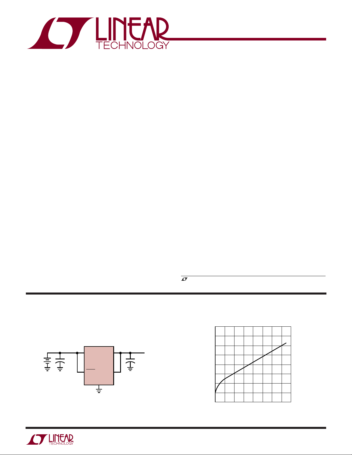
TYPICAL APPLICATION
3.3V to 2.5V Regulator
IN
> 3V
V
IN
10µF*
SHDN
OUT
LT1963A-2.5
SENSE
GND
1963 TA01
U
2.5V
++
*TANTALUM,
CERAMIC OR
ALUMINUM ELECTROLYTIC
1.5A
10µF*
Dropout Voltage
400
350
300
250
200
150
DROPOUT VOLTAGE (mV)
100
50
0
0.2
0
0.4
OUTPUT CURRENT (A)
0.6
0.8
1.0
1.2
1.4
1963 TA02
1.6
1963af
1
LT1963A Series
WWWU
ABSOLUTE AXI U RATI GS
(Note 1)
IN Pin Voltage........................................................ ± 20V
OUT Pin Voltage .................................................... ±20V
Input to Output Differential Voltage (Note 2) ......... ±20V
SENSE Pin Voltage ............................................... ±20V
ADJ Pin Voltage ...................................................... ±7V
UU
W
PACKAGE/ORDER I FOR ATIO
FRONT VIEW
5
TAB IS
GND
5-LEAD PLASTIC DD
*PIN 5 = SENSE FOR LT1963A-1.8/LT1963A-2.5/LT1963A-3.3
= ADJ FOR LT1963A
T
JMAX
4
3
2
1
Q PACKAGE
= 150∞C, qJA = 30∞C/W
SENSE/ADJ*
OUT
GND
IN
SHDN
ORDER PART
NUMBER
LT1963AEQ
LT1963AEQ-1.5
LT1963AEQ-1.8
LT1963AEQ-2.5
LT1963AEQ-3.3
ORDER PART
NUMBER
SHDN Pin Voltage................................................. ± 20V
Output Short-Circuit Duration......................... Indefinite
Operating Junction Temperature Range –45∞C to 125∞C
Storage Temperature Range ................. –65∞C to 150∞C
Lead Temperature (Soldering, 10 sec)..................300∞C
FRONT VIEW
5
4
3
2
1
TAB IS
GND
*PIN 5 = SENSE FOR LT1963A-1.8/LT1963A-2.5/LT1963A-3.3
= ADJ FOR LT1963A
T PACKAGE
5-LEAD PLASTIC TO-220
= 150∞C, qJA = 50∞C/W
T
JMAX
SENSE/ADJ*
OUT
GND
IN
SHDN
ORDER PART
NUMBER
LT1963AET
LT1963AET-1.5
LT1963AET-1.8
LT1963AET-2.5
LT1963AET-3.3
ORDER PART
NUMBER
FRONT VIEW
TAB IS
GND
ST PACKAGE
3-LEAD PLASTIC SOT-223
T
= 150∞C, qJA = 50∞C/W
JMAX
3
OUT
2
GND
1
IN
LT1963AEST-1.5
LT1963AEST-1.8
LT1963AEST-2.5
LT1963AEST-3.3
ST PART
MARKING
963A15
963A18
963A25
963A33
Consult LTC Marketing for parts specified with wider operating temperature ranges.
TOP VIEW
OUT
1
SENSE/ADJ*
*PIN 2 = SENSE FOR LT1963A-1.8/LT1963A-2.5/LT1963A-3.3
= ADJ FOR LT1963A
2
GND
3
NC
4
S8 PACKAGE
8-LEAD PLASTIC SO
= 150∞C, qJA = 70∞C/W
T
JMAX
IN
8
GND
7
GND
6
SHDN
5
LT1963AES8
LT1963AES8-1.5
LT1963AES8-1.8
LT1963AES8-2.5
LT1963AES8-3.3
S8 PART
MARKING
1963A
963A15
963A18
963A25
963A33
2
1963af
LT1963A Series
ELECTRICAL CHARACTERISTICS
The ● denotes specifications which apply over the full operating temperature range, otherwise specifications are TA = 25∞C. (Note 2)
PARAMETER CONDITIONS MIN TYP MAX UNITS
Minimum Input Voltage (Notes 4,12) I
Regulated Output Voltage (Note 5) LT1963A-1.5 VIN = 2.21V, I
ADJ Pin Voltage LT1963A VIN = 2.21V, I
(Notes 4, 5) 2.5V < V
Line Regulation LT1963A-1.5 DVIN = 2.21V to 20V, I
Load Regulation LT1963A-1.5 VIN = 2.5V, DI
Dropout Voltage I
VIN = V
OUT(NOMINAL)
(Notes 6, 7, 12)
GND Pin Current I
= V
V
IN
OUT(NOMINAL)
+ 1V I
(Notes 6, 8)
Output Voltage Noise C
ADJ Pin Bias Current (Notes 4, 9) 3 10 mA
Shutdown Threshold V
SHDN Pin Current V
(Note 10) V
Quiescent Current in Shutdown VIN = 6V, V
Ripple Rejection VIN – V
Current Limit VIN = 7V, V
= 0.5A 1.9 V
LOAD
I
= 1.5A ● 2.1 2.5 V
LOAD
= 1mA 1.477 1.500 1.523 V
2.5V < V
LT1963A-1.8 VIN = 2.3V, I
2.8V < VIN < 20V, 1mA < I
LT1963A-2.5 VIN = 3V, I
3.5V < V
LT1963A-3.3 VIN = 3.8V, I
4.3V < V
LT1963A-1.8 DV
LT1963A-2.5 DV
IN
IN
LT1963A-3.3 DVIN = 3.8V to 20V, I
LT1963A (Note 4) DV
IN
= 2.5V, DI
V
IN
LT1963A-1.8 VIN = 2.8V, DI
= 2.8V, DI
V
IN
LT1963A-2.5 VIN = 3.5V, DI
= 3.5V, DI
V
IN
LT1963A-3.3 VIN = 4.3V, DI
= 4.3V, DI
V
IN
LT1963A (Note 4) VIN = 2.5V, DI
= 2.5V, DI
V
IN
= 1mA 0.02 0.06 V
LOAD
I
= 1mA ● 0.10 V
LOAD
I
= 100mA 0.10 0.17 V
LOAD
I
= 100mA ● 0.22 V
LOAD
I
= 500mA 0.19 0.27 V
LOAD
I
= 500mA ● 0.35 V
LOAD
I
= 1.5A 0.34 0.45 V
LOAD
I
= 1.5A ● 0.55 V
LOAD
= 0mA ● 1.0 1.5 mA
LOAD
= 1mA ● 1.1 1.6 mA
LOAD
I
= 100mA ● 3.8 5.5 mA
LOAD
I
= 500mA ● 15 25 mA
LOAD
= 1.5A ● 80 120 mA
I
LOAD
= 10mF, I
OUT
= Off to On ● 0.90 2 V
OUT
= On to Off ● 0.25 0.75 V
V
OUT
= 0V 0.01 1 mA
SHDN
= 20V 3 30 mA
SHDN
OUT
= 120Hz, I
f
RIPPLE
= V
V
IN
OUT(NOMINAL)
= 1.5A, BW = 10Hz to 100kHz 40 mV
LOAD
= 0V 0.01 1 mA
SHDN
= 1.5V (Avg), V
= 0.75A
LOAD
= 0V 2 A
OUT
+ 1V, DV
LOAD
< 20V, 1mA < I
IN
= 1mA 1.773 1.800 1.827 V
LOAD
= 1mA 2.462 2.500 2.538 V
LOAD
< 20V, 1mA < I
IN
= 1mA 3.250 3.300 3.350 V
LOAD
< 20V, 1mA < I
IN
= 1mA 1.192 1.210 1.228 V
LOAD
< 20V, 1mA < I
IN
= 2.3V to 20V, I
= 3V to 20V, I
LOAD
LOAD
LOAD
= 2.21V to 20V, I
= 1mA to 1.5A 2 9 mV
LOAD
= 1mA to 1.5A ● 18 mV
LOAD
= 1mA to 1.5A 2 10 mV
LOAD
= 1mA to 1.5A ● 20 mV
LOAD
= 1mA to 1.5A 2.5 15 mV
LOAD
= 1mA to 1.5A ● 30 mV
LOAD
= 1mA to 1.5A 3 20 mV
LOAD
= 1mA to 1.5A ● 35 mV
LOAD
= 1mA to 1.5A 2 8 mV
LOAD
= 1mA to 1.5A ● 15 mV
LOAD
= 0.5V
RIPPLE
OUT
P-P
= –0.1V ● 1.6 A
< 1.5A ● 1.447 1.500 1.545 V
LOAD
< 1.5A ● 1.737 1.800 1.854 V
LOAD
< 1.5A ● 2.412 2.500 2.575 V
LOAD
< 1.5A ● 3.200 3.300 3.400 V
LOAD
< 1.5A ● 1.174 1.210 1.246 V
LOAD
= 1mA ● 2.0 6 mV
LOAD
= 1mA ● 2.5 7 mV
= 1mA ● 3.0 10 mV
= 1mA ● 3.5 10 mV
= 1mA ● 1.5 5 mV
LOAD
,5563dB
RMS
1963af
3
LT1963A Series
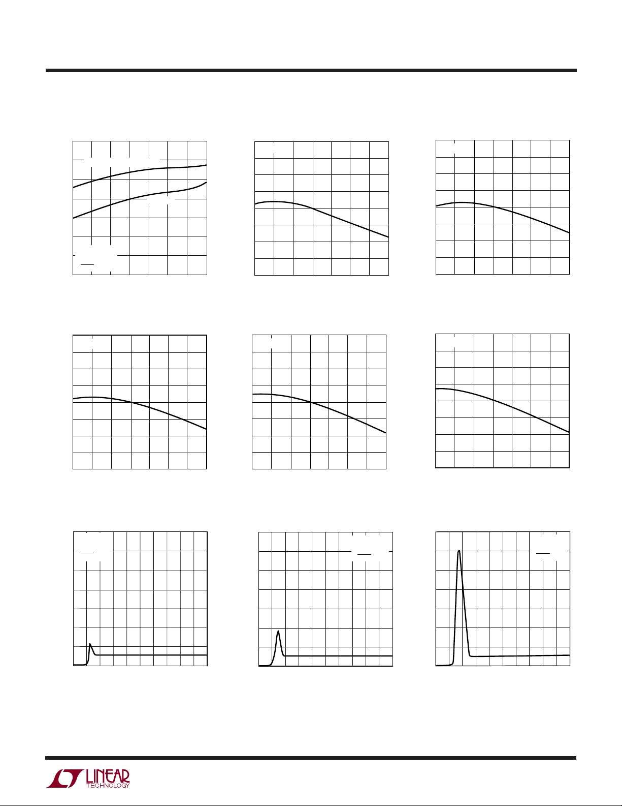
TEMPERATURE (°C)
–50
DROPOUT VOLTAGE (mV)
500
450
400
350
300
250
200
150
100
50
0
0
50
75
1963 G03
–25
25
100
125
IL = 100mA
IL = 1mA
IL = 0.5A
IL = 1.5A
ELECTRICAL CHARACTERISTICS
The ● denotes specifications which apply over the full operating temperature range, otherwise specifications are TA = 25∞C. (Note 2)
PARAMETER CONDITIONS MIN TYP MAX UNITS
Input Reverse Leakage Current (Note 13) Q, T, S8 Packages VIN = –20V, V
ST Package VIN = –20V, V
Reverse Output Current (Note 11) LT1963A-1.5 V
LT1963A-1.8 V
LT1963A-2.5 V
LT1963A-3.3 V
LT1963A (Note 4) V
= 1.5V, VIN < 1.5V 600 1200 mA
OUT
= 1.8V, VIN < 1.8V 600 1200 mA
OUT
= 2.5V, VIN < 2.5V 600 1200 mA
OUT
= 3.3V, VIN < 3.3V 600 1200 mA
OUT
= 1.21V, VIN < 1.21V 300 600 mA
OUT
= 0V ● 1mA
OUT
= 0V ● 2mA
OUT
Note 1: Absolute Maximum Ratings are those values beyond which the life
of a device may be impaired.
Note 2: Absolute maximum input to output differential voltage can not be
achieved with all combinations of rated IN pin and OUT pin voltages. With
the IN pin at 20V, the OUT pin may not be pulled below 0V. The total
measured voltage from IN to OUT can not exceed ±20V.
Note 3: The LT1963A regulators are tested and specified under pulse load
conditions such that T
TA = 25∞C. Performance at –40∞C and 125∞C is assured by design,
characterization and correlation with statistical process controls.
Note 4: The LT1963A (adjustable version) is tested and specified for these
conditions with the ADJ pin connected to the OUT pin.
Note 5: Operating conditions are limited by maximum junction
temperature. The regulated output voltage specification will not apply for
all possible combinations of input voltage and output current. When
operating at maximum input voltage, the output current range must be
limited. When operating at maximum output current, the input voltage
range must be limited.
Note 6: To satisfy requirements for minimum input voltage, the LT1963A
(adjustable version) is tested and specified for these conditions with an
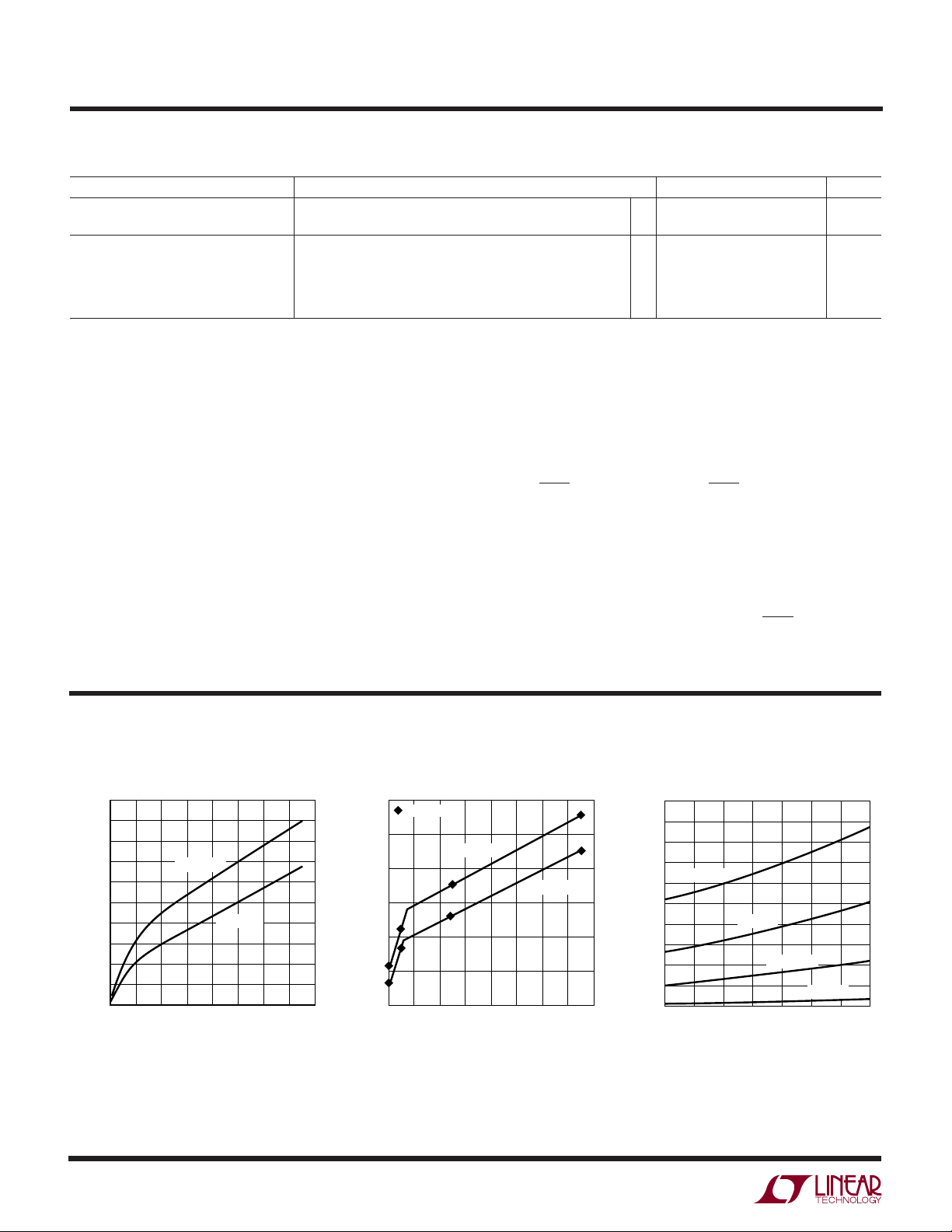
TYPICAL PERFOR A CE CHARACTERISTICS
Typical Dropout Voltage
500
450
400
350
300
250
200
150
DROPOUT VOLTAGE (mV)
100
50
0
4
0
0.2 0.6
ª TA. The LT1963A is 100% tested at
J
TJ = 125°C
TJ = 25°C
1.4
1.0
1.2
1.6
1963 • G01
0.4
0.8
OUTPUT CURRENT (A)
UW
Guaranteed Dropout Voltage
600
TEST POINTS
500
400
300
200
100
GUARANTEED DROPOUT VOLTAGE (mV)
0
0
0.2 0.6
0.4
external resistor divider (two 4.12k resistors) for an output voltage of
2.4V. The external resistor divider will add a 300mA DC load on the output.
Note 7: Dropout voltage is the minimum input to output voltage differential
needed to maintain regulation at a specified output current. In dropout, the
output voltage will be equal to: V
Note 8: GND pin current is tested with V
current source load. The GND pin current will decrease at higher input
voltages.
Note 9: ADJ pin bias current flows into the ADJ pin.
Note 10: SHDN pin current flows into the SHDN pin.
Note 11: Reverse output current is tested with the IN pin grounded and the
OUT pin forced to the rated output voltage. This current flows into the OUT
pin and out the GND pin.
Note 12. For the LT1963A, LT1963A-1.5 and LT1963A-1.8 dropout voltage
will be limited by the minimum input voltage specification under some
output voltage/load conditions.
Note 13. For the ST package, the input reverse leakage current increases
due to the additional reverse leakage current for the SHDN pin, which is
tied internally to the IN pin.
TJ ≤ 125°C
TJ ≤ 25°C
0.8
OUTPUT CURRENT (A)
1.0
1.2
1.4
1963 • G02
1.6
IN
– V
DROPOUT
= V
IN
.
OUT(NOMINAL)
Dropout Voltage
+ 1V and a
1963af
UW
TYPICAL PERFOR A CE CHARACTERISTICS
LT1963A Series
Quiescent Current
1.4
1.2
LT1963A-1.5/1.8/-2.5/-3.3
1.0
0.8
0.6
0.4
QUIESCENT CURRENT (mA)
VIN = 6V
0.2
= ∞, IL = 0
R
L
= V
V
SHDN
0
–50
IN
–25 0
25 75
TEMPERATURE (°C)
LT1963A-2.5 Output Voltage
2.58
IL = 1mA
2.56
2.54
2.52
2.50
2.48
OUTPUT VOLTAGE (V)
2.46
2.44
2.42
–50
050
–25 25 75 125
TEMPERATURE (°C)
LT1963A
50 100 125
1963 G04
100
1963 G06
LT1963A-1.5 Output Voltage
1.54
IL = 1mA
1.53
1.52
1.51
1.50
1.49
OUTPUT VOLTAGE (V)
1.48
1.47
1.46
–25 0 50
–50
25
TEMPERATURE (°C)
LT1963A-3.3 Output Voltage
3.38
IL = 1mA
3.36
3.34
3.32
3.30
3.28
OUTPUT VOLTAGE (V)
3.26
3.24
3.22
–50
050
–25 25 75 125
TEMPERATURE (°C)
75 100 125
1963 G40
100
1963 G07
LT1963A-1.8 Output Voltage
1.84
IL = 1mA
1.83
1.82
1.81
1.80
1.79
OUTPUT VOLTAGE (V)
1.78
1.77
1.76
–25 25 75 125
–50
050
TEMPERATURE (°C)
LT1963A ADJ Pin Voltage
1.230
IL = 1mA
1.225
1.220
1.215
1.210
1.205
ADJ PIN VOLTAGE (V)
1.200
1.195
1.190
–50
050
–25 25 75 125
TEMPERATURE (°C)
100
1963 G05
100
1963 G08
LT1963A-1.5 Quiescent Current
14
TJ = 25°C
= ∞
R
L
12
10
QUIESCENT CURRENT (mA)
= V
V
SHDN
IN
8
6
4
2
0
0
2
1
3
5
68
4
INPUT VOLTAGE (V)
LT1963A-1.8 Quiescent Current
14
12
10
8
6
4
QUIESCENT CURRENT (mA)
2
9
1963 G41
10
7
0
0
2
1
34
INPUT VOLTAGE (V)
TJ = 25°C
= ∞
R
L
= V
V
SHDN
IN
5678910
1963 G09
LT1963A-2.5 Quiescent Current
14
12
10
8
6
4
QUIESCENT CURRENT (mA)
2
0
0
2
1
34
INPUT VOLTAGE (V)
TJ = 25°C
= ∞
R
L
= V
V
SHDN
IN
1056789
1963 G10
1963af
5
LT1963A Series
INPUT VOLTAGE (V)
100
90
80
70
60
50
40
30
20
10
0
GND PIN CURRENT (mA)
1963 G17
0123
4
5
678910
RL = 1.8, IL = 1A*
RL = 1.2, IL = 1.5A*
RL = 3.6, IL = 500mA*
TJ = 25°C
V
SHDN
= V
IN
*FOR V
OUT
= 1.8V
UW
TYPICAL PERFOR A CE CHARACTERISTICS
LT1963A-3.3 Quiescent Current
14
12
10
8
6
4
QUIESCENT CURRENT (mA)
2
0
0
2
1
34
INPUT VOLTAGE (V)
LT1963A-1.8 GND Pin Current
25
TJ = 25°C
= V
V
SHDN
IN
*FOR V
20
15
10
GND PIN CURRENT (mA)
5
0
0
= 1.8V
OUT
RL = 18, IL = 100mA*
RL = 180, IL = 10mA*
1
3
2
INPUT VOLTAGE (V)
RL = 6, IL = 300mA*
4
TJ = 25°C
= ∞
R
L
= V
V
SHDN
IN
1963 G11
1963 G13
QUIESCENT CURRENT (mA)
1056789
GND PIN CURRENT (mA)
1098765
LT1963A Quiescent Current
14
12
10
8
6
4
2
0
0
4
2
68
INPUT VOLTAGE (V)
LT1963A-2.5 GND Pin Current
25
20
15
10
5
0
0
RL = 8.33, IL = 300mA*
RL = 25, IL = 100mA*
RL = 250, IL = 10mA*
1
3
2
INPUT VOLTAGE (V)
TJ = 25°C
V
SHDN
*FOR V
4
TJ = 25°C
= 4.3k
R
L
= V
V
SHDN
= V
IN
= 2.5V
OUT
IN
1963 G12
1963 G14
GND PIN CURRENT (mA)
2010 12 14 16 18
GND PIN CURRENT (mA)
1098765
LT1963A-1.5 GND Pin Current
25
TJ = 25°C
= V
V
SHDN
IN
*FOR V
20
15
10
5
0
0
= 1.5V
OUT
RL = 150, IL = 10mA*
123
45
INPUT VOLTAGE (V)
RL = 5, IL = 300mA*
RL = 15, IL = 100mA*
67 9
LT1963A-3.3 GND Pin Current
25
20
15
10
5
0
0
RL = 330, IL = 100mA*
1
3
2
INPUT VOLTAGE (V)
TJ = 25°C
V
SHDN
*FOR V
RL = 11, IL = 300mA*
RL = 33, IL = 100mA*
4
= V
OUT
8
IN
= 3.3V
10
1963 G42
1098765
1963 G15
10
8
6
4
GND PIN CURRENT (mA)
2
0
6
LT1963A GND Pin Current
TJ = 25°C
= V
V
SHDN
*FOR V
RL = 4.33, IL = 300mA*
RL = 12.1, IL = 100mA*
RL = 121, IL = 10mA*
1
0
2
3
4
INPUT VOLTAGE (V)
OUT
IN
= 1.21V
1963 G16
LT1963A-1.8 GND Pin CurrentLT1963A-1.5 GND Pin Current
100
90
80
70
60
50
40
30
GND PIN CURRENT (mA)
20
10
1098765
0
0
RL = 1, IL = 1.5A*
21
INPUT VOLTAGE (V)
TJ = 25°C
V
SHDN
*FOR V
RL = 1.5, IL = 1A*
RL = 3, IL = 500mA*
67 9
43
5
= V
OUT
IN
= 1.5V
8
10
1963 G43
1963af
 Loading...