

Page 1

LOAD CURRENT (A)
0.5
EFFICIENCY (%)
95
90
85
80
75
70
4.5
1950 TA01b
1.5
2.5
3.5
5.5
VIN = 48V
VIN = 36V
VIN = 72V
FEATURES
LT1950
Single Switch PWM
Controller with Auxiliary
Boost Converter
U
DESCRIPTIO
■
Wide Input Range: 3V to 25V
■
Programmable Volt-Second Clamp
■
Output Power Levels from 25W to 500W
■
Auxiliary Boost Converter Provides 10V Gate Drive
from VIN as Low as 3V
■
Programmable Operating Frequency (100kHz to
500kHz) with One External Resistor
■
Programmable Slope Compensation
■
Programmable Leading Edge Blanking
■
±2% Internal 1.23V Reference
■
Accurate Shutdown Pin Threshold with
Programmable Hysteresis
■
60ns Current Sense Delay
■
2.5V Auxiliary Reference Output
■
Synchronizable to an External Clock up to 1.5 • f
■
Current Mode Control
■
Small 16-Pin SSOP Package
U
APPLICATIO S
■
Telecom Power Supplies
■
Automotive Power Supplies
■
Portable Electronic Equipment
■
Isolated and Nonisolated DC/DC Converters
OSC
The LT®1950 is a wide input range, forward, boost, flyback
and SEPIC controller that drives an N-channel power
MOSFET with few external components required.
A resistor programmable duty cycle clamp can be used to
generate a volt-second clamp for forward converter applications. An internal boost switcher is available for creating
a separate supply for the output gate driver, allowing 10V
gate drive from input voltages as low as 3V. The LT1950’s
operating frequency can be set with an external resistor
over a 100kHz to 500kHz range and a SYNC pin allows the
part to be synchronized to an external clock. Additional
programmability exists for leading edge blanking and
slope compensation.
A fast current sense comparator achieves 60ns current
sense delay and the error amplifier is a true voltage mode
error amplifier, allowing a wide range of compensation
networks. An accurate shutdown pin with programmable
hysteresis is available for undervoltage lockout and shutdown. The LT1950 is available in a small 16-Pin SSOP
package.
, LTC and LT are registered trademarks of Linear Technology Corporation.
TYPICAL APPLICATIO
2.5V
0.1µF
249k
4.99k
U
36V to 72V DC to 26V/5A (Single Switch) Forward Converter
SLOPE
V
REF
BOOST
R
OSC
LT1950
BLANK
SYNC
GND
FB
V
V
SHDN
GATE
I
SENSE
PGND
COMP
V
IN2
SEC
10V
BIAS
IN
1µF
4.7k
0.022µF
470k
18k
100k
V
IN
MBRB20200
PA0581
Si7450
0.015Ω
47µH
47µF
1950 TA01a
V
26V
5A
Efficiency vs Load Current
OUT
1950fa
1
Page 2
LT1950
TOP VIEW
GN PACKAGE
16-LEAD NARROW PLASTIC SSOP
1
2
3
4
5
6
7
8
16
15
14
13
12
11
10
9
COMP
FB
R
OSC
SYNC
SLOPE
V
REF
SHDN
GND
V
SEC
V
IN
BOOST
PGND
GATE
V
IN2
I
SENSE
BLANK
ABSOLUTE AXI U RATI GS
(Note 1)
BOOST ....................................................... –0.3V to 35V
V
, V
IN
FB, SYNC, V
COMP, BLANK ..........................................–0.3V to 3.5V
SLOPE ...................................................... –0.3V to 2.5V
I
SENSE
R
OSC
V
REF
Operating Junction Temperature Range
LT1950EGN/LT1950IGN (Notes 2, 5) ... –40°C to 125°C
Storage Temperature Range ..................–65°C to 150°C
Lead Temperature (Soldering, 10 sec).................. 300°C
ELECTRICAL CHARACTERISTICS
temperature range, otherwise specifications are at TA = 25°C. COMP = open, FB = 1.4V, R
= 0.1µF, SHDN = VIN, BLANK = 0V, I
specified.
PARAMETER CONDITIONS MIN TYP MAX UNITS
PWM Controller
Operating Input Voltage I
Minimum Start-Up Voltage I
VIN Quiescent Current I
V
Shutdown Current SHDN = 0V 5 20 µA
IN
Shutdown Threshold 3V < V
Shutdown Pin Current SHDN = 70mV Above Threshold –7 –10 –13 µA
Shutdown Pin Current Hysteresis SHDN = 100mV Below Threshold 4 7 10 µA
V
Quiescent Current I(V
IN2
V
Shutdown Current SHDN = 0V, V
IN2
V
(External Output)
REF
Output Voltage I
Line Regulation I
Load Regulation 0µA < I
Oscillator
Frequency: f
Minimum Programmable f
Maximum Programmable f
SYNC Input Resistance 20 kΩ
SYNC Switching Threshold 1.5 2.2 V
SYNC Frequency/f
f
OSC
V
ROSC
2
Line Reg 3V < VIN < 25V 0.05 0.15 %/V
WW
W
, SHDN ......................................... –0.3V to 25V
IN2
........................................... –0.3V to 6V
SEC
U
......................................................... –0.3V to 1V
.................................................................... –50µA
.................................................................... –10mA
The ● denotes the specifications which apply over the full operating
= 0V, V
SENSE
OSC
OSC
OSC
OSC
= 15V, GATE = 1nF, BOOST = open, VIN = 15V, V
IN2
= 0µA ● 3.0 25 V
VREF
= 0µA ● 2.6 3.0 V
VREF
= 0µA, FB = 1V, I
VREF
< 25V ● 1.261 1.32 1.379 V
IN
) = 0µA, FB = 1V, I
REF
= 2.7V (Boost Diode from VIN = 3V) 500 700 µA
IN2
= 0µA ● 2.425 2.500 2.575 V
VREF
= 0µA, 3V < VIN < 25V 1 5 mV
VREF
< 2.5mA 1 5 mV
VREF
R
= 249k, FB = 1V ● 170 200 230 kHz
OSC
R
= 499k 85 100 115 kHz
OSC
R
= 90.9k 440 500 560 kHz
OSC
(R
= 249k, f
OSC
9.5V < V
IN2
=200kHz), FB = 1V (Note 7) 1.25 1.5
OSC
< 25V 0.05 0.25 %/V
UUW
PACKAGE/ORDER I FOR ATIO
ORDER PART
NUMBER
LT1950EGN
LT1950IGN
GN PART MARKING
1950E
T
= 125°C, θJA = 110°C/W,
JMAX
(PIN 8) = 30°C/W
θ
JC
Consult LTC Marketing for parts specified with wider operating temperature ranges.
= 249k, SYNC = 0V, SLOPE = open, V
OSC
= 0.2V 2.3 3.0 mA
SENSE
= 0.2V 1.7 2.5 mA
SENSE
= 0V, unless otherwise
SEC
1950I
1V
REF
1950fa
Page 3
LT1950
ELECTRICAL CHARACTERISTICS
temperature range, otherwise specifications are at TA = 25°C. COMP = open, FB = 1.4V, R
= 0.1µF, SHDN = VIN, BLANK = 0V, I
SENSE
= 0V, V
IN2
The ● denotes the specifications which apply over the full operating
= 249k, SYNC = 0V, SLOPE = open, V
= 15V, GATE = 1nF, BOOST = open, VIN = 15V, V
OSC
= 0V, unless otherwise
SEC
REF
specified.
PARAMETER CONDITIONS MIN TYP MAX UNITS
Error Amplifier
FB Reference Voltage 3V < VIN < 25V, V
FB Input Bias Current FB = FB Reference Voltage –75 –200 nA
Open Loop Voltage Gain VOL + 0.2V < COMP < VOH – 0.2 65 85 dB
Unity Gain Bandwidth (Note 6) 3 MHz
COMP Source Current FB = 1V, COMP = 1.6V ● –0.3 –1.1 –1.8 mA
COMP Sink Current FB = 1.4V, COMP = 1.6V 8 13 mA
COMP High Level: V
OH
FB = 1V, I
COMP
COMP Active Threshold Start of GATE Switching (Duty Cycle > 0%) 1.0 V
COMP Low Level: V
OL
FB = 1.4V, I
Current Sense
I
Maximum Threshold Duty Cycle < 10%, COMP = V
SENSE
I
Input Bias Current COMP = 2.5V, I
SENSE
Default Blanking Time FB = 1V, COMP = 2V, I
Adjustable Blanking Time FB = 1V, COMP = 2V, I
BLANK = 75k to Ground
Blanking Override Voltage– BLANK = Open, COMP = 2.5V (Note 4) 15 25 40 mV
Maximum Threshold
I
SENSE
Turn-Off Delay to Gate COMP = 2V 60 ns
Slope Compensation (Note 4) I
Max Threshold (DC < 10%) – (DC = 80%) (Note 4)
SENSE
Default, R
SLOPE
2x Default, R
3x Default, R
Internal Switcher
Boost Switch I
LIMIT
Boost Switch Off Time V
V
: Boost Disable 3V < VIN < 10V ● 9.5 11.0 11.75 V
IN2
V
: Boost Disable Hysteresis 3V < VIN < 10V –1.0 V
IN2
V
: Gate Enable 3V < VIN < 10V, FB = 1V (Note 4) ● 7.0 8.2 9.27 V
IN2
V
: Gate Enable Hysteresis 3V < VIN < 10V, FB = 1V (Note 4) –0.6 V
IN2
V
= 8V, 3V < VIN < 10V 70 125 180 mA
IN2
= 8V, 3V < VIN < 10V 250 500 1000 ns
IN2
GATE Driver Output
GATE Rise Time FB = 1V, V
GATE Fall Time FB = 1V, V
GATE Clamp Voltage I
GATE Low Level I
GATE High Level I
GATE
GATE
I
GATE
GATE
I
GATE
Maximum Duty Cycle FB = 1V, f
IN2
IN2
= 0µA, COMP = 2.5V, FB = 6V 11.5 13 14.5 V
= 20mA 0.25 0.4 V
= 200mA 1.2 1.75 V
= –20mA, V
= –200mA, V
OSC
+ 0.2V < COMP < VOH – 0.2 ● 1.205 1.230 1.254 V
OL
= – 250µA 2.5 V
= 250µA 0.15 V
COMP
90 100 110 mV
SENSE
OH
= I
Max Threshold –125 –170 –250 µA
SENSE
= 75mV 110 ns
SENSE
= 75mV 290 ns
SENSE
= ∞ 14 mV
= 8k 28 mV
SLOPE
= 3.3k 42 mV
SLOPE
= 12V, CL = 1nF (Notes 3, 6) 50 ns
= 12V, CL = 1nF (Notes 3, 6) 30 ns
= 12V, COMP = 2.5V, FB = 6V 10 V
IN2
= 12V, COMP = 2.5V, FB = 6V 9.75 V
IN2
= 200kHz 90 95 97 %
1950fa
3
Page 4
LT1950
ELECTRICAL CHARACTERISTICS
temperature range, otherwise specifications are at TA = 25°C. COMP = open, FB = 1.4V, R
= 0.1µF, SHDN = VIN, BLANK = 0V, I
SENSE
= 0V, V
IN2
The ● denotes the specifications which apply over the full operating
= 249k, SYNC = 0V, SLOPE = open, V
= 15V, GATE = 1nF, BOOST = open, VIN = 15V, V
OSC
= 0V, unless otherwise
SEC
REF
specified.
PARAMETER CONDITIONS MIN TYP MAX UNITS
Maximum Duty Cycle Clamp V
V
Input Bias Current 0V < V
SEC
Note 1: Absolute Maximum Ratings are those values beyond which the life
of a device may be impaired.
Note 2: The LT1950EGN is guaranteed to meet performance specifications
from 0°C to 125°C operating junction temperature. Specifications over the
–40°C to 125°C operating junction temperature range are assured by
design, characterization and correlation with statistical process controls.
The LT1950IGN is guaranteed over the full –40°C to 125°C operating
junction temperature range.
= 1.4V, FB = 1V, COMP = V
SEC
< 2.8V –0.3 –1.0 µA
SEC
OH
63 75 87 %
Note 4: Guaranteed by correlation to static test.
Note 5: This IC includes overtemperature protection that is intended to
protect the device during momentary overload conditions. Junction
temperature will exceed 125°C when overtemperature protection is active.
Continuous operation above the specified maximum operating junction
temperature may impair device reliability.
Note 6: Guaranteed but not tested.
Note 7: Maximum recommended SYNC frequency = 500kHz.
Note 3: Rise and Fall times are between 10% and 90% levels.
UW
TYPICAL PERFOR A CE CHARACTERISTICS
Switching Frequency vs
FB Voltage vs Temperature
1.26
1.25
1.24
1.23
FB VOLTAGE (V)
1.22
1.21
1.20
–50
–25 0
25 75
TEMPERATURE (°C)
50 100 125
1950 G01
Temperature
240
230
220
210
200
190
FREQUENCY (kHz)
180
170
160
–25 25 75
–50
0
TEMPERATURE (°C)
50
100
1950 • G02
125
VIN Shutdown IQ vs Temperature
16
SHDN = 0V
14
12
(µA)
Q
10
8
6
SHUTDOWN I
IN
V
4
2
0
–25 25 75
–50
0
TEMPERATURE (°C)
50
100
125
1950 • G03
Shutdown Threshold vs
Temperature
1.45
1.40
1.35
1.30
SHUTDOWN THRESHOLD (V)
1.25
1.20
–25 25 75
–50
0
TEMPERATURE (°C)
4
I
Maximum I
Threshold vs
SENSE
Temperature
125
120
115
110
105
THRESHOLD (mV)
100
95
SENSE
90
85
MAXIMUM I
80
50
100
125
1950 • G04
75
–50
0
–25
TEMPERATURE (°C)
50
25
75
100
125
1950 G05
270
250
230
210
190
170
CURRENT (µA)
150
SENSE
I
130
110
90
Pin Current vs
SENSE
Temperature
–50 0
–25
50
25
TEMPERATURE (°C)
100
125
1950 G06
1950fa
75
Page 5
UW
TYPICAL PERFOR A CE CHARACTERISTICS
BLANK Override Threshold –
I
Maximum Threshold vs
SENSE
Temperature
40
35
30
25
20
MAXIMUM THRESHOLD (mV)
BLANK OVERRIDE THRESHOLD
15
SENSE
–I
10
–50
–25 0
25 75
TEMPERATURE (°C)
50 100 125
1950 G07
Minimum VIN Start-Up Voltage vs
Temperature (V
3.00
2.75
2.50
START-UP VOLTAGE (V)
IN
2.25
MINIMUM V
2.00
–25 25 75 125
–50
050
TEMPERATURE (°C)
Boosted)
IN2
100
1950 G08
3.1
2.9
2.7
2.5
(mA)
2.3
Q
I
IN
V
2.1
1.9
1.7
1.5
LT1950
V
vs Temperature
IN IQ
050
–25 25 75 125
–50
TEMPERATURE (°C)
100
1950 G09
SHDN Input Current *(–1) vs
Temperature
14
12
SHDN = SHDN THRESHOLD + 70mV
10
8
6
4
SHDN = SHDN THRESHOLD – 100mV
SHDN INPUT CURRENT*(–1) (µA)
2
0
–50 25 75
–25 0
TEMPERATURE (°C)
V
: GATE Enable
IN2
vs Temperature
9.2
8.7
GATE ENABLE
8.2
GATE ENABLE (V)
IN2
V
7.7
7.2
–50 25 75
–25 0
HYSTERESIS
GATE DISABLE
TEMPERATURE (°C)
50 100 125
1950 G10
50 100 125
1950 G13
SHDN Current Hysteresis vs
Temperature
11
10
9
8
7
6
5
SHDN CURRENT HYSTERESIS (µA)
4
3
–50
V
IN2
050
–25 25 75 125
TEMPERATURE (°C)
: BOOST Disable
vs Temperature
13.0
12.5
12.0
11.5
11.0
10.5
BOOST DISABLE (V)
IN2
V
10.0
9.5
9.0
–50
BOOST DISABLE
HYSTERESIS
BOOST RE-ENABLE
–25 25 75
0
TEMPERATURE (°C)
GATE Rise/Fall Time vs
GATE Capacitance
125
TA = 25°C
100
1950 G11
100
75
50
GATE RISE/FALL TIME (ns)
25
0
1000
0
BOOST Switch I
t
r
t
f
3000
2000
GATE CAPACITANCE (pF)
vs
LIMIT
4000
5000
1950 G12
Temperature
250
200
(mA)
LIMIT
150
100
BOOST SWITCH I
50
100
125
1950 G14
50
–50 25 75
–25 0
TEMPERATURE (°C)
50 100 125
1950 G15
1950fa
5
Page 6
LT1950
UW
TYPICAL PERFOR A CE CHARACTERISTICS
BOOST Switch Off Time vs
Temperature
700
600
500
400
BOOST SWITCH OFF TIME (ns)
300
–50 25 75
–25 0
TEMPERATURE (°C)
U
50 100 125
1950 G16
UU
Maximum Duty Cycle vs
Voltage
V
SEC
100
90
80
70
60
50
MAXIMUM DUTY CYCLE (%)
40
30
0.8
MAX DUTY CYCLE = (105/V
1.25V < V
= 25°C
T
A
1.6 2.0 2.4 2.8 3.2
1.2
V
SEC
PI FU CTIO S
COMP (Pin 1): The COMP pin is the output of the error
amplifier. The error amplifier is a true op amp which allows
the use of an RC network to be connected between the
Comp and FB pins to compensate the feedback loop for
optimum transient response. The peak switch current in
the external MOSFET will be proportional to the voltage on
the COMP pin. Typical operating voltage range for this pin
is 1V to 2.5V.
FB (Pin 2): The FB pin is the inverting input to the error
amplifier. The output voltage is set with a resistor divider.
The error amplifier adjusts the peak switch current to
maintain the FB pin voltage at the value of the internal
reference voltage of 1.23V.
R
(Pin 3): A resistor from the R
OSC
programs the operating frequency of the LT1950. Operating frequency range is 100kHz to 500kHz. Nominal voltage
on the R
pin is 1V.
OSC
pin to ground
OSC
GATE Clamp Voltage vs
Temperature
16
15
14
13
12
GATE CLAMP VOLTAGE (V)
11
10
–50
050
–25 25 75 125
TEMPERATURE (°C)
100
1950 G18
< 2.8V
SEC
VOLTAGE (V)
SEC
)%
1950 G17
SLOPE (Pin 5): The SLOPE pin is used to adjust the
amount of slope compensation. Leaving the pin open
circuit results in a default level of slope compensation. The
amount of slope compensation can be adjusted above this
default level by connecting a resistor from the SLOPE pin
to the V
V
REF
pin.
REF
(Pin 6): The V
pin is the output of an internal 2.5V
REF
reference. This pin is capable of sourcing up to 2.5mA for
external use. It is recommended that the V
REF
pin is
bypassed to ground with a 0.1µF ceramic capacitor.
SHDN (Pin 7): The SHDN pin is used to put the device into
a low power shutdown state. In shutdown the VIN supply
current drops to 5µA. The SHDN pin has an accurate
threshold of 1.32V which can be used to program an
undervoltage lockout threshold. Input current levels on
the SHDN pin can be used to program hysteresis into the
undervoltage lockout levels.
SYNC (Pin 4): The SYNC pin is used to synchronize the
internal oscillator to an external clock signal. The pin is
directly logic compatible and can be driven with any signal
with a duty cycle of 10% to 90%. If the SYNC function is
not used the pin can be left open circuit or connected to
ground.
6
GND (Pin 8): The GND pin is the analog ground for the
internal circuitry of the LT1950. Sensitive circuitry such as
the feedback divider, frequency setting resistor, reference
bypass capacitor should be tied directly to this pin. See the
Applications Information section for recommendations
on ground connections.
1950fa
Page 7

LT1950
U
UU
PI FU CTIO S
BLANK (Pin 9): The BLANK pin is used to adjust the
leading edge blanking period of the current sense amplifier
during FET turn-on. Shorting the BLANK pin to ground
provides a default blanking period of approximately 110ns.
A resistor from the BLANK pin to ground increases the
blanking period up to 290ns for R
I
(Pin 10): The I
SENSE
pin is the current sense input
SENSE
for the control loop. Connect this pin to the sense resistor
in the source of the external power MOSFET.
V
(Pin 11): The V
IN2
pin is the supply pin for the
IN2
MOSFET gate drive circuit. Power can be supplied to this
pin by an external supply such as VIN, and must exceed 8V
(the undervoltage lockout threshold for the gate driver
supply). For low VIN supply voltages an internal boost
regulator can be used to generate as much as 11V at the
V
pin. This allows the LT1950 to run with VIN supply
IN2
voltages down to 3V while still supplying enough gate
drive for standard level MOSFETs.
GATE (PIN 12): The GATE pin is the output of a high current
gate drive circuit used to drive an external MOSFET. The
output is actively clamped to a max voltage of 13V if V
is supplied by a high voltage.
PGND (Pin 13): This is the ground connection for the high
current gate driver stage. See the Applications Information section for recommendations on ground connections.
BLANK
= 75k.
IN2
BOOST (Pin 14): The BOOST pin is the NPN collector
output of the internal boost converter which can be used
to generate an 11V supply for the MOSFET gate driver
circuit. The boost converter runs with a fixed off-time of
0.5µs and a current limit of 125mA. The converter runs
until the V
the V
IN2
voltage exceeds 11V and then turns off until
IN2
voltage drops below 10V. If the V
voltage is
IN2
supplied externally, the BOOST pin should be shorted to
ground or left open.
VIN (Pin 15): The VIN pin is the main supply pin for the
LT1950. This pin must be closely bypassed to ground. If
V
is generated using the BOOST pin then the LT1950
IN2
will be fully functional, internal V
will be active and the
REF
gate output will be enabled with a VIN voltage as low as 3V.
An internal undervoltage lockout threshold exists at approximately 2.6V on the VIN pin. Undervoltage lockout
voltages greater than 3V can be programmed using a
voltage divider on the SHDN pin.
V
(Pin 16): The V
SEC
pin is used to program the
SEC
maximum duty cycle of the gate driver circuit. The maximum duty cycle will be equal to (105/V
)% for V
SEC
SEC
between 1.4V and 2.8V. This is a useful function to limit the
flyback voltage in a forward converter. If the maximum
duty cycle function is not used then the V
pin should be
SEC
tied to ground.
1950fa
7
Page 8

LT1950
BLOCK DIAGRA
W
SHDN
SYNC
R
OSC
SLOPE
V
IN
15 16 14
1.23V
–
+
1.32V
3µA
7
4
3
5
1.23V
+
(TYPICAL 200kHz)
OSC
ERROR AMPLIFIER
VOLTAGE GAIN = 85dB
V
REF
V
IN2
V
=
REF
INTERNAL +
EXTERNAL
SUPPLY
2.5V
(SOURCE 2.5mA
EXTERNALLY)
(V
) (2.6V)
IN
U/V LOCKOUT
(100-500)khz
6
(105/V
RAMP
–
V
SEC
SEC
)%
BOOST
SWITCHING PREREGULATOR
(125mA CURRENT LIMIT)
PGND
–
MAX DC
CLAMP
+
SLOPE COMP
CURRENT
SENSE
0mV – >100mV
FIXED OFF TIME
S
R
BLANKING
CMP
–
DISABLE
(V
) (8V)
IN2
U/V LOCKOUT
ENABLE
–
Q
+
+
±1A
DRIVER
+
–
+
–
13V
–
125mV
11V
8V
BLANKING
OVERRIDE
CMP
+
V
IN2
11
12
GATE
13
PGND
10
I
SENSE
FB COMP GND BLANK
81 92
Figure 1. LT1950 Block Diagram
U
OPERATIO
The LT1950 is a constant frequency, current mode controller for DC/DC forward, boost, flyback and SEPIC converter applications. The Block Diagram in Figure 1 shows
all of the key functions of the IC.
In normal operation, a VIN voltage as low as 3V allows an
internal switcher at the BOOST pin to generate a separate
8
1950 BD
11V supply at V
inductor, diode and capacitor. Since V
using a small surface mount external
IN2
supplies the
IN2
output driver of the IC, this architecture achieves high
GATE drive for an external N-channel power MOSFET even
though VIN voltage is very low. High GATE drive capability
reduces MOSFET R
for improved efficiency,
DS(ON)
1950fa
Page 9

OPERATIO
LT1950
U
increases the range of MOSFETs that can be selected and
allows applications requiring high gate drive with a large
swing in V
voltage. When V
IN
exceeds 8V, the GATE
IN2
output driver is enabled. The GATE switches between 0V
and V
R
OSC
at a constant frequency set by a resistor from the
IN2
pin to ground. When V
reaches 11V, the internal
IN2
switcher at the BOOST pin is disabled to save power and
only re-enabled when V
drops below 10V. The internal
IN2
boost switcher runs in burst mode operation, asynchronous to the main oscillator. If low VIN operation with high
GATE drive is not required, the BOOST pin is left open and
the V
pin shorted to VIN. With V
IN2
minimum operational V
8V (required at V
to enable the GATE output driver). For
IN2
voltage will increase from 3V to
IN
shorted to VIN the
IN2
GATE turn on, a PWM latch is set at the start of each main
oscillator cycle. For GATE turn off, the PWM latch is reset
when either the current sense comparator is tripped, the
maximum duty cycle is reached, or the BLANK override
threshold is exceeded.
A resistor divider from the application’s output voltage
generates a voltage at the FB pin that is compared to the
internal 1.23V reference by the error amplifier. The error
amplifier output (COMP) defines the input threshold
(I
voltage is clamped to 100mV. By connecting I
) of the current sense comparator. Maximum I
SENSE
SENSE
SENSE
to a
sense resistor in series with the source of the external
MOSFET, the peak switch current is controlled by COMP.
An increase in output load current causing the output
voltage to fall, will cause COMP to rise, increasing I
SENSE
threshold, increasing the current delivered to the output.
This current mode technique means that the error amplifier commands current to be delivered to the output rather
than voltage. This makes frequency compensation easier
and provides faster loop response to output load transients.
The current mode architecture requires slope compensation to be added to the current sensing loop to prevent
subharmonic oscillations which can occur for duty cycles
above 50%. Unlike most current mode converters which
have a slope compensation ramp that is fixed internally,
placing a constraint on inductor value and operating
frequency, the LT1950 has externally adjustable slope
compensation. A default level of slope compensation is
achieved with the SLOPE pin open. Increased slope compensation can be programmed by reducing the value of
resistance inserted between the SLOPE pin and V
REF
pin.
A SYNC pin allows the LT1950 main oscillator to be
synchronized to an external clock . To avoid loss of slope
compensation during synchronization, the free running
main oscillator frequency should be programmed to approximately 80% of the external clock frequency.
The LT1950 can be placed into shutdown mode when the
SHDN pin drops below an accurate 1.32V threshold. This
threshold can be used to program undervoltage lockout
(UVLO) at VIN for current limited or high source resistance
supplies. SHDN pin current hysteresis also exists to allow
external programming of UVLO voltage hysteresis. When
VIN and V
and 6.8V, the V
exceed internally set UVLO thresholds of 2.6V
IN2
output becomes active. The V
REF
REF
output
is a 2.5V reference supplying the majority of LT1950
control circuitry and capable of sourcing up to 2.5mA for
external use.
To prevent noise in the system causing premature turn off
of the external MOSFET the LT1950 has leading edge
blanking. This means the current sense comparator output is ignored during MOSFET turn on and for an extended
period after turn on. The extended blanking period is
adjusted by inserting a resistor from the BLANK pin to
ground. A short to ground defines a minimum default
blanking period. Increased resistance from the BLANK pin
to ground will increase blanking duration. Fault conditions
causing I
and reduce the I
to exceed 125mV will override blanking
SENSE
to GATE delay to 60ns.
SENSE
For applications requiring maximum duty cycle clamping,
the V
the pin. The V
pin reduces duty cycle for increased voltage on
SEC
pin provides a volt-second clamp critical
SEC
in forward converter applications.
Maximum duty cycle follows (105/V
ages between 1.4V to 2.8V. If unused, the V
)% for V
SEC
SEC
pin should
SEC
volt-
be shorted to ground, leaving the natural maximum duty
cycle of the part to be typically 95% for 200kHz operation.
1950fa
9
Page 10

LT1950
U
WUU
APPLICATIO S I FOR ATIO
LT1950 Input Supplies, V
is the main input supply for the LT1950. V
V
IN
input supply for the LT1950 output driver. V
provided by shorting the V
generating V
V
, V
IN2
REF
using the BOOST pin. Waveforms of VIN,
IN2
and GATE switching are shown in Figures 2 and
3. Figure 2 represents low VIN operation with V
ated using the B00ST pin. Figure 3 represents VIN = V
operation with the BOOST pin open circuit or shorted to
ground.
Low VIN Operation
The LT1950 can be configured to provide a minimum of
10V GATE drive for an external N-channel MOSFET from
VIN voltages as low as 3V, if the BOOST pin is used to
generate a second supply at the V
Applications Information “ Generating V
BOOST Pin”). The advantage of this configuration is that a
lower R
is achieved for the external N-channel
DS(ON)
MOSFET, improving efficiency, versus a controller running at 3V input without boosted gate drive. In addition,
typical controllers running at low input voltages have the
limitation of only being able to use logic level MOSFETs.
The LT1950 allows a greater range of usable MOSFETs.
This versatility allows optimization of the overall power
supply performance and allows applications which would
otherwise not be possible without a more complex topology. Figure 2 shows that for VIN above 2V, the internal
switcher at the BOOST pin is enabled. This switch generates the V
supply. As V
IN2
undervoltage lockout threshold of 6.8V the 2.5V reference
V
becomes active and powers up internal control
REF
circuitry. When V
driver is enabled. V
exceeds approximately 8V, the gate
IN2
is regulated between 10V and 11V,
IN2
providing a supply to the LT1950 output driver to ensure
a minimum of 10V drive at the GATE pin.
Output and GATE Enable
REF
IN2
IN2
pin to the VIN pin or by
IN2
IN2
pin (see Figure 2 and
IN2
Supply Using
IN2
ramps up above the
IN2
is the
can be
gener-
IN2
VIN = V
Operation
IN2
If low VIN operation is not required below approximately
8V on VIN the LT1950 can be configured to run without the
use of the BOOST pin by shorting the V
pin. Figure 3 shows that both VIN and V
exceed 6.8V to activate the 2.5V V
REF
pin to the V
IN2
IN2
must now
IN
output and must
exceed approximately 8V to enable the output driver
(GATE pin).
12
V
IN2
GATE
IN2
10µs/DIV
Figure 3. VIN = V
MIN
3V
V
IN
V
REF
50µs/DIV
Figure 2. Low VIN Operation
TYPICAL START-UP INPUT
Operation
IN2
IN2
IN2
V
V
>8.2V
IN2
IN2
L1
D1
C1
*
C1
V
IN
BOOST
BOOST
LT1950
V
V
V
IN
BOOST
BOOST
LT1950
*BOOST PIN CAN BE
LEFT OPEN OR
SHORTED TO GROUND
1950 F02
1950 F03
10.2
8.5
6.8
5.1
3.4
5.0
2.5
8
4
0
4
3
2
1
0
VIN = V
V
REF
0
10
GATE
5
0
10
1950fa
Page 11

LT1950
U
WUU
APPLICATIO S I FOR ATIO
Shutdown and Undervoltage Lockout
Figure 4 shows how to program undervoltage lockout
(UVLO) for the V
situations where the input supply is current limited, or has
a relatively high source resistance. A switching regulator
draws constant power from the source, hence source
current increases as source voltage drops. This looks like
a negative load resistance to the source and can cause the
source to current limit or latch low under low source
voltage conditions. An internally set undervoltage lockout
(UVLO) threshold prevents the regulator from operating at
source voltages where these problems might occur. An
internal comparator will force the part into shutdown
below the minimum VIN of 2.6V. This feature can be used
to prevent excessive discharge of battery-operated systems. Alternatively, UVLO threshold is adjustable. The
shutdown threshold voltage of the SHDN pin is 1.32V.
Forcing the SHDN pin below this 1.32V threshold causes
V
to be disabled and stops switching at the GATE pin.
REF
If the SHDN pin is left open circuit, a permanent 3µA flows
out of the pin to ensure that the pin defaults high to allow
normal operation. Voltages above the 1.32V threshold
cause an extra 7µA to be sourced out of the pin, providing
current hysteresis. This can be used to set voltage hysteresis of the UVLO threshold using the following equations:
supply. Typically, UVLO is used in
IN
Example: switching should not start until the input is
above 11V and is to stop if the input falls below 9V.
= 11V
V
H
V
= 9V
L
VV
11 9
R
1
R
2
–
=
7
=
11 1 32
(–.)
=
A
µ
132
.
VV
k
286
286
V
k
A
3
+µ
k
36
=
Keep the connections from the resistors to the SHDN pin
short and make sure that the interplane or surface capacitance to the switching nodes are minimized. If high resistance values are used, the SHDN pin should be bypassed
with a 1nF capacitor to prevent coupling problems from
the switch node.
LT1950
V
IN
R1
C1
R2
3µA
1.32V
7µA
GND
V
REF
+
VV
–
HL
R
1
=
A
7
µ
V
132
R
2
=
VV
(–. )
.
132
H
R
1
3
+µ
VH = Turn on threshold
VL = Turn off threshold
1950 F04
Figure 4. Undervoltage Lockout
Generating V
A
The LT1950’s BOOST pin is used to provide a “boosted”
11V supply at the V
Since V
IN2
the IC, it is advantageous to generate a boosted V
Supply Using BOOST Pin
IN2
pin for VIN voltages as low as 3V.
IN2
supplies the output driver for the GATE pin of
. This
IN2
architecture achieves high GATE drive for an external
1950fa
11
Page 12

LT1950
U
WUU
APPLICATIO S I FOR ATIO
N-channel power MOSFET even though VIN voltage is very
low. High GATE drive voltage reduces MOSFET R
improves efficiency and increases the range of MOSFETs
that can be selected. A small switching regulator at the
BOOST pin, with fixed current limit and fixed off time,
generates the V
connected between the BOOST pin and V
supply. With an external inductor
IN2
(see Figure 5),
IN
the BOOST pin will draw current until approximately
125mA is reached, turn off for 0.5µs and then turn back on.
The cycle is repeated for as long as the switcher is enabled.
By using a diode connected from BOOST to V
capacitor from V
inductor is transferred to the V
to ground, energy from the external
IN2
capacitor during the off-
IN2
IN2
time of the internal switcher. An auxiliary boost converter
is realized providing a supply to the V
inductor current, V
voltage and BOOST pin voltage
IN2
waveforms are shown in Figure 5. When V
the internal switcher is disabled. Since V
pin. The typical
IN2
reaches 11V,
IN2
supplies the
IN2
output driver of the LT1950, switching at the GATE pin will
eventually discharge the V
capacitor until V
IN2
reaches
IN2
a lower level of approximately 10V. At this level the internal
switcher is re-enabled and switches until V
12
(V)
(A)
(A)
(V)
10
0.25
0
0.25
0
15
0
Figure 5. V
5µs/DIV
Generation Using the BOOST Pin
IN2
V
IN2
I
I
BOOST
MIN
3V
D1
L1
V
IN
BOOST
BOOST
LT1950
IN2
V
returns to
V
IN2
IN2
DS(ON)
and a
L1
D1
C1
1950 F05
,
11V. This hysteretic (burst mode) operation for the internal switcher minimizes power dissipation from V
The V
output is a 2.5V reference supplying most of the
REF
IN
.
LT1950 control circuitry. It is available for external use
with maximum current capability of 2.5mA. The pin should
be bypassed to ground using a 0.1µF capacitor. Internal
undervoltage lockout thresholds for V
IN
and V
IN2
of approximately 2.6V and 6.8V respectively must be exceeded
before V
becomes active.
REF
Programming Oscillator Frequency
The oscillator frequency of the LT1950 is programmed
using an external resistor connected between the R
and ground. Figure 6 shows typical f
OSC
vs R
OSC
pin
OSC
resistor
values. The LT1950 is programmable for a free-running
oscillator frequency in the range of 100kHz to 500kHz.
Stray capacitance and potential noise pickup on the R
pin should be minimized by placing the R
close as possible to the R
the R
R
OSC
node as small as possible. The ground side of the
OSC
resistor should be returned directly to the GND
pin and keeping the area of
OSC
resistor as
OSC
OSC
(analog ground) pin.
500
450
400
350
300
250
FREQUENCY (kHz)
200
150
100
100 150 250200 300 350
50
R
(kΩ)
OSC
Figure 6. Oscillator Frequency (f
400 450 500
1950 F06
) vs R
OSC
OSC
12
1950fa
Page 13

LT1950
U
WUU
APPLICATIO S I FOR ATIO
Synchronizing
The SYNC pin is used to synchronize the LT1950 main
oscillator to an external clock. The SYNC pin can be driven
directly from a logic level output, requiring less
than 0.8V for a logic level low and greater than 2.2V for a
logic level high. Duty cycle must be between 10% and
90%. When synchronizing the part, slope compensation
will be reduced by approximately SYNC f/f
reduction of slope compensation affects performance,
R
can be reduced to increase slope compensation
SLOPE
and reestablish correct operation. If unused, the pin is left
open or shorted to ground. If left open, be aware that the
internal pin resistance is 20k and board layout should be
checked to avoid noise coupling to the pin.
SLOPE COMPENSATION
Programmability
The LT1950 allows its default level of slope compensation
to be easily increased by use of a single resistor connected
between the SLOPE pin and the V
pin. The ability to
REF
adjust slope compensation allows the designer to tailor his
application for a wider inductor value range as well as to
optimize the loop bandwidth. A resistor, R
nected between the SLOPE pin and V
increases the
REF
LT1950 slope compensation from its default level to as
high as 3X of default. The curves in Figure 7 show the
typical I
ous values of R
tion subtracts from the maximum I
maximum threshold vs duty cycle for vari-
SENSE
. It can be seen that slope compensa-
SLOPE
threshold as duty
SENSE
cycle increases from 0%. For example, with R
I
max threshold is 100mV at low duty cycle, but falls
SENSE
to approximately 86mV at 80% duty cycle. This must be
accounted for when designing a converter to operate up to
a maximum load current and over a given duty cycle range.
The application and inductor value will define the
minimum amount of slope compensation. Refer to the
OSC
SLOPE
SLOPE
. If the
, con-
open,
Electrical Characteristics for 1X, 2X and 3X default slope
compensation vs R
SLOPE
.
Requirement in Current Mode Converters/Advantage
of Adjustability
The LT1950 uses a current mode architecture to provide
fast response to load transients and to ease frequency
compensation requirements. Current mode switching regulators which operate with duty cycles above 50% and have
continuous inductor current, must add slope compensation to their current sensing loop to prevent subharmonic
oscillations. (For more information on slope compensation see Application Note 19). Typical current mode switching regulators have a fixed internal slope compensation.
This can place constraints on the value of the inductor. If
too large an inductor is used, the fixed internal slope
compensation will be greater than needed, causing operation to approach voltage mode. If too small an inductor is
used, the fixed internal slope compensation will be too
small, resulting in subharmonic oscillations. The LT1950
increases the range of usable inductor values by allowing
slope compensation to be adjusted externally.
100
90
80
70
60
50
MAX THRESHOLD (mV)
40
SENSE
I
30
20
0
Figure 7. I
SENSE
40
20
DUTY CYCLE (%)
Maximum Threshold vs Duty Cycle
R
SLOPE
R
SLOPE
R
SLOPE
60 80
= OPEN
= 8k
= 3.3k
100
1950 F07
1950fa
13
Page 14

LT1950
U
WUU
APPLICATIO S I FOR ATIO
Programming Leading Edge Blank Time
For PWM controllers driving external MOSFETs, noise can
be generated during GATE rise time due to various parasitic effects. This noise can disturb the input to the current
sense comparator (I
of the external MOSFET. The LT1950 provides programmable leading edge blanking of the current sense comparator to avoid this effect.
Blanking is provided in 2 phases: The first phase is during
GATE rise time. GATE rise times vary depending on
MOSFET type. For this reason the LT1950 automatically
blanks the current comparator output until the “leading
edge” of the GATE is detected. This occurs when the GATE
voltage has risen within 0.5V of the output driver supply
(V
) or has reached its clamp level of 13V. The second
IN2
phase of blanking starts immediately after “leading edge”
has been detected. This phase is programmable using a
resistor (R
) from the BLANK pin to ground. Typical
BLANK
values for this portion of the blanking period are 110ns at
R
blanking vs R
= 0Ω up to 290ns at R
BLANK
BLANK
mated as:
BLANKING EXTENDED
() •=+
) and cause premature turn-off
SENSE
= 75k. Figure 8 shows
BLANK
. Blanking duration can be approxi-
⎛
110 60
⎜
⎝
R
BLANK
k
25
⎞
ns
⎟
⎠
Programming Volt-Second Clamp
The V
pin is used to provide an adaptive maximum duty
SEC
cycle clamp for sophisticated control of the simplest
forward converter topology (single primary-side switch).
This adaptive maximum duty cycle clamp allows the use of
the smallest transformers, MOSFETs and output rectifiers
by addressing the biggest concern in single switch forward converter topologies - transformer reset. The section “Application Circuits-Forward Converter Applications”
covers transformer reset requirements and highlights the
advantages of the LT1950 adaptive maximum duty cycle
clamp. The programmable maximum duty cycle clamp is
controlled by the voltage on the V
V
pin increases within a specified range, maximum
SEC
duty cycle decreases. By deriving V
pin. As voltage on the
SEC
pin voltage from
SEC
the system input supply, a volt-second clamp is realized.
Maximum GATE output duty cycle follows a 1/X relationship given by (105/V
V
Voltage graph in the Typical Performance Character-
SEC
)%. (see Maximum Duty Cycle vs
SEC
istics section). For example, if the minimum input supply
for a forward converter application is 36V, the V
SEC
pin can
be programmed with a maximum duty cycle of 75% at
1.4V. A movement of input voltage to 72V will lift the V
SEC
pin to 2.8V, resulting in a maximum duty cycle of 37.5%.
As the section on Forward Converter Applications will
show, transformer reset requirements are met with the
14
GATE
BLANKING
(AUTOMATIC)
LEADING
BLANKING
0 Xns
(DEFAULT)
EDGE
EXTENDED
BLANKING
R
= 0Ω 0Ω < R
BLANK
Figure 8. Blanking Timing Diagram
(X + 110)ns
(PROGRAMMABLE)
EXTENDED
BLANKING
BLANK
[X + 110 + (60 • R
CURRENT
SENSE
DELAY
< = 75k 60ns
BLANK
/25k)]ns
1950 F04
1950fa
Page 15

LT1950
U
WUU
APPLICATIO S I FOR ATIO
ability of the V
maximum switch duty cycle.
Forward Converter Applications
The LT1950 provides sophisticated control of the simplest
forward converter topology (single primary switch, see Q1
Figure 11). A significant problem in a single switch forward converter topology is transformer reset. Optimum
transformer utilization requires maximum duty cycles.
Unfortunately as duty cycles increase the transformer
reset time decreases and reset voltages increase. This
increases the voltage requirements and stress on both
transformer and switch. The LT1950 incorporates an
adaptive maximum duty cycle clamp which controls maximum switch duty cycle based on system input voltage.
The adaptive clamp allows the converter to operate at up
to 75% duty cycle, allowing 25% of the switching period
for resetting the transformer. This results in greater
utilization of MOSFET, transformer and output rectifier
components. The V
system input to adaptively control maximum duty cycle
(see Applications Information “Programming Volt-Second Clamp” and the Maximum Duty Cycle vs V
graph in the Typical Performance Characteristics section).
pin to follow input voltage and control
SEC
pin can be programmed from
SEC
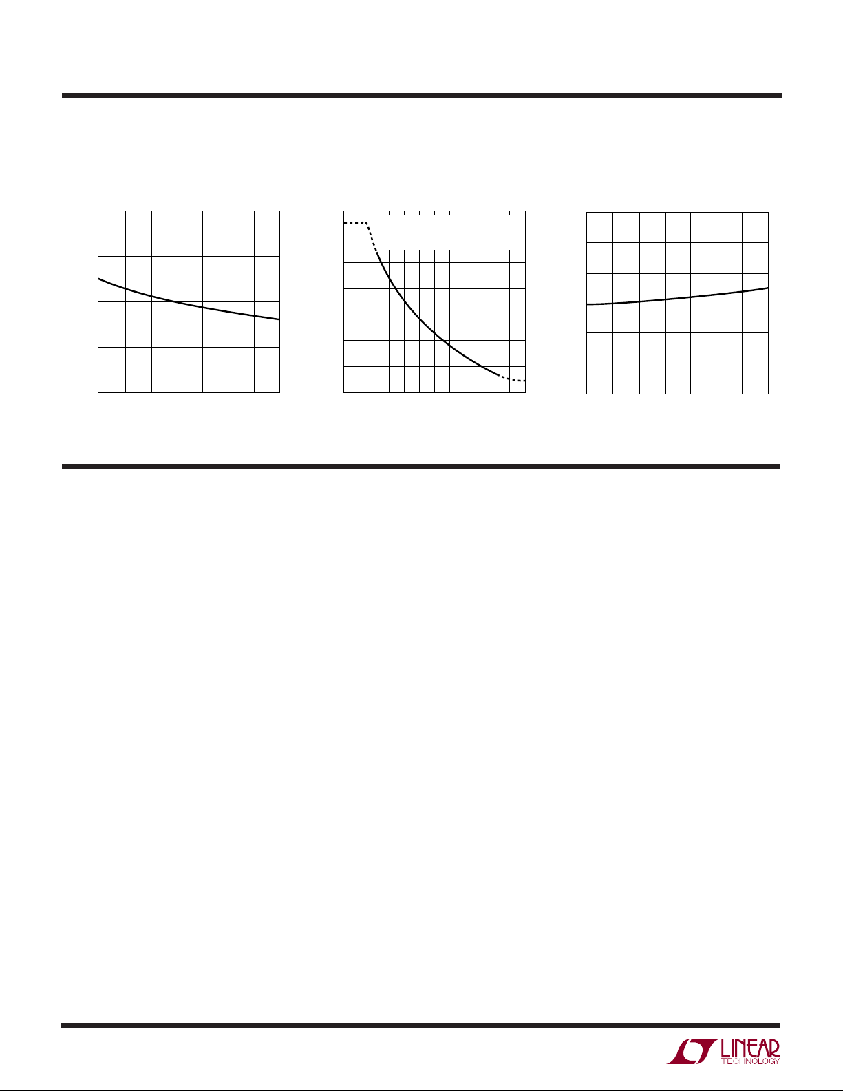
Voltage
SEC
94% Efficient 3.3V, 20A Synchronous Forward
Converter
The synchronous forward converter in Figure 11 is based
on the LT1950 and uses MOSFETs as synchronous output
rectifiers to provide an efficient 3.3V, 20A isolated output
from 48V input. The output rectifiers are driven by the
LTC1698 which also serves as an error amplifier and
optocoupler driver. Efficiency and transient response
are shown in Figures 9 and 10. Peak efficiencies of 94%
and ultra-fast transient response are superior to presently
available power modules. In addition, the circuit in Figure 11
is an all-ceramic capacitor solution providing low output
ripple voltage and improved reliability. The LT1950-based
converter can be used to replace power module converters
at a much lower cost. The LT1950 solution benefits from
thermal conduction of the system board resulting in
higher efficiencies and lower rise in component temperatures. The 7mm height allows dense packaging and the
circuit can be easily adjusted to provide an output voltage
from 1.23V to 15V. In addition, higher currents are achievable by simple scaling of power components. The LT1950based solution in Figure 11 is a powerful topology for
replacement of a wide range of power modules.
100
95
90
85
EFFICIENCY (%)
80
75
70
0
Figure 9. LT1950-Based Synchronous Forward
Converter Efficiency vs Load Current
5101520
LOAD CURRENT (A)
VIN = 48V
= 3.3V
V
OUT
= 235kHz
f
OSC
1950 F09
LT1950
V
OUT
(100mV/DIV)
POWER
MODULE
V
OUT
(100mV/DIV)
500µs/DIV
Figure 10. Output Voltage Transient Response
to Load Steps (0A to 3.3A) LT1950 (Trace1)
vs Power Module (Trace 2)
1950 F10
1950fa
15
Page 16

LT1950
WUUU
APPLICATIO S I FOR ATIO
10V
R6
18k
C3
10nF
R3
4.7k
0.1µF
BIAS
C
1µF
U1
6
5
4
IN
R18
27k
D3
R1
4.7k
R17, 210k
C1
0.1µF
R4, 18k
R9
470k
10V
COMP
+V
1
2
3
4
5
6
7
8
IN
BIAS
100k
UV
COMP
FB
R
OSC
SYNC
SLOPE
V
REF
SHDN
GND
LT1950
BOOST
I
BLANK
Q4
BC847BF
4.7µF
V
SEC
V
PGND
GATE
V
IN2
SENSE
R2
4.7k
C6
IN
100k
470k
16
15
14
13
12
11
10
9
R5
UV
+V
C
S
BAT760
R7
255Ω
D1
BAS516
C4
1000pF
U4
HCPL-M453
36V
TO 72V
INPUT
10V
1
10V
3
BIAS
U2A
8
LTC1693-1
2
BAT760
BIAS
U2B
6
LTC1693-1
4
+V
–V
1
2
3
IN
IN
7
D2
5
220pF
2.2µF
100V
X5R
47Ω
T2
C
IN
T1
STG-0313W
1µF
X5R
C9, 33nF
+V
Q2
Si7380
2×
7V
BIAS
R13
270Ω
R14
1.2k
01
R15
4.7k
CG
1
2
3
4
5
6
7
8
R16
2.8k
CG
V
DD
CG
PGND
GND
OPTO
V
COMP
MARG
V
FB
LTC1698
=1.233V
Q1
FG
Si4490
R
S
0.015Ω
C
S
SYNC
560Ω
L1
C.PI-1365-1R2
Q3
Si7380
2×
16
FG
15
SYNC
14
V
AUX
13
I
COMP
12
+I
SNS
11
–I
SNS
10
PWTOK
9
OVP
FG
SYNC
+V
3.3V
20A
C
01
100µF
X5R
4×
0.1µF
01
COMP
Figure 11. 36V to 72V Input to 3.3V at 20A Synchronous Forward Converter
16
1950fa
Page 17

WUUU
APPLICATIO S I FOR ATIO
LT1950
High Efficiency, Isolated 26V 5A Output,
Nonsynchronous Forward Converter
Figure 13 illustrates a nonsynchronous forward converter
based on the LT1950 to provide a highly efficient, 26V 5A
isolated output from 48V input. The LT1950-based converter using a single switch topology and utilizing the
LT1950s adaptive maximum duty cycle clamp is a simple
and highly optimized solution. Peak efficiencies of 92.8%
(Figure 12) are achievable. Transformer and inductor are
standard components. The quarter brick sized DC/DC
converter (2.3" by 1.45") delivers over 125W and is only
0.4" high. The 26V converter can be used as a “front line”
(isolating) converter in telecom systems with multiple
outputs.
+V
IN
C
36V
TO 72V
INPUT
–V
IN
2.2µF
100V
X5R
IN
T1
PA0581
MBR20200CT
94
93
92
91
90
89
88
EFFICIENCY (%)
87
86
85
84
1
2
LOAD CURRENT (A)
VIN = 48V
V
OUT
f
OSC
3
4
Figure 12. LT1950-Based Nonsynchronous
Forward Converter Efficiency vs Load
Current (Figure 13 Circuit)
+V
47µH
OUT
= 26V
= 235kHz
5
1950 F12
232k
24.9k
18k
–
4
5
1
U3
LT1797
47k
3
+
2
1µF
U2
LT1009
FMMT625
1µF
6.8k
0.1µF
210k
27k
5
6
3
9
4
2
1
SLOPE
V
REF
R
OSC
BLANK
SYNC
FB
COMP
LT1950
V
SHDN
GATE
I
SENSE
PGND
V
SEC
GND
10V
+V
BIAS
IN
15
V
IN
11
IN2
470k
16
7
18k
12
10
8
13
Si7450
0.015
47µF
470pF
330R
OC1
Figure 13. 36V to 72V Input to 26V at 5A Nonsynchronous Forward Converter
22k
8.2V
1950 F13
1950fa
17
Page 18

LT1950
WUUU
APPLICATIO S I FOR ATIO
10.5k
1.21k
BOOST
PGND
I
SENSE
BLANK
V
IN
V
SEC
V
GATE
V
IN
IN2
3.3V BIAS
16
15
14
13
12
11
10
9
47k
C3
4.7µF
16V
L1
4.7µH
D2
BAS516
R9, 47Ω
C6
0.01µF
R8
*L2, L3 (COUPLED INDUCTORS)
VP5-0155
+V
OUT
C1
R3
2200pF
R1
R2
R4
133k
35.7k
18k
R5
16.2k
C2
0.1µF
R6
1
2
3
4
5
6
7
8
COMP
FB
R
OSC
SYNC
SLOPE
V
REF
SHDN
GND
R7
71.5k
LT1950
Figure 14. 4V to 36V Input, 12V/1.5A Automotive SEPIC Converter
C
IN
10µF
50V
TDK
L2*
C4
4.7µF
16V
V
4V TO 36V
C5
10µF
50V
Q1
Si7456
R10
0.010Ω
IN
MBRD660CT
L3*
D1
+V
OUT
12V, 1.5A
C
OUT
47µF, 16V
X5R, TDK
×4
18
1950fa
Page 19

PACKAGE DESCRIPTIO
LT1950
U
GN Package
16-Lead Plastic SSOP (Narrow .150 Inch)
(Reference LTC DWG # 05-08-1641)
.045 ±.005
.254 MIN
RECOMMENDED SOLDER PAD LAYOUT
.007 – .0098
(0.178 – 0.249)
.016 – .050
NOTE:
1. CONTROLLING DIMENSION: INCHES
2. DIMENSIONS ARE IN
3. DRAWING NOT TO SCALE
*DIMENSION DOES NOT INCLUDE MOLD FLASH. MOLD FLASH
SHALL NOT EXCEED 0.006" (0.152mm) PER SIDE
**DIMENSION DOES NOT INCLUDE INTERLEAD FLASH. INTERLEAD
FLASH SHALL NOT EXCEED 0.010" (0.254mm) PER SIDE
(0.406 – 1.270)
INCHES
(MILLIMETERS)
.150 – .165
.0250 TYP.0165 ± .0015
.015 ± .004
(0.38 ± 0.10)
0° – 8° TYP
× 45°
.229 – .244
(5.817 – 6.198)
.053 – .068
(1.351 – 1.727)
.008 – .012
(0.203 – 0.305)
16
15
12
.189 – .196*
(4.801 – 4.978)
14
12 11 10
13
5
4
3
678
.0250
(0.635)
BSC
.009
(0.229)
9
.004 – .0098
(0.102 – 0.249)
REF
.150 – .157**
(3.810 – 3.988)
GN16 (SSOP) 0502
Information furnished by Linear Technology Corporation is believed to be accurate and reliable.
However, no responsibility is assumed for its use. Linear Technology Corporation makes no representation that the interconnection of its circuits as described herein will not infringe on existing patent rights.
1950fa
19
Page 20

LT1950
RELATED PARTS
PART NUMBER DESCRIPTION COMMENTS
LT1534 Ultralow Noise 2A Switching Regulator Reduces Conducted and Radiated EMI, Low Switching Harmonics,
20kHz to 250kHz Switching Frequency
LT1619 Low Voltage Current Mode Controller 1.9V ≤ VIN ≤ 18V, 300kHz Operation, Boost, Flyback, SEPIC
LT1681/LT3781 Dual Transistor Synchronous Forward Controller Operation Up to 72V Maximum
LTC1693 High Speed MOSFET Driver 1.5A Peak Output Current, 16ns Rise/Fall Time at VCC = 12V, CL = 1nF
LTC1698 Secondary Synchronous Rectifier Controller Use with the LT1950 or LT1681, Isolated Power Supplies,
Contains Voltage Margining, Optocoupler Driver, Synchronization
Circuit with the Primary Side
LT1725 General Purpose Isolated Flyback Controller No Optoisolator Required, Accurate Regulation Without User Trims,
50kHz to 250kHz Switching Frequency, SSOP-16 Package
LTC1871 Wide Input Range, No R
LT1910 Protected High Side MOSFET Driver 8V to 48V Supply Range, Protected –15V to 60V Supply Transient
LTC3440 Micropower Buck-Boost DC/DC Converter Synchronous, Single Inductor, No Schottky Diode Required
LTC3704 Positive-to-Negative DC/DC Controller 2.5V ≤ VIN ≤ 36V, No R
No R
is a trademark of Linear Technology Corporation.
SENSE
TM
Controller Operation as Low as 2.5V Input, Boost, Flyback, SEPIC
SENSE
Current Mode Operation,
Excellent Transient Response
SENSE
20
Linear Technology Corporation
1630 McCarthy Blvd., Milpitas, CA 95035-7417
(408) 432-1900 ● FAX: (408) 434-0507 ● www.linear.com
1950fa
LT/TP 0504 1K REV A • PRINTED IN USA
© LINEAR TECHNOLOGY CORPORATION 2003
 Loading...