

Page 1
FEATURES
Final Electrical Specifications
FREQUENCY (Hz)
10k 100k 1M 10M 100M
GAIN (dB)
1809 TA01a
10
0
–10
–20
–30
–40
–50
–60
–70
–80
–90
VS = 3V, 0V
V
IN
= 2.5V
P-P
LT1809
180MHz, 350V/µs
Rail-to-Rail Input and Output
Low Distortion Op Amp
January 2000
U
DESCRIPTIO
■
–3dB Bandwidth: 320MHz, AV = 1
■
Gain-Bandwidth Product: 180MHz, AV ≥ 10
■
Slew Rate: 350V/µs
■
Wide Supply Range: 2.5V to 12.6V
■
Large Output Current: 85mA
■
Low Distortion, 5MHz: –90dBc
■
Input Common Mode Range Includes Both Rails
■
Output Swings Rail-to-Rail
■
Input Offset Voltage, Rail-to-Rail: 2.5mV Max
■
Common Mode Rejection: 89dB Typ
■
Power Supply Rejection: 87dB Typ
■
Open-Loop Gain: 100V/mV Typ
■
Shutdown Pin
■
8-Pin SO-8 Package
■
Operating Temperature Range –40°C to 85°C
U
APPLICATIO S
■
Active Filters
■
Rail-to-Rail Buffer Amplifiers
■
Driving A/D Converters
■
Low Voltage Signal Processing
■
Video Line Driver
The LT®1809 is a low distortion rail-to-rail input and
output op amp with a 350V/µs slew rate. The amplifier has
a –3dB bandwidth of 320MHz at unity-gain, a gain-bandwidth product of 180MHz (AV ≥ 10) and an 85mA output
current to fit the needs of low voltage, high performance
signal conditioning systems.
The LT1809 has an input range that includes both supply
rails and an output that swings within 20mV of either
supply rail to maximize the signal dynamic range in low
supply applications.
The LT1809 has very low distortion (–90dBc) up to 5MHz
that allows it to be used in high performance data acquisition systems.
The LT1809 maintains its performance for supplies from
2.5V to 12.6V and is specified at 3V, 5V and ±5V supplies.
The inputs can be driven beyond the supplies without
damage or phase reversal of the output.
The LT1809 is available in the 8-pin SO package with the
standard op amp pinout. This device can be used as a plugin replacement for many op amps to improve input/output
range and performance.
, LTC and LT are registered trademarks of Linear Technology Corporation.
TYPICAL APPLICATIO
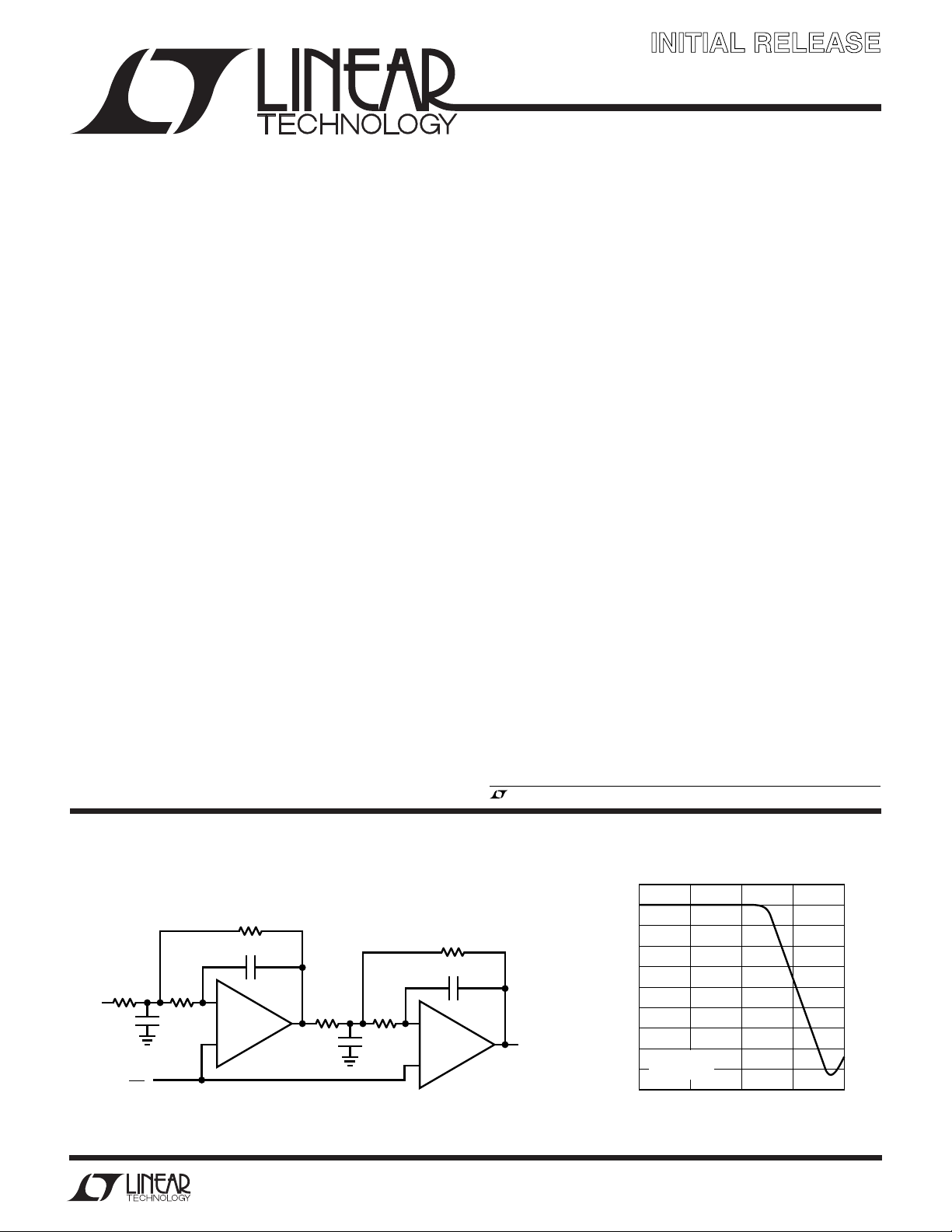
Single 3V Supply, 4MHz, 4th Order Butterworth Filter
V
232Ω
IN
665Ω
220pF
–
+
V
S
2
232Ω
47pF
LT1809
U
Filter Frequency Response
274Ω
22pF
274Ω
Information furnished by Linear Technology Corporation is believed to be accurate and reliable.
However, no responsibility is assumed for its use. Linear Technology Corporation makes no representation that the interconnection of its circuits as described herein will not infringe on existing patent rights.
562Ω
470pF
–
LT1809
+
V
OUT
1809 TA01
1
Page 2

LT1809
WW
W
ABSOLUTE AXI U RATI GS
U
UUW
PACKAGE/ORDER I FOR ATIO
(Note 1)
Total Supply Voltage (V+ to V–) ........................... 12.6V
Input Voltage (Note 2) ..............................................±V
Input Current (Note 2) ........................................ ±10mA
Output Short-Circuit Duration (Note 3)............ Indefinite
Operating Temperature Range (Note 4) .. –40°C to 85°C
Specified Temperature Range (Note 5)... –40°C to 85°C
Junction Temperature...........................................150°C
Storage Temperature Range ................. –65°C to 150°C
Lead Temperature (Soldering, 10 sec)..................300°C
TOP VIEW
SHDN
S
1
–IN
2
+IN
3
–
V
4
S8 PACKAGE
8-LEAD PLASTIC SO
T
= 150°C, θJA = 190°C/W
JMAX
8
NC
+
V
7
OUT
6
NC
5
ORDER PART
NUMBER
LT1809CS8
LT1809IS8
S8 PART
MARKING
1809
1809I
Consult factory for Military grade parts.
ELECTRICAL CHARACTERISTICS
TA = 25°C. VS = 5V, 0V; VS = 3V, 0V; V
SYMBOL PARAMETER CONDITIONS MIN TYP MAX UNITS
V
OS
∆V
I
B
∆I
B
I
OS
∆I
OS
e
n
i
n
C
IN
A
VOL
CMRR Common Mode Rejection Ratio VS = 5V, V
PSRR Power Supply Rejection Ratio VS = 2.5V to 10V, V
Input Offset Voltage VCM = V
Input Offset Shift VCM = V– to V
OS
Input Bias Current VCM = V
Input Bias Current Shift VCM = V– to V
Input Offset Current VCM = V
Input Offset Current Shift VCM = V– to V
Input Noise Voltage Density f = 10kHz 16 nV/√Hz
Input Noise Current Density f = 10kHz 5 pA/√Hz
Input Capacitance 2pF
Large-Signal Voltage Gain VS = 5V, VO = 0.5V to 4.5V, RL = 1k 35 90 V/mV
Input Common Mode Range V
Minimum Supply Voltage (Note 6) 2.3 2.5 V
= open; VCM = V
SHDN
= half supply unless otherwise noted.
OUT
+
–
= V
V
CM
= V
V
CM
V
= V
CM
V
= 5V, VO = 1V to 4V, RL = 100Ω 4.5 10 V/mV
S
= 3V, VO = 0.5V to 2.5V, RL = 1k 22 42 V/mV
V
S
= 3V, V
V
S
+
–
+
–
= V– to V
CM
= V– to V
CM
+
–27.5 –13 µA
+
+
+
+
= 0V 73 87 dB
CM
69 82 dB
64 78 dB
0.6 2.5 mV
0.6 2.5 mV
0.3 1.75 mV
1.8 8 µA
11.8 35.5 µA
0.05 1.2 µA
0.2 4 µA
0.25 5.2 µA
–
+
V
V
2
Page 3
LT1809
ELECTRICAL CHARACTERISTICS
TA = 25°C. VS = 5V, 0V; VS = 3V, 0V; V
SYMBOL PARAMETER CONDITIONS MIN TYP MAX UNITS
V
OL
V
OH
I
SC
I
S
GBW Gain-Bandwidth Product Frequency = 2MHz 160 MHz
SR Slew Rate VS = 5V, AV = –1, RL = 1k, VO = 4V
THD Total Harmonic Distortion VS = 5V, AV = 1, RL = 1k, VO = 2V
t
S
∆G Differential Gain (NTSC) VS = 5V, AV = 2, RL = 150Ω 0.015 %
∆θ Differential Phase (NTSC) 0.05 %
Output Voltage Swing LOW (Note 7) No Load 6 20 mV
Output Voltage Swing HIGH (Note 7) No Load 17 40 mV
Short-Circuit Current VS = 5V ±50 ±85 mA
Supply Current 12.5 17 mA
Disable Supply Current VS = 5V, V
Settling Time 0.01%, VS = 5V, V
= open; VCM = V
SHDN
= half supply unless otherwise noted.
OUT
I
= 5mA 40 80 mV
SINK
= 25mA 150 300 mV
I
SINK
= 5mA 80 160 mV
I
SOURCE
I
= 25mA 300 500 mV
SOURCE
= 3V ±40 ±70 mA
V
S
= 0V 0.55 0.8 mA
SHDN
= 3V, V
V
S
= 0V 0.31 0.5 mA
SHDN
P-P
, fC = 5MHz –86 dB
P-P
= 2V, AV = 1, RL = 1k 40 ns
STEP
300 V/µs
The ● denotes the specifications which apply over the 0°C ≤ TA ≤ 70°C temperature range. VS = 5V, 0V; VS = 3V, 0V; V
VCM = V
= half supply unless otherwise noted.
OUT
SHDN
= open;
SYMBOL PARAMETER CONDITIONS MIN TYP MAX UNITS
V
OS
Input Offset Voltage VCM = V
VOS TC Input Offset Voltage Drift (Note 8) VCM = V
∆V
I
∆I
I
∆I
A
B
B
OS
OS
VOL
Input Offset Voltage Shift VCM = V
OS
Input Bias Current VCM = V+ – 0.1V ● 210 µA
Input Bias Current Shift VCM = V
Input Offset Current VCM = V+ – 0.1V ● 0.05 1.5 µA
Input Offset Current Shift VCM = V
Large-Signal Voltage Gain VS = 5V, VO = 0.5V to 4.5V, RL = 1k ● 25 80 V/mV
CMRR Common Mode Rejection Ratio VS = 5V, VCM = V
Input Common Mode Range ● V
PSRR Power Supply Rejection Ratio VS = 2.5V to 10V, V
+
–
= V
V
CM
+
–
V
= V
CM
–
+
to V
–
V
= V
+ 0.2V ● –30 –14 µA
CM
–
+ 0.2V to V+ – 0.1V ● 12 40 µA
–
= V
V
V
V
V
+ 0.2V ● 0.40 4.5 µA
CM
–
+ 0.2V to V+ – 0.1V ● 0.45 6 µA
= 5V, VO = 1V to 4V, RL = 100Ω ● 3.5 8.5 V/mV
S
= 3V, VO = 0.5V to 2.5V, RL = 1k ● 16 40 V/mV
S
= 3V, VCM = V
S
–
+
to V
–
+
to V
= 0V ● 71 83 dB
CM
● 13 mV
● 13 mV
● 925µV/°C
● 925µV/°C
● 0.5 2 mV
● 67.5 80 dB
● 63.5 75 dB
–
+
V
Minimum Supply Voltage (Note 6) ● 2.3 2.5 V
V
OL
Output Voltage Swing LOW (Note 7) No Load ● 825 mV
I
= 5mA ● 40 80 mV
SINK
= 25mA ● 160 320 mV
I
SINK
V
3
Page 4

LT1809
ELECTRICAL CHARACTERISTICS
The ● denotes the specifications which apply over the 0°C ≤ TA ≤ 70°C temperature range. VS = 5V, 0V; VS = 3V, 0V; V
VCM = V
SYMBOL PARAMETER CONDITIONS MIN TYP MAX UNITS
V
OH
I
SC
I
S
GBW Gain-Bandwidth Product ● 145 MHz
SR Slew Rate VS = 5V, AV = –1, RL = 1k, VO = 4V
= half supply unless otherwise noted.
OUT
Output Voltage Swing HIGH (Note 7) No Load ● 50 100 mV
= 5mA ● 110 220 mV
I
SOURCE
= 25mA ● 340 600 mV
I
SOURCE
Short-Circuit Current VS = 5V ● ±45 ±75 mA
V
= 3V ● ±35 ±65 mA
S
Supply Current ● 15 20 mA
Disable Supply Current VS = 5V, V
= 3V, V
V
S
= 0V ● 0.58 1 mA
SHDN
= 0V ● 0.35 0.75 mA
SHDN
P-P
● 250 V/µs
SHDN
= open;
The ● denotes the specifications which apply over the –40°C ≤ TA ≤ 85°C temperature range. VS = 5V, 0V; VS = 3V, 0V; V
VCM = V
= half supply unless otherwise noted. (Note 5)
OUT
SHDN
= open;
SYMBOL PARAMETER CONDITIONS MIN TYP MAX UNITS
Vos Input Offset Voltage VCM = V
Vos TC Input Offset Voltage Drift (Note 8) VCM = V
∆Vos Input Offset Voltage Shift VCM = V
I
B
∆I
B
I
OS
∆I
OS
A
VOL
Input Bias Current VCM = V+ – 0.1V ● 212 µA
Input Bias Current Shift VCM = V– + 0.2V to V+ – 0.1V ● 14 47 µA
Input Offset Current VCM = V+ – 0.1V ● 0.08 2 µA
Input Offset Current Shift VCM = V– + 0.2V to V+ – 0.1V ● 0.58 7.5 µA
Large-Signal Voltage Gain VS = 5V, VO = 0.5V to 4.5V, RL = 1k ● 20 60 V/mV
CMRR Common Mode Rejection Ratio VS = 5V, VCM = V– to V
Input Common Mode Range ● V
+
–
= V
V
CM
+
–
V
= V
CM
–
= V– + 0.2V ● –35 –17 µA
V
CM
= V– + 0.2V ● 0.5 6 µA
V
CM
= 5V, VO = 1V to 4V, RL = 100Ω ● 2.5 7 V/mV
V
S
V
= 3V, VO = 0.5V to 2.5V, RL = 1k ● 12 35 V/mV
S
V
= 3V, VCM = V– to V
S
+
+
● 1 3.5 mV
● 1 3.5 mV
● 925µV/°C
● 925µV/°C
● 0.5 2.25 mV
● 66.5 80 dB
● 62.5 75.5 dB
–
+
V
PSRR Power Supply Rejection Ratio VS = 2.5V to 10V, VCM = 0V ● 71 83.5 dB
Minimum Supply Voltage (Note 6) ● 2.3 2.5 V
V
OL
V
OH
I
SC
I
S
Output Voltage Swing LOW (Note 7) No Load ● 830 mV
I
= 5mA ● 45 90 mV
SINK
= 25mA ● 170 340 mV
I
SINK
Output Voltage Swing HIGH (Note 7) No Load ● 55 120 mV
= 5mA ● 110 230 mV
I
SOURCE
I
= 25mA ● 350 620 mV
SOURCE
Short-Circuit Current VS = 5V ● ±35 ±70 mA
= 3V ● ±30 ±60 mA
V
S
Supply Current ● 15 21 mA
Disable Supply Current VS = 5V, V
= 3V, V
V
S
= 0V ● 0.58 1.1 mA
SHDN
= 0V ● 0.35 0.85 mA
SHDN
V
4
Page 5

LT1809
ELECTRICAL CHARACTERISTICS
The ● denotes the specifications which apply over the –40°C ≤ TA ≤ 85°C temperature range. VS = 5V, 0V; VS = 3V, 0V; V
VCM = V
SYMBOL PARAMETER CONDITIONS MIN TYP MAX UNITS
GBW Gain-Bandwidth Product Frequency = 2MHz ● 140 MHz
SR Slew Rate VS = 5V, AV = -1, RL = 1k, VO = 4V
= half supply unless otherwise noted. (Note 5)
OUT
P-P
● 180 V/µs
SHDN
= open;
TA = 25°C. VS = ±5V, V
= open, VCM = 0V, V
SHDN
= 0V unless otherwise noted.
OUT
SYMBOL PARAMETER CONDITIONS MIN TYP MAX UNITS
V
OS
Input Offset Voltage VCM = V
∆Vos Input Offset Voltage Shift VCM = V– to V
I
B
∆I
B
I
OS
∆I
OS
e
n
i
n
C
in
A
VOL
Input Bias Current VCM = V
Input Bias Current Shift VCM = V– to V
Input Offset Current VCM = V
Input Offset Current Shift VCM = V– to V
Input Noise Voltage Density f = 10kHz 16 nV/√Hz
Input Noise Current Density f = 10kHz 5 pA/√Hz
Input Capacitance f = 100kHz 2 pF
Large-Signal Voltage Gain VO = –4V to 4V, RL = 1k 45 100 V/mV
CMRR Common Mode Rejection Ratio V
Input Common Mode Range V
PSRR Power Supply Rejection Ratio V
V
OL
V
OH
I
SC
I
S
Output Voltage Swing LOW (Note 7) No Load 8 30 mV
Output Voltage Swing HIGH (Note 7) No Load 30 60 mV
Short-Circuit Current ±60 ±85 mA
Supply Current 15 20 mA
Disable Supply Current V
+
–
V
= V
CM
= V
V
CM
= V
V
CM
= –2.5V to 2.5V, RL = 100Ω 512 V/mV
V
O
= V– to V
CM
+
= 2.5V to 10V, V– = 0V 73 87 dB
= 5mA 46 100 mV
I
SINK
= 25mA 170 350 mV
I
SINK
I
SOURCE
I
SOURCE
SHDN
+
+
–
+
+
–
+
+
–30 –12.5 µA
73 89 dB
= 5mA 90 200 mV
= 25mA 310 600 mV
= 0V 0.6 0.9 mA
0.8 3 mV
0.8 3 mV
0.35 2 mV
210 µA
13.5 42.5 µA
0.05 2 µA
0.4 5 µA
0.45 7 µA
–
+
V
GBW Gain-Bandwidth Product Frequency = 2MHz 120 180 MHz
SR Slew Rate AV = –1, RL = 1k, VO = ±4V, 175 350 V/µs
Measure at V
HD Total Harmonic Distortion AV = 1, RL = 1k, VO = 2V
t
S
Settling Time 0.01%, V
= ±3V
O
, fC = 5MHz –90 dB
P-P
= 5V, AV = 1, RL = 1k 60 nS
STEP
∆G Differential Gain (NTSC) AV = 2, RL = 150 0.01 %
∆θ Differential Phase (NTSC) 0.01 %
V
5
Page 6

LT1809
ELECTRICAL CHARACTERISTICS
The ● denotes the specifications which apply over the 0°C ≤ TA ≤ 70°C temperature range. VS = ±5V, V
V
= 0V unless otherwise noted.
OUT
SYMBOL PARAMETER CONDITIONS MIN TYP MAX UNITS
V
OS
Input Offset Voltage VCM = V
VOS TC Input Offset Voltage Drift (Note 8) VCM = V
∆V
I
∆I
I
∆I
A
B
B
OS
OS
VOL
Input Offset Voltage Shift VCM = V– to V
OS
Input Bias Current VCM = V+ – 0.1V ● 2.5 12.5 µA
Input Bias Current Shift VCM = V– + 0.2V to V+ – 0.1V ● 14 50 µA
Input Offset Current VCM = V+ – 0.1V ● 0.06 2.25 µA
Input Offset Current Shift VCM = V– + 0.2V to V+ – 0.1V ● 0.56 8.25 µA
Large-Signal Voltage Gain VO = –4V to 4V, RL = 1k ● 35 90 V/mV
CMRR Common Mode Rejection Ratio V
Input Common Mode Range ● V
PSRR Power Supply Rejection Ratio V
V
OL
V
OH
I
SC
I
S
Output Voltage Swing LOW (Note 7) No Load ● 10 40 mV
Output Voltage Swing HIGH (Note 7) No Load ● 60 120 mV
Short-Circuit Current ● ±50 ±75 mA
Supply Current ● 17.5 25 mA
Disable Supply Current V
GBW Gain-Bandwidth Product Frequency = 2MHz ● 100 170 MHz
SR Slew Rate AV = –1, RL = 1k, VO = ±4V, ● 150 300 V/µs
+
–
= V
V
CM
+
–
= V
V
CM
= V– +0.2V ● –37.5 –15 µA
V
CM
V
= V– + 0.2V ● 0.5 6 µA
CM
V
= –2.5V to 2.5V, RL = 100Ω ● 410 V/mV
O
= V– to V
CM
+
= 2.5V to 10V, V– = 0V ● 71 83 dB
I
= 5mA ● 45 100 mV
SINK
= 25mA ● 185 370 mV
I
SINK
I
SOURCE
I
SOURCE
SHDN
Measure at V
+
+
= 5mA ● 110 220 mV
= 25mA ● 360 625 mV
= 0V ● 0.6 1.1 mA
= ±3V
O
● 1 3.25 mV
● 1 3.25 mV
● 10 25 µV/°C
● 10 25 µV/°C
● 0.5 2.15 mV
● 73.5 86 dB
= open, VCM = 0V,
SHDN
–
+
V
V
The ● denotes the specifications which apply over the –40°C ≤ TA ≤ 85°C temperature range. VS = ±5V, V
V
= 0V unless otherwise noted. (Note 5)
OUT
= open, VCM = 0V,
SHDN
SYMBOL PARAMETER CONDITIONS MIN TYP MAX UNITS
V
OS
Input Offset Voltage VCM = V
VOS TC Input Offset Voltage Drift (Note 8) VCM = V
∆V
I
∆I
B
B
Input Offset Voltage Shift VCM = V– to V
OS
Input Bias Current VCM = V+ – 0.1V ● 2.8 14 µA
Input Bias Current Shift VCM = V– + 0.2V to V+ – 0.1V ● 19.8 59 µA
+
–
= V
V
CM
+
–
V
= V
CM
V
= V– + 0.2V ● –45 –17 µA
CM
+
● 1 3.75 mV
● 1 3.75 mV
● 10 25 µV/°C
● 10 25 µV/°C
● 0.5 2.5 mV
6
Page 7

LT1809
ELECTRICAL CHARACTERISTICS
The ● denotes the specifications which apply over the –40°C ≤ TA ≤ 85°C temperature range. VS = ±5V, V
V
= 0V unless otherwise noted. (Note 3)
OUT
SYMBOL PARAMETER CONDITIONS MIN TYP MAX UNITS
I
OS
∆I
OS
A
VOL
CMRR Common Mode Rejection Ratio V
PSRR Power Supply Rejection Ratio V
V
OL
V
OH
I
SC
I
S
GBW Gain-Bandwidth Product Frequency = 2MHz ● 90 160 MHz
SR Slew Rate AV = –1, RL = 1k, VO = ±4V, ● 110 220 V/µs
Note 1: Absolute Maximum Ratings are those values beyond which the life
of a device may be impaired.
Note 2: The inputs are protected by back-to-back diodes. If the differential
input voltage exceeds 1.4V, the input current should be limited to less than
10mA.
Note 3: A heat sink may be required to keep the junction temperature
below the absolute maximum rating when the output is shorted
indefinitely.
Note 4: The LT1809C/LT1809I are guaranteed functional over the
operating temperature range of –40
Input Offset Current VCM = V+ – 0.1V ● 0.08 2.5 µA
= V– + 0.2V ● 0.6 8 µA
V
CM
Input Offset Current Shift VCM = V– + 0.2V to V+ – 0.1V ● 0.68 10.5 µA
Large-Signal Voltage Gain VO = –4V to 4V, RL = 1k ● 25 80 V/mV
= –2.5V to 2.5V, RL = 100Ω ● 310 V/mV
V
O
= V– to V
CM
+
● 72 86 dB
Input Common Mode Range ● V
+
= 2.5V to 10V, V– = 0V ● 71 83.5 dB
Output Voltage Swing LOW (Note 7) No Load ● 10 45 mV
= 5mA ● 50 100 mV
I
SINK
I
= 25mA ● 200 400 mV
SINK
Output Voltage Swing HIGH (Note 7) No Load ● 70 140 mV
= 5mA ● 115 240 mV
I
SOURCE
= 25mA ● 360 650 mV
I
SOURCE
Short-Circuit Current ● ±40 ±75 mA
Supply Current ● 19 25 mA
Disable Supply Current V
= 0V ● 0.65 1.15 mA
SHDN
Measure at V
= ±2V
O
Note 5: The LT1809C is guaranteed to meet specified performance from
0°C to 70°C. The LT1809C is designed, characterized and expected to
meet specified performance from –40°C to 85°C but is not tested or QA
sampled at these temperatures. The LT1809I is guaranteed to meet
specified performance from –40°C to 85°C.
Note 6: Minimum supply voltage is guaranteed by power supply rejection
ratio test.
Note 7: Output voltage swings are measured between the output and
power supply rails.
o
C and 85oC.
Note 8: This parameter is not 100% tested.
= open, VCM = 0V,
SHDN
–
+
V
V
PACKAGE DESCRIPTIO
0.010 – 0.020
(0.254 – 0.508)
0.008 – 0.010
(0.203 – 0.254)
*
DIMENSION DOES NOT INCLUDE MOLD FLASH. MOLD FLASH
SHALL NOT EXCEED 0.006" (0.152mm) PER SIDE
**
DIMENSION DOES NOT INCLUDE INTERLEAD FLASH. INTERLEAD
FLASH SHALL NOT EXCEED 0.010" (0.254mm) PER SIDE
× 45°
0.016 – 0.050
(0.406 – 1.270)
0°– 8° TYP
U
Dimensions in inches (millimeters) unless otherwise noted.
S8 Package
8-Lead Plastic Small Outline (Narrow 0.150)
(LTC DWG # 05-08-1610)
0.189 – 0.197*
(4.801 – 5.004)
7
0.053 – 0.069
(1.346 – 1.752)
0.014 – 0.019
(0.355 – 0.483)
TYP
0.004 – 0.010
(0.101 – 0.254)
0.050
(1.270)
BSC
0.228 – 0.244
(5.791 – 6.197)
8
1
2
6
3
5
0.150 – 0.157**
(3.810 – 3.988)
4
SO8 1298
7
Page 8

LT1809
TYPICAL APPLICATIO
U
Single Supply Video Line Driver
The LT1809 is a wideband rail-to-rail op amp with high
output current that allows it to drive video signals in low
supply applications. Figure 1 depicts a single supply video
line driver with AC coupling to minimize the quiescent
power dissipation. Resistors R1 and R2 are used to levelshift the input and output to provide the largest signal
swing. The gain of two is set up with R3 and R4 to restore
the signal at V
which is attenuated by 6dB due to the
OUT
C1
33µF
V
IN
R
T
75Ω
R1
5k
+
R2
5k
3
+
LT1809
2
–
R3
1k
+
C2
150µF
5V
7
6
4
R4
1k
matching of the 75Ω line with the back-terminated resistor, R5. The back termination will eliminate any reflection
of the signal that comes from the load. The input termination resistor, RT, is optional—it is used only if matching of
the incoming line is necessary. The values of C1, C2 and
C3 are selected to minimize the droop of the luminance
signal. In some less stringent requirements, the value of
capacitors could be reduced.
C3
1000µF
+
R5
75Ω
75Ω
COAX CABLE
R
LOAD
75Ω
V
1809 TA02
OUT
Figure 1. Single Supply Video Line Driver
RELATED PARTS
PART NUMBER DESCRIPTION COMMENTS
LT1632/LT1633 Dual/Quad 45MHz, 45V/µs Rail-to-Rail Input and Output Op Amps High DC Accuracy, 1.35mV V
Max Supply Current 5.2mA per Amplifier
LT1630/LT1631 Dual/Quad 30MHz, 10V/µs Rail-to-Rail Input and Output Op Amps High DC Accuracy, 525µV V
Max Supply Current 4.4mA per Amplifier
LT1215/LT1216 Dual/Quad 23MHz, 50V/µs Single Supply Precision Op Amps Input Common Mode Includes Ground, 450µV V
6µV/°C Max Drift, Max Supply Current 6.6mA per Amplifier
OS(MAX)
, 70mA Output Current,
OS(MAX)
, 70mA Output Current,
OS(MAX)
,
8
Linear Technology Corporation
1630 McCarthy Blvd., Milpitas, CA 95035-7417
(408) 432-1900 ● FAX: (408) 434-0507 ● www.linear-tech.com
1809i LT/TP 0100 4K • PRINTED IN USA
LINEAR TECHNOLOGY CORPORATION 2000
 Loading...