

Page 1
LT1946A
LOAD CURRENT (mA)
0
100 200 300 400 500
EFFICIENCY (%)
1946A TA01
90
85
80
75
70
65
60
55
50
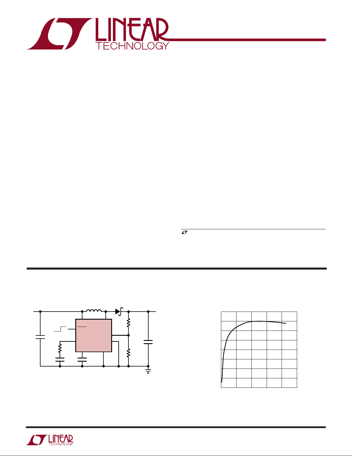
2.7MHz Boost DC/DC
Converter with 1.5A Switch
and Soft-Start
FEATURES
■
1.5A, 36V Internal Switch
■
2.7MHz Switching Frequency
■
Integrated Soft-Start Function
■
Adjustable Output from VIN to 35V
■
Low V
■
12V at 430mA from a 5V Input
■
Small Thermally Enhanced 8-Lead MSOP Package
Switch: 300mV at 1.5A (Typical)
CESAT
U
APPLICATIO S
■
TFT-LCD Bias Supplies
■
GPS Receivers
■
DSL Modems
■
Local Power Supply
U
DESCRIPTIO
The LT®1946A is a fixed frequency step-up DC/DC converter containing an internal 1.5A, 36V switch. Capable of
generating 12V at 430mA from a 5V input, the LT1946A is
ideal for powering large TFT-LCD panels. The LT1946A
switches at 2.7MHz, allowing the use of tiny, low profile
inductors and low value ceramic capacitors. Loop compensation can be either internal or external, giving the user
flexibility in setting loop compensation and allowing optimized transient response with low ESR ceramic output
capacitors. Soft-start is controlled with an external capacitor which determines the input current ramp rate during
start up. The 8-lead MSOP package and high switching
frequency ensure a low profile overall solution less than
1.1mm high.
, LTC and LT are registered trademarks of Linear Technology Corporation.
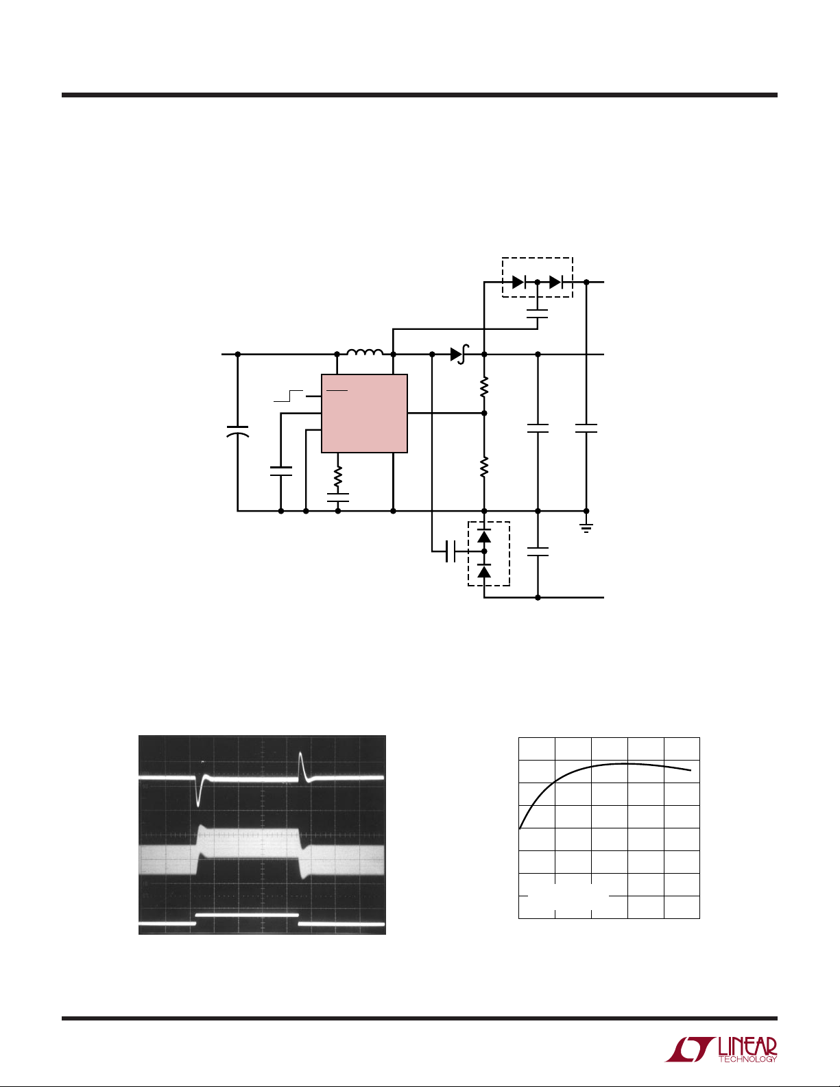
TYPICAL APPLICATIO
U
L1
V
IN
5V
OFF ON
C1
2.2µF
R
C
27.4k
C
C
270pF
C1: 2.2µF, X5R or X7R, 6.3V
C2: 2.2µF, X5R or X7R, 16V
D1: MICROSEMI UPS120 OR EQUIVALENT
L1: SUMIDA CR43-2R2
* EXPOSED PAD MUST ALSO BE GROUNDED
C
100nF
SS
2.2µH
65
V
IN
3
SHDN
LT1946A
1
V
C
GND*SS
Figure 1. 5V to 12V, 430mA Step-Up DC/DC Converter
SW
COMP
48
D1
R1
182k
2
FB
7
R2
21k
V
12V
430mA
C2
2.2µF
1946A TA01
OUT
Efficiency
sn1946a 1946afs
1
Page 2
LT1946A
PACKAGE/ORDER I FOR ATIO
UU
W
WWWU
ABSOLUTE AXI U RATI GS
(Note 1)
VIN Voltage .............................................................. 16V
SW Voltage ................................................–0.4V to 36V
FB Voltage .............................................................. 2.5V
Current into FB Pin ............................................... ±1mA
SHDN Voltage .......................................................... 16V
Maximum Junction Temperature .......................... 125°C
Operating Temperature
Range (Note 2) ....................................... – 40°C to 85°C
Storage Temperature Range ................. –65°C to 150°C
Lead Temperature (Soldering, 10 sec)..................300°C
ORDER PART
TOP VIEW
V
1
C
2
FB
3
SHDN
4
GND
MS8E PACKAGE
8-LEAD PLASTIC MSOP
EXPOSED PAD IS GROUND
(MUST BE SOLDERED TO PCB)
T
= 125°C, θJA = 40°C/W,
JMAX
= 10°C/W
θ
JC
Consult LTC Marketing for parts specified with wider operating temperature ranges.
8
7
6
5
SS
COMP
V
IN
SW
NUMBER
LT1946AEMS8E
MS8E PART
MARKING
LTYZ
ELECTRICAL CHARACTERISTICS
temperature range, otherwise specifications are at TA = 25°C. VIN = 3V, V
PARAMETER CONDITIONS MIN TYP MAX UNITS
Minimum Operating Voltage 2.45 2.6 V
Maximum Operating Voltage 16 V
Feedback Voltage 1.23 1.25 1.27 V
FB Pin Bias Current VFB = 1.25V (Note 3) ● 20 120 nA
Error Amp Transconductance ∆I = 2µA40µmhos
Error Amp Voltage Gain 300 V/V
Quiescent Current V
Quiescent Current in Shutdown V
Reference Line Regulation 2.6V ≤ VIN ≤ 16V 0.01 0.05 %/V
Switching Frequency 2.4 2.7 3 MHz
Switching Frequency in Foldback VFB = 0V 0.85 MHz
Maximum Duty Cycle ● 73 80 %
Switch Current Limit (Note 4) ● 1.5 2.1 3.1 A
Switch V
CESAT
Switch Leakage Current VSW = 5V 0.01 1 µA
Soft-Start Charging Current VSS = 0.5V 2.5 4 6 µA
SHDN Input Voltage High 2.4 V
SHDN Input Voltage Low 0.5 V
SHDN Pin Bias Current V
Note 1: Absolute Maximum Ratings are those values beyond which the life
of a device may be impaired.
Note 2: The LT1946AE is guaranteed to meet performance specifications
from 0°C to 70°C. Specifications over the –40°C to 85°C operating
= 2.5V, Not Switching 3.6 5 mA
SHDN
= 0V, VIN = 3V 0 1 µA
SHDN
ISW = 1A 240 340 mV
= 3V 16 32 µA
SHDN
= 0V 0 0.1 µA
V
SHDN
The ● denotes the specifications which apply over the full operating
= VIN unless otherwise noted. (Note 2)
SHDN
● 1.22 1.27 V
● 2.3 3.1 MHz
temperature range are assured by design, characterization and correlation
with statistical process controls.
Note 3: Current flows out of the FB pin.
Note 4: Current limit guaranteed by design and/or correlation to static test.
Current limit is independent of duty cycle and is guaranteed by design.
sn1946a 1946afs
2
Page 3

UW
TYPICAL PERFOR A CE CHARACTERISTICS
Feedback Pin Voltage Oscillator Frequency Current Limit
1.28
1.27
1.26
1.25
1.24
1.23
FEEDBACK VOLTAGE (V)
1.22
1.21
1.20
–50 –25 0 25 50 75 100 125
TEMPERATURE (°C)
1946A G01
Switch Saturation Voltage Quiescent Current
0.35
0.30
0.25
0.20
(V)
CESAT
0.15
V
0.10
0.05
0
0 0.2
0.4 0.6 0.8 1 1.2 1.4 1.6
SWITCH CURRENT (A)
1946A G04
3000
2700
2400
TA = –30°C TA = 100°C
2100
1800
1500
1200
900
600
OSCILLATOR FREQUENCY (kHz)
300
0
0 0.2
4.0
3.8
3.6
3.4
3.2
3.0
2.8
QUIESCENT CURRENT (mA)
2.6
2.4
2.2
–50 –25 0 25 50 75 100 125
0.4 0.6 0.8 1 1.2
FEEDBACK VOLTAGE (V)
TEMPERATURE (°C)
TA = 25°C
1946A G02
1946A G05
2.6
2.4
2.2
2.0
1.8
1.6
1.4
1.2
1.0
CURRENT LIMIT (A)
0.8
0.6
0.4
0.2
0
–50 –25
V
OUT
100mV/DIV
AC COUPLED
V
SW
10V/DIV
0V
0.5A/DIV
LT1946A
0 25 50 75 100 125
TEMPERATURE (°C)
Switching Waveforms for
Figure 1 Circuit
I
LI
100ns/DIV 1946A G06
1946A G03
V
100mV/DIV
AC COUPLED
0.5A/DIV
250mA
I
LOAD
150mA
Transient Response for
Figure 1 Circuit
OUT
I
LI
50µs/DIV 1946A G07
V
OUT
2V/DIV
200mA/DIV
V
SHDN
Start-Up Waveforms for
Figure 1 Circuit
I
IN
0A
5V
0V
R
= 250Ω 1ms/DIV 1946A G08
LOAD
sn1946a 1946afs
3
Page 4

LT1946A
U
UU
PI FU CTIO S
VC (Pin 1): Error Amplifier Output Pin. Tie external compensation network to this pin or use the internal compensation network by shorting the VC pin to the COMP pin.
External compensation consists of placing a resistor and
capacitor in series from VC to GND. Typical capacitor
range is from 90pF to 270pF. Typical resistor range is from
25k to 120k.
FB (Pin 2): Feedback Pin. Reference voltage is 1.25V.
Connect resistive divider tap here. Minimize trace area at
FB. Set V
SHDN (Pin 3): Shutdown Pin. Tie to 2.4V or more to enable
device. Ground to shut down. Do not float this pin.
GND (Pin 4, Exposed Pad): Ground. Tie both Pin 4 and
the exposed pad directly to local ground plane. The
ground metal to the exposed pad should be wide for better
heat dissipation. Multiple vias (local ground plane ↔
ground backplane) placed close to the exposed pad can
further aid in reducing thermal resistance.
according to V
OUT
= 1.25 • (1+R1/R2).
OUT
SW (Pin 5): Switch Pin. This is the collector of the internal
NPN power switch. Minimize the metal trace area connected to this pin to minimize EMI.
VIN (Pin 6): Input Supply Pin. Must be locally bypassed.
COMP (Pin 7): Internal Compensation Pin. Provides an
internal compensation network. Tie directly to the VC pin
for internal compensation. Tie to GND if not used.
SS (Pin 8): Soft-Start Pin. Place a soft-start capacitor
here. Upon start-up, 4µA of current charges the capacitor
to 1.5V. Use a larger capacitor for slower start-up. Leave
floating if not in use.
4
sn1946a 1946afs
Page 5

BLOCK DIAGRA
LT1946A
W
V
OUT
R1 (EXTERNAL)
FB
R2 (EXTERNAL)
SHUTDOWN
V
SHDN
SS V
4µA
1.25V
6
IN
REFERENCE
+
A1
–
+
0.5V
A3
÷ 3
–
23
FB
COMP
C
1 78
RAMP
GENERATOR
2.7MHz
OSCILLATOR
120k
90pF
COMPARATOR
–
A2
RQ
S
+
DRIVER
+
Σ
5
SW
Q1
0.01Ω
–
4
GND
EXPOSED
PAD
1946A F02
Figure 2. Block Diagram
sn1946a 1946afs
5
Page 6

LT1946A
OPERATIO
U
The LT1946A uses a constant frequency, current mode
control scheme to provide excellent line and load regulation. Please refer to Figure 2 for the following description
of the part’s operation. At the start of the oscillator cycle,
the SR latch is set, turning on the power switch Q1. The
switch current flows through the internal current sense
resistor generating a voltage. This voltage is added to a
stabilizing ramp and the resulting sum is fed into the
positive terminal of the PWM comparator A2. When this
voltage exceeds the level at the negative input of A2, the SR
latch is reset, turning off the power switch. The level at the
negative input of A2 (VC pin) is set by the error amplifier
(A1) and is simply an amplified version of the difference
between the feedback voltage and the reference voltage of
1.250V. In this manner, the error amplifier sets the correct
peak current level to keep the output in regulation.
Two functions are provided to enable a very clean start-up
for the LT1946A. Frequency foldback is used to reduce the
oscillator frequency by one-third when the FB pin is below
WUUU
APPLICATIO S I FOR ATIO
Inductor Selection
Several inductors that work well with the LT1946A are
listed in Table 1. This table is not complete, and there are
many other manufacturers and devices that can be used.
Consult each manufacturer for more detailed information
and for their entire selection of related parts, as many
different sizes and shapes are available. Ferrite core inductors should be used to obtain the best efficiency, as core
losses at 2.7MHz are much lower for ferrite cores than for
the cheaper powdered-iron ones. Choose an inductor that
can handle at least 1.5A without saturating, and ensure
that the inductor has a low DCR (copper-wire resistance)
to minimize I2R power losses. A 1.5µH to 4.7µH inductor
will be the best choice for most LT1946A designs. Note
that in some applications, the current handling requirements of the inductor can be lower, such as in the SEPIC
topology where each inductor only carries one-half of the
total switch current.
The inductors shown in Table 1 were chosen for small size.
For better efficiency, use similar valued inductors with a
larger volume.
a nominal value of 0.5V. This is accomplished via comparator A3. This feature reduces the minimum duty cycle
that the part can achieve thus allowing better control of the
switch current during start-up. When the FB pin voltage
goes above 0.5V, the oscillator returns to the normal
frequency of 2.7MHz. A soft-start function is also provided
by the LT1946A. When the part is brought out of shutdown, 4µA of current is sourced out of the SS pin. By
connecting an external capacitor to the SS pin, the rate of
voltage rise on the pin can be set. Typical values for the
soft-start capacitor range from 10nF to 200nF. The SS pin
directly limits the rate of rise on the VC pin, which in turn
limits the peak switch current. Current limit is not shown
in Figure 2. The switch current is constantly monitored and
not allowed to exceed the nominal value of 2.1A. If the
switch current reaches 2.1A, the SR latch is reset regardless of the output of comparator A2. This current limit
protects the power switch as well as various external
components connected to the LT1946A.
Table 1. Recommended Inductors - LT1946A
MAX Size
L DCR LxWxH
PART (µH) (mΩ) (mm) VENDOR
RLF5018-1R5M2R1 1.5 25 5.2x5.6x1.8 TDK
RLF5018-2R7M1R8 2.7 33 (847) 803-6100
RLF5018-4R7M1R4 4.7 45 www.tdk.com
RLF5018-100MR94 10.0 67
LPO1704-122MC 1.2 80 5.5x6.6x1.0 Coilcraft
LPO1704-222MC 2.2 120 (800) 322-2645
www.coilcraft.com
CR43-2R2 2.2 71 4.5x4.0x3.2 Sumida
CR43-3R3 3.3 86 (847) 956-0666
www.sumida.com
Capacitor Selection
Low ESR (equivalent series resistance) capacitors should
be used at the output to minimize the output ripple voltage.
Multilayer ceramic capacitors are an excellent choice, as
they have an extremely low ESR and are available in very
small packages. X5R dielectrics are preferred, followed by
X7R, as these materials retain the capacitance over wide
voltage and temperature ranges. A 2.2µF to 20µF output
sn1946a 1946afs
6
Page 7

WUUU
APPLICATIO S I FOR ATIO
capacitor is sufficient for most applications, but systems
with very low output currents may need only a 1µF or
smaller output capacitor. Solid tantalum or OSCON capacitors can be used, but they will occupy more board area
than a ceramic and will have a higher ESR. Always use a
capacitor with a sufficient voltage rating.
Ceramic capacitors also make a good choice for the input
decoupling capacitor, which should be placed as close as
possible to the LT1946A. A 2.2µF to 4.7µF input capacitor
is sufficient for most applications. Table 2 shows a list of
several ceramic capacitor manufacturers. Consult the
manufacturers for detailed information on their entire
selection of ceramic parts.
LT1946A
V
OUT
200mV/DIV
AC COUPLED
I
L1
0.5A/DIV
R
= 2.5k
C
Figure 3a. Transient Response Shows Excessive Ringing
50µs/DIV
1946A F03a
Table 2. Ceramic Capacitor Manufacturers
Taiyo Yuden (408) 573-4150 www.t-yuden.com
AVX (803) 448-9411 www.avxcorp.com
Murata (714) 852-2001 www.murata.com
Compensation
To compensate the feedback loop of the LT1946A, a series
resistor-capacitor network should be connected from the
COMP pin to GND. For most applications, a capacitor in the
range of 90pF to 470pF will suffice. A good starting value
for the compensation capacitor, CC, is 270pF. The compensation resistor, RC, is usually in the range of 20k to
100k. A good technique to compensate a new application
is to use a 100k potentiometer in place of RC, and use a
270pF capacitor for CC. By adjusting the potentiometer
while observing the transient response, the optimum
value for RC can be found. Figures 3a-3c illustrate this
process for the circuit of Figure 1. Figure 3a shows the
transient response with RC equal to 2.5k. The phase
margin is poor as evidenced by the excessive ringing in the
output voltage and inductor current. In Figure 3b the value
of RC is increased to 6.5k, which results in a more damped
response. Figure 3c shows the results when RC is increased further to 27.4k. The transient response is nicely
damped and the compensation procedure is complete.
The COMP pin provides access to an internal resistor
(120k) and capacitor (90pF). For some applications, these
values will suffice and no external RC and CC will be
needed.
V
OUT
200mV/DIV
AC COUPLED
I
L1
0.5A/DIV
R
= 6.5k
C
Figure 3b. Transient Response is Better
V
OUT
200mV/DIV
AC COUPLED
I
L1
0.5A/DIV
= 27.4k
R
C
Figure 3c. Transient Response is Well Damped
50µs/DIV
50µs/DIV
1946A F03b
1946A F03c
Compensation-Theory
Like all other current mode switching regulators, the
LT1946A needs to be compensated for stable and efficient
operation. Two feedback loops are used in the LT1946A:
a fast current loop which does not require compensation,
and a slower voltage loop which does. Standard bode plot
analysis can be used to understand and adjust the voltage
feedback loop.
sn1946a 1946afs
7
Page 8

LT1946A
Z
VR
VL
IN L
OUT
3
2
2
2
=
•
•• •π
WUUU
APPLICATIO S I FOR ATIO
As with any feedback loop, identifying the gain and phase
contribution of the various elements in the loop is critical.
Figure 4 shows the key equivalent elements of a boost
converter. Because of the fast current control loop, the
power stage of the IC, inductor, and diode have been
replaced by the equivalent transconductance amplifier
GMP. GMP acts as a current source where the output
current is proportional to the VC voltage. Note that the
maximum output current of GMP is finite due to the current
limit in the IC.
From Figure 4, the DC gain, poles and zeroes can be
calculated as follows:
Output Pole:
P
1
Error Amp Pole:
Error Amp Zero:
125.
A
DC Gain:
R
C
C
C
=
V
OUT
–
G
MP
+
V
C
R
O
P
G
2=•• •π
2
Z
1
MA
2
RC
L OUT
1
2=•• •π
RC
OC
1
RC
2=•• •π
GRGR
••••
MA O MP L
+
–
CC
1.250V
REFERENCE
ESR
C
OUT
R
1
R
2
V
OUT
R
L
ESR Zero:
Z
2
2=•• •π
1
ESR C
OUT
RHP Zero:
F
S
>
High Frequency Pole:
P
3
3
Using the circuit of Figure 1 as an example, Table 3 shows
the parameters used to generate the bode plot shown in
Figure 5.
Table 3. Bode Plot Parameters
Parameter Value Units Comment
R
L
C
OUT
R
O
C
C
R
C
V
OUT
V
IN
G
MA
G
MP
L 2.2 µH Application Specific
F
S
ESR 10 mΩ Not Adjustable
28 Ω Application Specific
2.2 µF Application Specific
10 MΩ Not Adjustable
270 pF Adjustable
27.4 kΩ Adjustable
12 V Application Specific
5 V Application Specific
40 µmho Not Adjustable
5 mho Not Adjustable
2.7 MHz Not Adjustable
From Figure 5, the phase when the gain reaches 0dB is
122° giving a phase margin of 58°. This is more than
adequate. The cross-over frequency is 90kHz, which is
about 30 times lower than the frequency of the right half
plane zero Z2. It is important that the cross-over frequency
be at least 3 times lower than the frequency of the RHP zero
to achieve adequate phase margin.
GMA: TRANSCONDUCTANCE AMPLIFIER INSIDE IC
: POWER STAGE TRANSCONDUCTANCE AMPLIFIER
G
MP
: OUTPUT CAPACITOR
C
OUT
: OUTPUT RESISTANCE DEFINED AS V
R
L
R1, R2: FEEDBACK RESISTOR DIVIDER NETWORK
: OUTPUT RESISTANCE OF G
R
O
RC: COMPENSATION RESISTOR
: COMPENSATION CAPACITOR
C
C
MA
Figure 4. Boost Converter Equivalent Model
8
DIVIDED BY I
OUT
LOAD
(MAX)
sn1946a 1946afs
Page 9

WUUU
APPLICATIO S I FOR ATIO
LT1946A
100
50
GAIN (f)
0
–50
100 10k 100k 1M
0
–100
PHASE (f)
–180
–200
100 10k 100k 1M
1k
FREQUENCY (Hz)
1946A FO5a
58°
1k
FREQUENCY (Hz)
1946A FO5b
Figure 5. Gain and Phase Plots of Figure 1 Circuit
Setting Output Voltage
To set the output voltage, select the values of R1 and R2
(see Figure 1) according to the following equation:
RR
12
V
OUT
.
125
–
1=
V
A good range for R2 is from 5k to 30k.
Layout Hints
The high speed operation of the LT1946A demands careful
attention to board layout. You will not get advertised
performance with careless layouts. Figure 6 shows the
recommended component placement for a boost converter.
GROUND PLANE
R1
SHUTDOWN
C
C
R
C
R2
1
2
3
4
CSS
LT1946A
C1
+
8
7
6
5
V
IN
L1
Diode Selection
A Schottky diode is recommended for use with the LT1946A.
The Microsemi UPS120 is a very good choice. Where the
input to output voltage differential exceeds 20V, use the
UPS140 (a 40V diode). These diodes are rated to handle an
average forward current of 1A. For applications where the
average forward current of the diode is less than 0.5A, an
ON Semiconductor MBR0520 diode can be used.
MULTIPLE
VIAs
GND
NOTE: DIRECT HIGH CURRENT PATHS USING WIDE PC TRACES. MINIMIZE TRACE AREA AT
PIN 1(V
) AND PIN 2(FB). USE MULTIPLE VIAS TO TIE PIN 4 COPPER TO GROUND PLANE. USE
C
VIAS AT ONE LOCATION ONLY TO AVOID INTRODUCING SWITCHING CURRENTS INTO THE
GROUND PLANE.
C2
V
OUT
19949 F04
Figure 6. Recommended Component
Placement for Boost Converter
sn1946a 1946afs
9
Page 10
LT1946A
A
VDD
LOAD CURRENT (mA)
EFFICIENCY (%)
1946A TA04
90
85
80
75
70
65
60
55
50
0 100 200 300 400 500
VON LOAD = 5mA
V
OFF
LOAD = 10mA
TYPICAL APPLICATIO S
Low Profile (<1.1mm Tall) Triple Output TFT Supply (10V, –10V, 20V)
U
V
IN
5V
V
IN
OFF ON
+
C1
4.7µF
C
SS
100nF
C1–C6: X5R or X7R
C1: 4.7µF, 6.3V
C2: 2× 10µF, 10V
C3: 1µF, 25V
C4: 2.2µF, 10V
C5–C6: 0.1µF, 10V
D1: MICROSEMI UPS120 OR EQUIVALENT
D2–D5: ZETEX BAT54S OR EQUIVALENT
L1: COILCRAFT LP01704-152MC
* EXPOSED PAD MUST ALSO BE GROUNDED
3
8
7
SHDN
SS
COMP
V
L1
1.5µH
65
SW
GND*
2
FB
4
LT1946A
C
1
R
C
59k
C
150pF
C
C6
0.1µF
D2 D3
C5
0.1µF
D1
R1
75k
C2
20µF
R2
10.5k
D4
D5
C4
2.2µF
V
20V
5mA
A
10V
475mA
C3
1µF
V
–10V
10mA
1946A TA02
ON
VDD
OFF
A
VDD
50mV/DIV
AC COUPLED
I
LI
0.5A/DIV
LOAD
A
VDD
10
350mA
200mA
Transient Response
100µs/DIV 1946A TA03
Efficiency
sn1946a 1946afs
Page 11

U
TYPICAL APPLICATIO S
Triple Output TFT Supply Uses SEPIC Topology for Output Disconnect
LT1946A
V
12V ± 10%
IN
+
C1
2.2µF
100nF
C1–C5: X5R or X7R
C1: 2.2µF, 6.3V
C2: 2× 10µF, 16V
C3: 1µF, 25V
C4: 0.22µF, 25V
C5: 0.22µF, 16V
D2
C4
D3
L1
10µH
65
V
IN
OFF ON
C
SS
3
SHDN
8
LT1946A
SS
1
V
C
COMP
GND*
7
D1: MICROSEMI UPS120 OR EQUIVALENT
D2–D3: CENTRAL SEMI CMDSH-3
L1–L2: TDK RLF5018-100MR94
* EXPOSED PAD MUST ALSO BE GROUNDED
SW
C3
1µF
2
FB
L2
10µH
4
0.22µF
C5
0.22µF
D1
R1
84.5k
R2
9.76k
V
23V
10mA
V
–12V
10mA
A
12V
250mA
C2
20µF
1946A TA09
ON
OFF
VDD
MS8E Package
8-Lead Plastic MSOP
(Reference LTC DWG # 05-08-1662)
2.794 ± 0.102
(.110 ± .004)
5.23
(.206)
MIN
0.42 ± 0.04
(.0165 ± .0015)
TYP
RECOMMENDED SOLDER PAD LAYOUT
NOTE:
1. DIMENSIONS IN MILLIMETER/(INCH)
2. DRAWING NOT TO SCALE
3. DIMENSION DOES NOT INCLUDE MOLD FLASH, PROTRUSIONS OR GATE BURRS.
MOLD FLASH, PROTRUSIONS OR GATE BURRS SHALL NOT EXCEED 0.152mm (.006") PER SIDE
4. DIMENSION DOES NOT INCLUDE INTERLEAD FLASH OR PROTRUSIONS.
INTERLEAD FLASH OR PROTRUSIONS SHALL NOT EXCEED 0.152mm (.006") PER SIDE
5. LEAD COPLANARITY (BOTTOM OF LEADS AFTER FORMING) SHALL BE 0.102mm (.004") MAX
2.083
(.082 ± .004)
0.65
(.0256)
BSC
0.889 ± 0.127
(.035 ± .005)
3.2 – 3.45
± 0.102
(.126 – .136)
GAUGE PLANE
0.18
(.077)
0.254
(.010)
DETAIL “A”
DETAIL “A”
° – 6° TYP
0
Information furnished by Linear Technology Corporation is believed to be accurate and reliable.
However, no responsibility is assumed for its use. Linear Technology Corporation makes no representation that the interconnection of its circuits as described herein will not infringe on existing patent rights.
0.53 ± 0.015
(.021 ± .006)
SEATING
PLANE
3.00 ± 0.102
(.118 ± .004)
(NOTE 3)
4.88
± 0.1
(.192 ± .004)
0.22 – 0.38
(.009 – .015)
1.10
(.043)
MAX
8
12
0.65
(.0256)
BCS
BOTTOM VIEW OF
NOTE 4
0.86
REF
0.13 ± 0.05
(.005 ± .002)
MSOP (MS8E) 1001
EXPOSED PAD OPTION
1
8
sn1946a 1946afs
2.06 ± 0.102
(.080 ± .004)
1.83 ± 0.102
(.072 ± .004)
0.52
7
(.206)
6
5
REF
3.00 ± 0.102
(.118 ± .004)
4
3
(.34)
11
Page 12

LT1946A
TYPICAL APPLICATIO S
Low Profile (<1.1mm Tall) Triple Output TFT Supply (8V, –8V, 24V)
U
V
IN
3.3V
3
OFF ON
+
C1
4.7µF
C
SS
100nF
C1–C8: X5R or X7R
C1: 4.7µF, 6.3V
C2: 2× 10µF, 10V
C3: 2.2µF, 10V
C4: 1µF, 25V
C5, C6, C8: 0.1µF, 10V
C7: 0.1µF, 16V
D1: MICROSEMI UPS120 OR EQUIVALENT
D2–D7: ZETEX BAT54S OR EQUIVALENT
L1: COILCRAFT LP01704-122MC
* EXPOSED PAD MUST ALSO BE GROUNDED
8
7
SHDN
SS
COMP
D2 D3
L1
1.2µH
56
LT1946A
SW
GND*
2
FB
4
V
IN
V
C
1
Transient Response
C5
0.1µF
C8
0.1µF
D4 D5
C6
0.1µF
C7
0.1µF
V
ON
23V
5mA
Efficiency
D1
R2
28.7k
C2
20µF
R3
5.23k
D7
D6
C3
2.2µF
AV
8V
375mA
C4
1µF
V
OFF
–8V
10mA
1946A TA05
DD
90
85
80
75
70
65
EFFICIENCY (%)
60
VON LOAD = 5mA
55
50
LOAD = 10mA
V
OFF
0 100 200 300 400
A
LOAD CURRENT (mA)
VDD
1946A TA06
Start-Up Waveforms
A
VDD
50mV/DIV
AC COUPLED
I
0.5A/DIV
350mA
I
LOAD
200mA
LI
50µs/DIV
1946A TA07 1946A TA08
A
VDD
5V/DIV
V
10V/DIV
V
OFF
5V/DIV
0.5A/DIV
ON
I
IN
RELATED PARTS
PART NUMBER DESCRIPTION COMMENTS
LT1613 550mA (ISW), 1.4MHz, Step-Up DC/DC Converter VIN = 0.9V to 10V, V
LT1615/LT1615-1 300mA/0.75mA (ISW), Constant Off-Time Step-Up VIN = 1V to 15V, V
DC/DC Converter
LT1930/LT1930A 1A (ISW), 1.2MHz/2.2MHz, Step-Up DC/DC Converter VIN = 2.6V to 16V, V
LT1946 1.5A (ISW), 1.2MHz, Step-Up DC/DC Converter VIN = 2.45V to 16V, V
LT1961 1.5A (ISW), 1.25MHz, Step-Up DC/DC Converter VIN = 3V to 25V, V
ThinSOT is a trademark of Linear Technology Corporation.
Linear Technology Corporation
12
1630 McCarthy Blvd., Milpitas, CA 95035-7417
(408) 432-1900 ● FAX: (408) 434-0507 ● www.linear.com
OUT
OUT
1ms/DIV
to 34V, IQ = 3mA, ISD < 1µA, ThinSOT
OUT
TM
to 34V, IQ = 20µA, ISD < 1µA, ThinSOT
to 34V, IQ = 4.2mA/5.5mA, ISD < 1µA, ThinSOT
OUT
to 34V, IQ = 3.2mA, ISD < 1µA, MS8
OUT
to 35V, IQ = 0.9mA, ISD < 6µA, MS8E
sn1946a 1946afs
LT/TP 1102 2K • PRINTED IN USA
LINEAR TECHNOLOGY CORPORATION 2001
 Loading...