

FEATURES
LT1932
Constant-Current DC/DC
LED Driver in ThinSOT
U
DESCRIPTIO
■
Up to 80% Efficiency
■
Inherently Matched LED Current
■
Adjustable Control of LED Current
■
Drives Five White LEDs from 2V
■
Drives Six White LEDs from 2.7V
■
Drives Eight White LEDs from 3V
■
Disconnects LEDs In Shutdown
■
1.2MHz Fixed Frequency Switching
■
Uses Tiny Ceramic Capacitors
■
Uses Tiny 1mm-Tall Inductors
■
Regulates Current Even When VIN > V
■
Operates with VIN as Low as 1V
■
Low Profile (1mm) ThinSOTTM Package
U
APPLICATIO S
■
Cellular Telephones
■
Handheld Computers
■
Digital Cameras
■
Portable MP3 Players
■
Pagers
OUT
The LT®1932 is a fixed frequency step-up DC/DC converter
designed to operate as a constant-current source. Because it directly regulates output current, the LT1932 is
ideal for driving light emitting diodes (LEDs) whose light
intensity is proportional to the current passing through
them, not the voltage across their terminals.
With an input voltage range of 1V to 10V, the device works
from a variety of input sources. The LT1932 accurately
regulates LED current even when the input voltage is
higher than the LED voltage, greatly simplifying batterypowered designs. A single external resistor sets LED
current between 5mA and 40mA, which can then be easily
adjusted using either a DC voltage or a pulse width
modulated (PWM) signal. When the LT1932 is placed in
shutdown, the LEDs are disconnected from the output,
ensuring a quiescent current of under 1µA for the entire
circuit. The device’s 1.2MHz switching frequency permits
the use of tiny, low profile chip inductors and capacitors to
minimize footprint and cost in space-conscious portable
applications.
, LTC and LT are registered trademarks of Linear Technology Corporation.
ThinSOT is a trademark of Linear Technology Corporation.
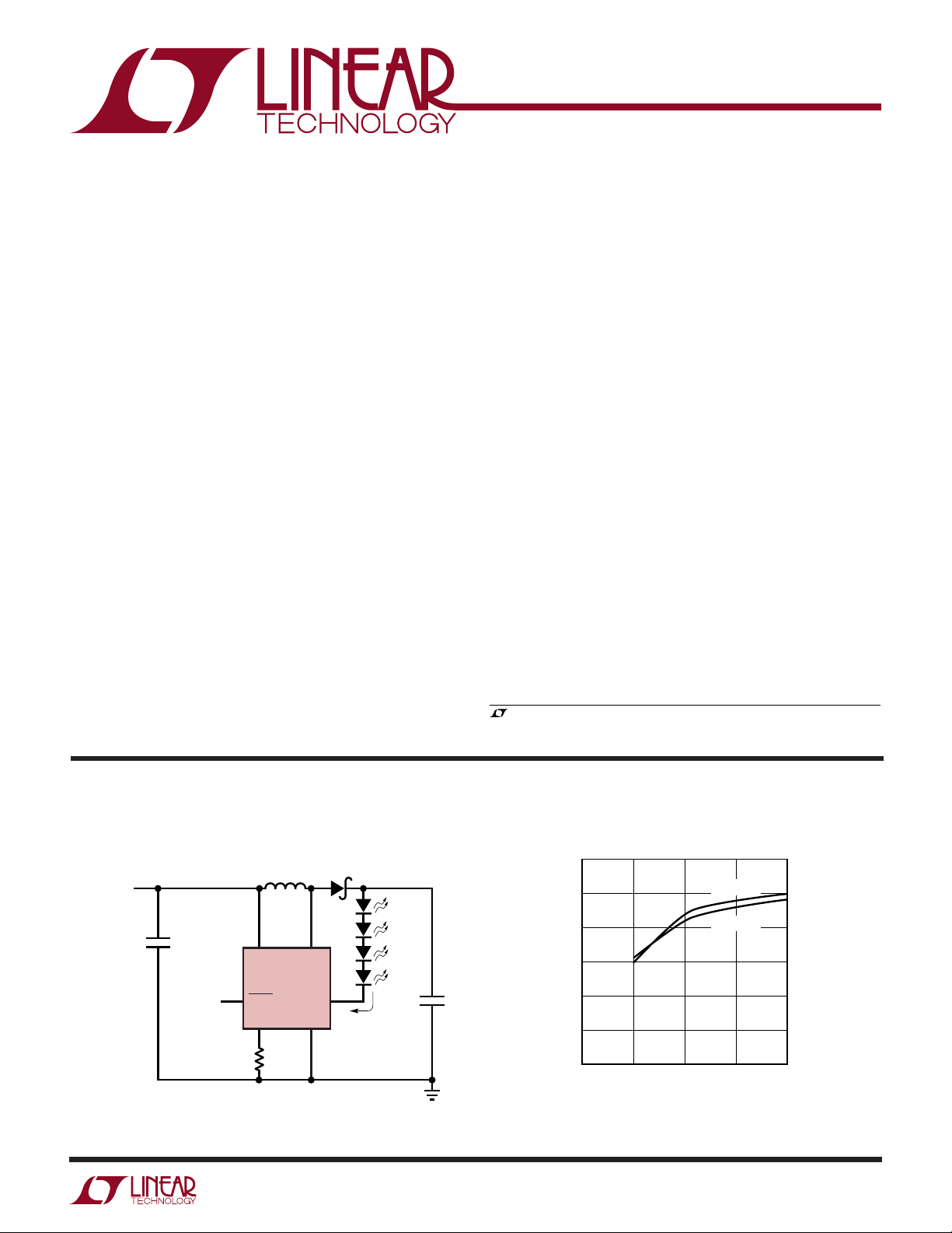
TYPICAL APPLICATIO
Li-Ion Driver for Four White LEDs Efficiency
L1
V
2.7V TO 4.2V
IN
C1
4.7µF
PWM
DIMMING
CONTROL
C1: TAIYO YUDEN JMK212BJ475
C2: TAIYO YUDEN EMK212BJ105
D1:ZETEX ZHCS400
L1: SUMIDA CLQ4D106R8 OR PANASONIC ELJEA6R8
6.8µH
61
V
IN
LT1932
SHDN
R
SET
4
R
SET
1.50k
SW
GND
LED
2
U
D1
35
15mA
C2
1µF
1932 TA01
85
80
75
70
EFFICIENCY (%)
65
60
55
0
VIN = 4.2V
VIN = 2.7V
5101520
LED CURRENT (mA)
1932 TA02
1932f
1
LT1932
WWWU
ABSOLUTE AXI U RATI GS
PACKAGE/ORDER I FOR ATIO
UU
W
(Note 1)
VIN Voltage ............................................................. 10V
SHDN Voltage ......................................................... 10V
SW Voltage ............................................................. 36V
LED Voltage ............................................................. 36V
R
Voltage ............................................................. 1V
SET
Junction Temperature.......................................... 125°C
Operating Temperature Range (Note 2) .. – 40°C to 85°C
Storage Temperature Range ................. –65°C to 150°C
TOP VIEW
SW 1
GND 2
LED 3
S6 PACKAGE
6-LEAD PLASTIC SOT-23
T
= 125°C, θJA = 250°C/ W
JMAX
6 V
IN
5 SHDN
4 R
SET
ORDER PART
NUMBER
LT1932ES6
S6 PART MARKING
LTST
Lead Temperature (Soldering, 10 sec)..................300°C
Consult LTC Marketing for parts specified with wider operating temperature ranges.
ELECTRICAL CHARACTERISTICS
range, otherwise specifications are at TA = 25°C. VIN = 1.2V, V
PARAMETER CONDITIONS MIN TYP MAX UNITS
Minimum Input Voltage 1V
Quiescent Current V
V
R
Pin Voltage R
SET
LED Pin Voltage R
LED Pin Current R
R
R
R
LED Pin Current Temperature Coefficient I
Switching Frequency VIN = 1V 0.8 1.2 1.6 MHz
Maximum Switch Duty Cycle ● 90 95 %
Switch Current Limit 400 550 780 mA
Switch V
CESAT
SHDN Pin Current V
Start-Up Threshold (SHDN Pin) 0.85 V
Shutdown Threshold (SHDN Pin) 0.25 V
Switch Leakage Current Switch Off, VSW = 5V 0.01 5 µA
LED
ISW = 300mA 150 200 mV
V
The ● denotes specifications that apply over the full operating temperature
= 1.2V, unless otherwise noted.
SHDN
= 0.2V 1.2 1.6 mA
RSET
= 0V 0.1 1.0 µA
SHDN
= 1.50k 100 mV
SET
= 1.50k, VIN < V
SET
= 562Ω, VIN = 1.5V 33 38 45 mA
SET
= 750Ω, VIN = 1.2V 25 30 36 mA
SET
= 1.50k, VIN = 1.2V 12.5 15 17.5 mA
SET
= 4.53k, VIN = 1.2V 5 mA
SET
= 15mA –0.02 mA/°C
= 0V 0 0.1 µA
SHDN
= 2V 15 30 µA
SHDN
(Figure 1) 120 180 mV
OUT
Note 1: Absolute Maximum Ratings are those values beyond which the life of
a device may be impaired.
Note 2: The LT1932E is guaranteed to meet specifications from 0°C to 70°C.
Specifications over the –40°C to 85°C operating temperature range are
assured by design, characterization and correlation with statistical process
controls.
2
1932f
UW
INPUT VOLTAGE (V)
0
LED CURRENT (mA)
35
6
1932 G06
20
10
24
5
0
40
45
50
30
25
15
810
R
SET
= 750Ω
R
SET
= 562Ω
R
SET
= 1.50k
R
SET
= 4.53k
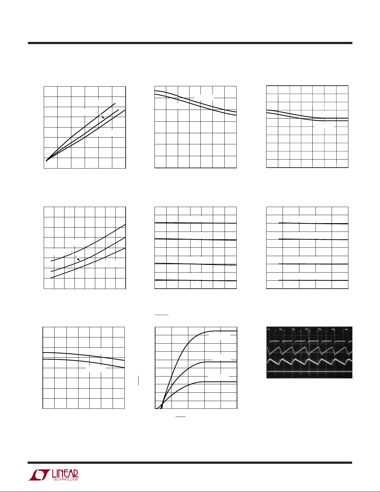
TYPICAL PERFOR A CE CHARACTERISTICS
LT1932
Switch Saturation Voltage (V
400
350
300
250
200
150
100
50
SWITCH SATURATION VOLTAGE (mV)
0
100 200 400
0
SWITCH CURRENT (mA)
TJ = 125°C
TJ = 25°C
300
TJ = –50°C
CESAT
500
1932 G01
600
)
Switch Current Limit Switching Frequency
700
600
500
400
300
PEAK CURRENT (mA)
200
100
0
–50
LED Pin Voltage LED Current
400
350
300
250
200
TJ = 25°C
150
LED PIN VOLTAGE (mV)
100
50
0
510 20
0
LED CURRENT (mA)
TJ = 125°C
15 25
T
= –50°C
J
4030 35
1932 G04
50
45
40
35
30
25
20
LED CURRENT (mA)
15
10
5
0
–50
VIN = 1.2V
VIN = 10V
50 100 125
–25 0
–25 0 50
25 75
TEMPERATURE (°C)
R
= 562Ω
SET
R
= 750Ω
SET
R
= 1.50k
SET
R
= 4.53k
SET
25
TEMPERATURE (°C)
1932 G02
75 100 125
1932 G05
2.0
1.8
1.6
1.4
1.2
1.0
0.8
0.6
0.4
SWITCHING FREQUENCY (MHz)
0.2
0
–50
–25
25
0
TEMPERATURE (°C)
LED Current
VIN = 10V
VIN = 1.2V
50
100
125
1932 G03
75
2.00
1.75
1.50
1.25
1.00
0.75
0.50
QUIESCENT CURRENT (mA)
0.25
Quiescent Current SHDN Pin Current
50
45
40
0
–25 0 50
–50
VIN = 10V
VIN = 1.2V
25
TEMPERATURE (°C)
75 100 125
1932 G07
35
30
25
20
SHDN PIN CURRENT
15
10
5
0
2
0
SHDN PIN VOLTAGE (V)
Switching Waveforms
V
= –50°C
T
J
TJ = 25°C
TJ = 125°C
6
8
4
10
1932 G08
SW
10V/DIV
I
200mA/DIV
V
OUT
20mV/DIV
AC COUPLED
I
LED
10mA/DIV
L1
VIN = 3V 0.5µs/DIV
4 WHITE LEDs
I
= 15mA
LED
CIRCUIT ON FIRST PAGE
OF THIS DATA SHEET
1093 G09
1932f
3
LT1932
U
UU
PI FU CTIO S
SW (Pin 1): Switch Pin. This is the collector of the internal
NPN power switch. Minimize the metal trace area connected to this pin to minimize EMI.
GND (Pin 2): Ground Pin. Tie this pin directly to local
ground plane.
LED (Pin 3): LED Pin. This is the collector of the internal
NPN LED switch. Connect the cathode of the bottom LED
to this pin.
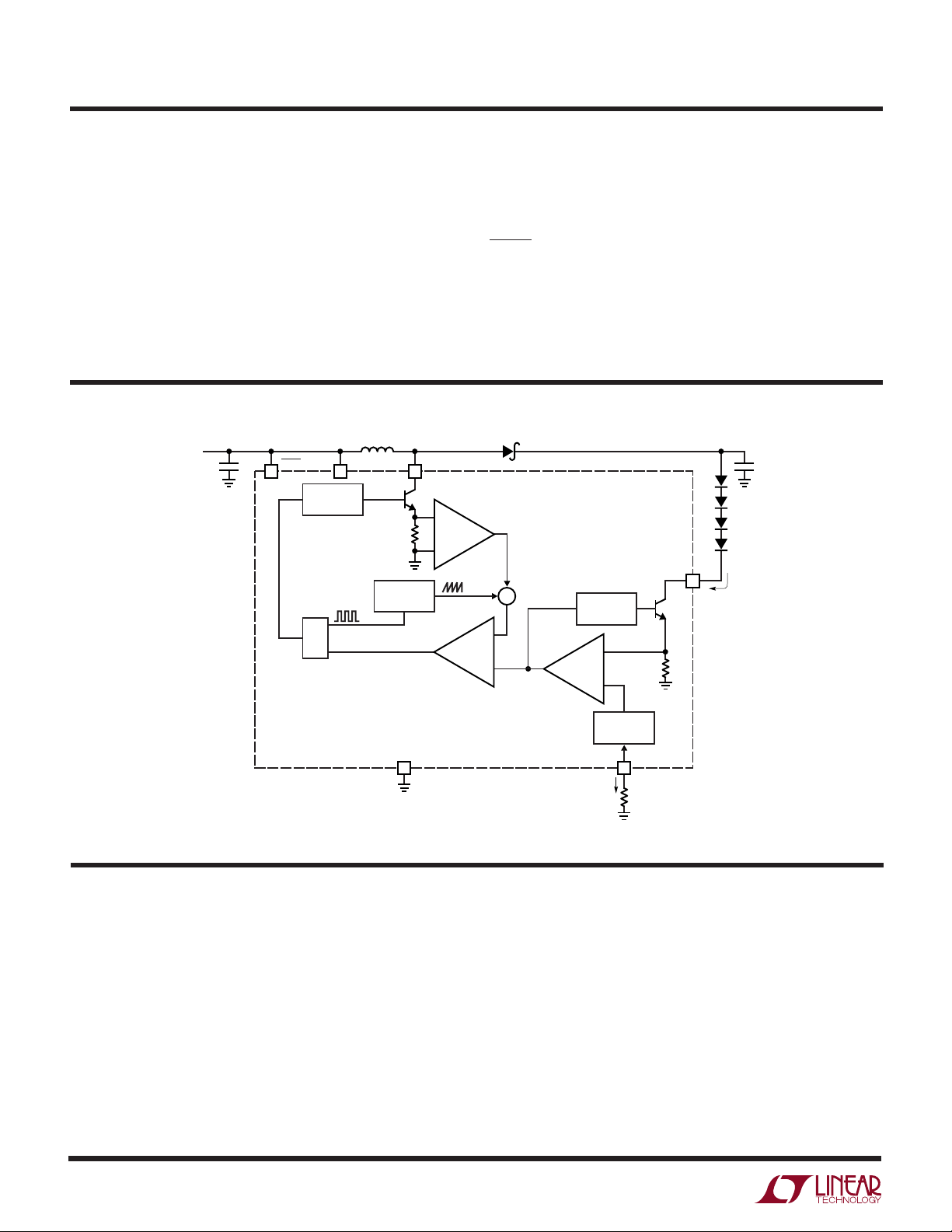
W
BLOCK DIAGRA
V
IN
SHDN
C1
5
DRIVER
S
Q
R
L1
V
IN
6
1
Q1
0.04Ω
1.2MHz
OSCILLATOR
SW
+
×5
–
R
(Pin 4): A resistor between this pin and ground
SET
programs the LED current (that flows into the LED pin).
This pin is also used to provide LED dimming.
SHDN (Pin 5): Shutdown Pin. Tie this pin higher than
0.85V to turn on the LT1932; tie below 0.25V to turn it off.
VIN (Pin 6): Input Supply Pin. Bypass this pin with a
capacitor to ground as close to the device as possible.
D1
+
Σ
+
+
A2
–
DRIVER
–
A1
+
V
OUT
C2
LED
3
I
Q2
LED
2
GND
Figure 1. LT1932 Block Diagram
U
OPERATIO
The LT1932 uses a constant frequency, current mode
control scheme to regulate the output current, I
Operation can be best understood by referring to the
block diagram in Figure 1. At the start of each oscillator
cycle, the SR latch is set, turning on power switch Q1. The
signal at the noninverting input of the PWM comparator
A2 is proportional to the switch current, summed together with a portion of the oscillator ramp. When this
signal reaches the level set by the output of error amplifier
A1, comparator A2 resets the latch and turns off the
LED
.
LED CURRENT
REFERENCE
4
R
SET
I
SET
R
SET
1932 F01
power switch. In this manner, A1 sets the correct peak
current level to keep the LED current in regulation. If A1’s
output increases, more current is delivered to the output;
if it decreases, less current is delivered. A1 senses the
LED current in switch Q2 and compares it to the current
reference, which is programmed using resistor R
R
pin is regulated to 100mV and the output current,
SET
I
, is regulated to 225 • I
LED
. Pulling the R
SET
SET
. The
SET
pin higher
than 100mV will pull down the output of A1, turning off
power switch Q1 and LED switch Q2.
1932f
4
WUUU
APPLICATIO S I FOR ATIO
LT1932
Inductor Selection
Several inductors that work well with the LT1932 are listed
in Table 1. Many different sizes and shapes are available.
Consult each manufacturer for more detailed information
and for their entire selection of related parts. As core
losses at 1.2MHz are much lower for ferrite cores that for
the cheaper powdered-iron ones, ferrite core inductors
should be used to obtain the best efficiency. Choose an
inductor that can handle at least 0.5A and ensure that the
inductor has a low DCR (copper wire resistance) to minimize I2R power losses. A 4.7µH or 6.8µH inductor will be
a good choice for most LT1932 designs.
Table 1. Recommended Inductors
MAX MAX
L DCR HEIGHT
PART (µH) (mΩ) (mm) VENDOR
ELJEA4R7 4.7 180 2.2 Panasonic
ELJEA6R8 6.8 250 2.2 (714) 373-7334
www.panasonic.com
LQH3C4R7M24 4.7 260 2.2 Murata
LQH3C100M24 10 300 2.2 (814) 237-1431
www.murata.com
LB2016B4R7 4.7 250 1.6 Taiyo Yuden
LB2016B100 6.8 350 1.6 (408) 573-4150
www.t-yuden.com
CMD4D06-4R7 4.7 216 0.8 Sumida
CMD4D06-6R8 6.8 296 0.8 (847) 956-0666
CLQ4D10-4R7 4.7 162 1.2 www.sumida.com
CLQ4D10-6R8 6.8 195 1.2
efficiency by up to 12% over the smaller, thinner ones.
Keep this in mind when choosing an inductor.
The value of inductance also plays an important role in the
overall system efficiency. While a 1µH inductor will have
a lower DCR and a higher current rating than the 6.8µH
version of the same part, lower inductance will result in
higher peak currents in the switch, inductor and diode.
Efficiency will suffer if inductance is too small. Figure 3
shows the efficiency of the Typical Application on the front
page of this data sheet, with several different values of the
same type of inductor (Panasonic ELJEA). The smaller
values give an efficiency 3% to 5% lower than the 6.8µH
value.
85
PANASONIC
80
75
70
EFFICIENCY (%)
65
60
55
SUMIDA
CLQ4D10-6R8
TAIYO YUDEN
LB2016B6R8
0
TAIYO YUDEN
LB2012B6R8
5101520
LED CURRENT (mA)
Figure 2. Efficiency for Several Different Inductor Types
ELJEA6R8
SUMIDA
CMD4D06-6R8
VIN = 3.6V
4 WHITE LEDs
ALL ARE 10µH
INDUCTORS
1932 F02
Inductor Efficiency Considerations
Many applications have thickness requirements that restrict component heights to 1mm or 2mm. There are 2mm
tall inductors currently available that provide a low DCR
and low core losses that help provide good overall efficiency. Inductors with a height of 1mm (and less) are
becoming more common, and a few companies have
introduced chip inductors that are not only thin, but have
a very small footprint as well. While these smaller inductors will be a necessity in some designs, their smaller size
gives higher DCR and core losses, resulting in lower
efficiencies. Figure 2 shows efficiency for the Typical
Application circuit on the front page of this data sheet, with
several different inductors. The larger devices improve
85
80
75
4.7µH
70
EFFICIENCY (%)
65
60
55
0
22µH
6.8µH
2.2µH
VIN = 3.6V
4 WHITE LEDs
PANASONIC ELJEA
INDUCTORS
5101520
LED CURRENT (mA)
1932 F03
Figure 3. Efficiency for Several Different Inductor Values
1932f
5

LT1932
WUUU
APPLICATIO S I FOR ATIO
Capacitor Selection
Low ESR (equivalent series resistance) capacitors should
be used at the output to minimize the output ripple
voltage. Because they have an extremely low ESR and are
available in very small packages, multilayer ceramic capacitors are an excellent choice. X5R and X7R type
capacitors are preferred because they retain their capacitance over wider voltage and temperature ranges than
other types such as Y5V or Z5U. A 1µF or 2.2µF output
capacitor is sufficient for most applications. Always use a
capacitor with a sufficient voltage rating. Ceramic capacitors do not need to be derated (do not buy a capacitor with
a rating twice what your application needs). A 16V ceramic capacitor is good to more than 16V, unlike a 16V
tantalum, which may be good to only 8V when used in
certain applications. Low profile ceramic capacitors with
a 1mm maximum thickness are available for designs
having strict height requirements.
Ceramic capacitors also make a good choice for the input
decoupling capacitor, which should be placed as close as
possible to the LT1932. A 2.2µF or 4.7µF input capacitor
is sufficient for most applications. Table 2 shows a list of
several ceramic capacitor manufacturers. Consult the
manufacturers for detailed information on their entire
selection of ceramic parts.
Table 2. Recommended Ceramic Capacitor Manufacturers
VENDOR PHONE URL
Taiyo Yuden (408) 573-4150 www.t-yuden.com
Murata (814) 237-1431 www.murata.com
Kemet (408) 986-0424 www.kemet.com
Diode Selection
turned off (typically less than one-third the time), so a 0.4A
or 0.5A diode will be sufficient for most designs.
Table 3. Recommended Schottky Diodes
PART VENDOR
MBR0520 ON Semiconductor
MBR0530 (800) 282-9855
MBR0540 www.onsemi.com
ZHCS400 Zetex
ZHCS500 (631) 543-7100
www.zetex.com
Programming LED Current
The LED current is programmed with a single resistor
connected to the R
pin (see Figure 1). The R
SET
SET
pin is
internally regulated to 100mV, which sets the current
flowing out of this pin, I
LT1932 regulates the current into the LED pin, I
times the value of I
SET
, equal to 100mV/R
SET
SET
LED
. The
, to 225
. For the best accuracy, a 1% (or
better) resistor value should be used. Table 4 shows
several typical 1% R
values, use the following equation to choose R
R
SET
Table 4. R
=
SET
22501•
Resistor Values
I
(mA) R
LED
40 562Ω
30 750Ω
20 1.13k
15 1.50k
10 2.26k
5 4.53k
values. For other LED current
SET
V
.
I
LED
VALUE
SET
SET
.
Schottky diodes, with their low forward voltage drop and
fast switching speed, are the ideal choice for LT1932
applications. Table 3 shows several different Schottky
diodes that work well with the LT1932. Make sure that the
diode has a voltage rating greater than the output voltage.
The diode conducts current only when the power switch is
6
Most white LEDs are driven at maximum currents of 15mA
to 20mA. Some higher power designs will use two parallel
strings of LEDs for greater light output, resulting in 30mA
to 40mA (two strings of 15mA to 20mA) flowing into the
LED pin.
1932f
WUUU
APPLICATIO S I FOR ATIO
LT1932
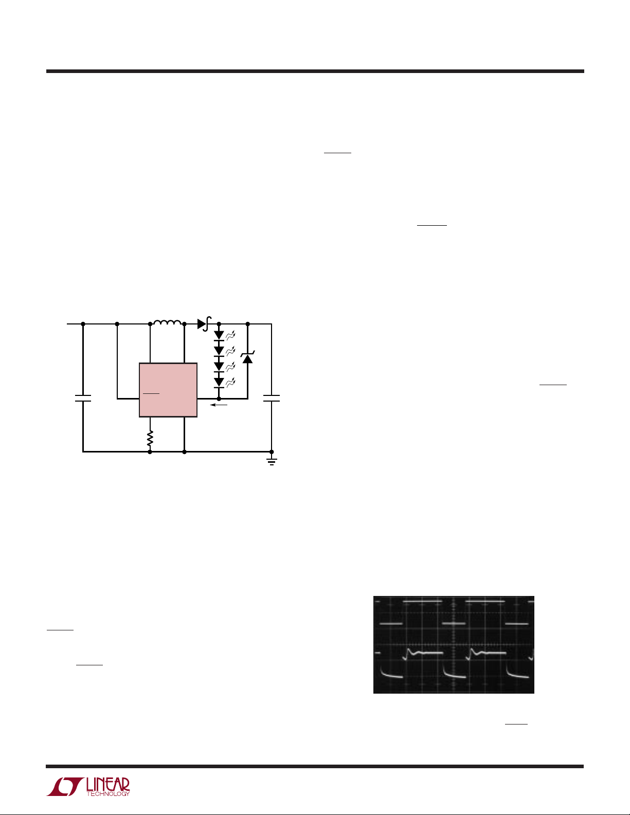
Open-Circuit Protection
For applications where the string of LEDs can be disconnected or could potentially become an open circuit, a zener
diode can be added across the LEDs to protect the LT1932
(see Figure 4). If the device is turned on without the LEDs
present, no current feedback signal is provided to the LED
pin. The LT1932 will then switch at its maximum duty
cycle, generating an output voltage 10 to 15 times greater
than the input voltage. Without the zener, the SW pin could
see more than 36V and exceed its maximum rating. The
zener voltage should be larger than the maximum forward
voltage of the LED string.
L1
V
IN
C1
4.7µF
Figure 4. LED Driver with Open-Circuit Protection
6.8µH
61
V
IN
LT1932
SHDN
R
SET
4
R
SET
1.50k
SW
LED
GND
D1
24V
35
15mA
2
C2
1µF
1932 F04
Dimming Using a PWM Signal
PWM brightness control provides the widest dimming
range (greater than 20:1) by pulsing the LEDs on and off
using the control signal. The LEDs operate at either zero or
full current, but their average current changes with the
PWM signal duty cycle. Typically, a 5kHz to 40kHz PWM
signal is used. PWM dimming with the LT1932 can be
accomplished two different ways (see Figure 6). The
SHDN pin can be driven directly or a resistor can be added
to drive the R
SET
pin.
If the SHDN pin is used, increasing the duty cycle will
increase the LED brightness. Using this method, the LEDs
can be dimmed and turned off completely using the same
control signal. A 0% duty cycle signal will turn off the
LT1932, reducing the total quiescent current to zero.
If the R
pin is used, increasing the duty cycle will
SET
decrease the brightness. Using this method, the LEDs are
dimmed using R
SHDN. If the R
the approximate value of R
and turned off completely using
SET
pin is used to provide PWM dimming,
SET
should be (where V
PWM
MAX
is
the “high” value of the PWM signal):
V
RR
=
PWM SET
•
MAX
.–015
1
V
In addition to providing the widest dimming range, PWM
brightness control also ensures the “purest” white LED
color over the entire dimming range. The true color of a
white LED changes with operating current, and is the
“purest” white at a specific forward current, usually 15mA
or 20mA. If the LED current is less than or more than this
value, the emitted light becomes more blue. For color
LCDs, this often results in a noticeable and undesirable
blue tint to the display.
When a PWM control signal is used to drive the SHDN pin
of the LT1932 (see Figure 6), the LEDs are turned off and
on at the PWM frequency. The current through them
alternates between full current and zero current, so the
average current changes with duty cycle. This ensures
that when the LEDs are on, they can be driven at the
appropriate current to give the purest white light. Figure
5 shows the LED current when a 5kHz PWM dimming
control signal is used with the LT1932. The LED current
waveform cleanly tracks the PWM control signal with no
delays, so the LED brightness varies linearly with the
PWM duty cycle.
V
PWM
2V/DIV
I
LED
10mA/DIV
50µs/DIV 1932 F05
Figure 5. PWM Dimming Using the SHDN Pin
1932f
7

LT1932
WUUU
APPLICATIO S I FOR ATIO
Dimming Using a Filtered PWM Signal
While the direct PWM method provides the widest dimming range and the purest white light output, it causes the
LT1932 to enter into Burst Mode® operation. This operation may be undesirable for some systems, as it may
reflect some noise to the input source at the PWM frequency. The solution is to filter the control signal by adding
a 10k resistor and a 0.1µF capacitor as shown in Figure 6,
converting the PWM to a DC level before it reaches the
R
pin. The 10k resistor minimizes the capacitance seen
SET
by the R
SET
pin.
Dimming Using a Logic Signal
For applications that need to adjust the LED brightness in
discrete steps, a logic signal can be used as shown in
Figure 6. R
sets the minimum LED current value (when
MIN
the NMOS is off):
R
=
22501•
MIN
R
sets how much the LED current is increased when
INCR
I
LED MIN
V
.
()
the NMOS is turned on:
R
INCR
=
22501•
.
I
()
LED INCREASE
V
Dimming Using a DC Voltage
For some applications, the preferred method of brightness
control uses a variable DC voltage to adjust the LED
current. As the DC voltage is increased, current flows
through R
ADJ
into R
, reducing the current flowing out
SET
of the R
R
ADJ
DC control voltage, I
by R
the DC control voltage is at V
R
Regulating LED Current when VIN > V
pin, thus reducing the LED current. Choose the
SET
value as shown below where V
is the current programmed
).
MAX
–.
MAX
–
SET
ADJ
, and I
=
22501•
LED(MAX)
LED(MIN)
is the minimum value of I
VV
II
() ()
LED MAX LED MIN
is the maximum
MAX
OUT
LED
(when
The LT1932 contains special circuitry that enables it to
regulate the LED current even when the input voltage is
higher than the output voltage. When VIN is less than V
OUT
,
the internal NPN LED switch (transistor Q2 in Figure 1) is
saturated to provide a lower power loss. When VIN is
greater than V
, the NPN LED switch comes out of
OUT
saturation to keep the LED current in regulation.
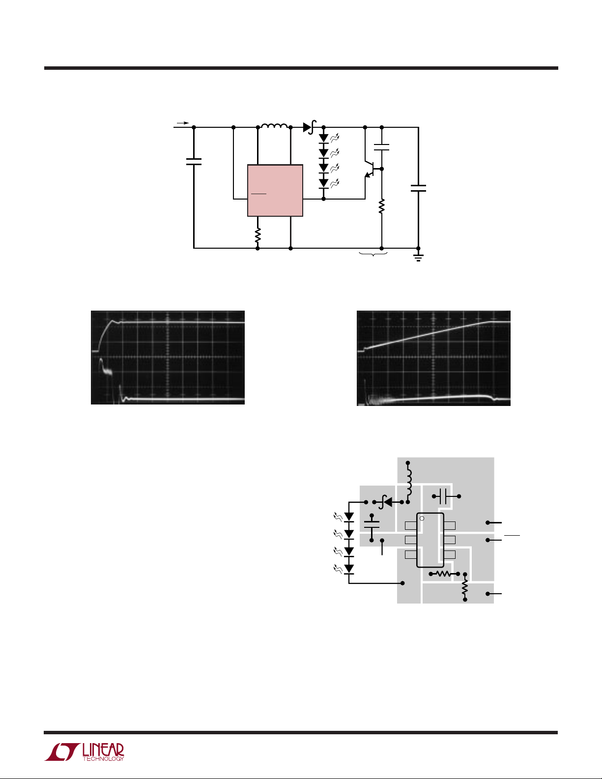
Soft-Start/Controlling Inrush Current
For many applications, it is necessary to minimize the
inrush current at start-up. When first turned on and the
LED current is zero, the LT1932 will initially command the
maximum switch current of 500mA to 600mA, which may
give an inrush current too high for some applications. A
soft-start circuit (Figure 7) can be added to significantly
reduce the start-up current spike. Figure 8 shows that
without soft-start the input current reaches almost 600mA.
Figure 9 shows that when the soft-start circuit is added,
the input current has only a brief 300mA spike, and on
average does not exceed 100mA.
8
LT1932
R
SET
PWM
Figure 6. Five Methods of LED Dimming
LT1932
R
SET
4
R
ADJ
V
DC
R
SET
1932 F06
1932f
WUUU
APPLICATIO S I FOR ATIO
LT1932
V
OUT
5V/DIV
I
200mA/DIV
I
IN
V
IN
C1
4.7µF
L1
6.8µH
61
V
SHDN
R
SET
IN
4
LT1932
R
SET
1.50k
SW
LED
GND
2
D1
Q1
2N3904
35
SOFT-START
CIRCUIT
C3
0.047µF
R1
1.5k
V
OUT
C2
1µF
1932 F07
Figure 7. Soft-Start Circuit for the LT1932
V
OUT
5V/DIV
IN
I
200mA/DIV
IN
100µs/DIV 1932 F08
Figure 8. Input Current at Start-Up Without Soft-Start
Board Layout Considerations
As with all switching regulators, careful attention must be
paid to the PCB board layout and component placement.
To maximize efficiency, switch rise and fall times are made
as short as possible. To prevent radiation and high frequency resonance problems, proper layout of the high
frequency switching path is essential. Minimize the length
and area of all traces connected to the SW pin and always
use a ground plane under the switching regulator to
minimize interplane coupling. The signal path including
the switch, output diode D1 and output capacitor C2,
contains nanosecond rise and fall times and should be
kept as short as possible. In addition, the ground connection for the R
resistor should be tied directly to the GND
SET
pin and not be shared with any other component, ensuring
a clean, noise-free connection. Recommended component placement is shown in Figure 10.
100µs/DIV 1932 F09
Figure 9. Input Current at Start-Up with Soft-Start
L1
C1
V
6
5
4
R
SET
IN
SHDN
DIMMING
CONTROL
1932 F10
C2
GND
D1
1
2
3
Figure 10. Recommended Component Placement
1932f
9

LT1932
TYPICAL APPLICATIO S
U
V
1V TO 1.5V
V
1V TO 1.5V
Single Cell Driver for One White LED
L1
IN
C1
4.7µF
2.5V PWM
DIMMING
CONTROL
C1, C2: TAIYO YUDEN JMK212BJ475 (408) 573-4150
D1: ZETEX ZHCS400 (631) 543-7100
L1: MURATA LQH3C4R7M24 (814) 237-1431
24.9k
4.7µH
61
V
SHDN
R
SET
IN
4
LT1932
R
SET
1.50k
SW
LED
GND
Single Cell Driver for Two White LEDs
L1
IN
C1
4.7µF
2.5V PWM
DIMMING
CONTROL
C1: TAIYO YUDEN JMK212BJ475 (408) 573-4150
C2: TAIYO YUDEN LMK212BJ225 (408) 573-4150
D1: ZETEX ZHCS400 (631) 543-7100
L1: MURATA LQH3C4R7M24 (814) 237-1431
24.9k
4.7µH
61
V
SHDN
R
SET
IN
4
R
1.50k
SW
LT1932
LED
GND
SET
Efficiency
D1
35
15mA
2
C2
4.7µF
1932 TA03a
80
75
70
65
EFFICIENCY (%)
60
55
50
0
VIN = 1.5V
VIN = 1.1V
510152.5 7.5 12.5
LED CURRENT (mA)
1932 TA03b
Efficiency
D1
35
15mA
2
C2
2.2µF
1932 TA04a
80
75
70
65
EFFICIENCY (%)
60
55
50
0
VIN = 1.5V
VIN = 1.1V
510152.5 7.5 12.5
LED CURRENT (mA)
1932 TA04b
10
1932f

TYPICAL APPLICATIO S
LT1932
U
1.8V TO 3V
V
1.8V TO 3V
2-Cell Driver for Two White LEDs
L1
V
IN
C1
4.7µF
2.5V DC
DIMMING
CONTROL
C1: TAIYO YUDEN JMK212BJ475 (408) 573-4150
C2: TAIYO YUDEN LMK212BJ225 (408) 573-4150
D1: ZETEX ZHCS400 (631) 543-7100
L1: MURATA LQH3C4R7M24 (814) 237-1431
60.4k
4.7µH
61
V
IN
LT1932
SHDN
R
SET
4
R
1.50k
GND
SET
2-Cell Driver for Three White LEDs Efficiency
L1
IN
C1
4.7µF
2.5V DC
DIMMING
CONTROL
C1: TAIYO YUDEN JMK212BJ475 (408) 573-4150
C2: TAIYO YUDEN EMK316BJ225 (408) 573-4150
D1: ZETEX ZHCS400 (631) 543-7100
L1: MURATA LQH3C4R7M24 (814) 237-1431
60.4k
4.7µH
61
V
SHDN
R
SET
IN
4
R
1.50k
SW
LT1932
GND
SET
SW
LED
LED
2
Efficiency
D1
35
15mA
2
D1
35
15mA
C2
2.2µF
1932 TA15a
C2
2.2µF
1932 TA06a
85
80
75
70
EFFICIENCY (%)
65
60
55
0
85
80
75
70
EFFICIENCY (%)
65
60
55
0
VIN = 3V
VIN = 1.8V
10 20515
LED CURRENT (mA)
1932 TA15b
VIN = 3V
VIN = 1.8V
5101520
LED CURRENT (mA)
1932 TA06b
1932f
11

LT1932
TYPICAL APPLICATIO S
2-Cell Driver for Four White LEDs Efficiency
U
1.8V TO 3V
V
IN
2V TO 3V
L1
V
IN
C1
4.7µF
PWM
DIMMING
CONTROL
C1: TAIYO YUDEN JMK212BJ475 (408) 573-4150
C2: TAIYO YUDEN EMK212BJ105 (408) 573-4150
D1: ZETEX ZHCS400 (631) 543-7100
L1: MURATA LQH3C4R7M24 (814) 237-1431
4.7µH
61
V
IN
LT1932
SHDN
R
SET
4
R
1.50k
GND
SET
2-Cell Driver for Five White LEDs
L1
4.7µH
SW
LED
D1
35
15mA
2
C2
1µF
1932 TA07a
85
80
75
70
EFFICIENCY (%)
65
60
55
0
VIN = 3V
VIN = 1.8V
5101520
LED CURRENT (mA)
1932 TA07b
Efficiency
D1
85
80
C1
4.7µF
PWM
DIMMING
CONTROL
C1: TAIYO YUDEN JMK212BJ475 (408) 573-4150
C2: TAIYO YUDEN TMK316BJ105 (408) 573-4150
D1: ZETEX ZHCS400 (631) 543-7100
L1: MURATA LQH3C4R7M24 (814) 237-1431
61
V
SHDN
R
IN
SET
LT1932
4
R
SET
1.50k
SW
LED
GND
2
35
15mA
C2
1µF
1932 TA05a
75
70
EFFICIENCY (%)
65
60
55
0
VIN = 3V
VIN = 2V
5101520
LED CURRENT (mA)
1932 TA05b
1932f
12

TYPICAL APPLICATIO S
Li-Ion Driver for Two White LEDs Efficiency
L1
V
2.7V TO 4.2V
IN
C1
4.7µF
3.3V PWM
DIMMING
CONTROL
C1: TAIYO YUDEN JMK212BJ475 (408) 573-4150
C2: TAIYO YUDEN LMK212BJ225 (408) 573-4150
D1: ZETEX ZHCS400 (631) 543-7100
L1: PANASONIC ELJEA6R8 (714) 373-7334
31.6k
6.8µH
61
V
SHDN
R
SET
IN
4
LT1932
R
SET
1.50k
SW
LED
GND
2
U
LT1932
D1
35
15mA
C2
2.2µF
1932 TA08a
85
80
75
70
EFFICIENCY (%)
65
60
55
0
VIN = 4.2V
VIN = 2.7V
5101520
LED CURRENT (mA)
1932 TA08b
V
2.7V TO 4.2V
Li-Ion Driver for Three White LEDs Efficiency
L1
IN
C1
4.7µF
3.3V PWM
DIMMING
CONTROL
C1: TAIYO YUDEN JMK212BJ475 (408) 573-4150
C2: TAIYO YUDEN EMK316BJ225 (408) 573-4150
D1: ZETEX ZHCS400 (631) 543-7100
L1: PANASONIC ELJEA6R8 (714) 373-7334
31.6k
6.8µH
61
V
SHDN
R
SET
IN
4
LT1932
R
SET
1.50k
SW
LED
GND
D1
35
15mA
2
C2
2.2µF
1932 TA09a
85
80
75
70
EFFICIENCY (%)
65
60
55
0
VIN = 4.2V
VIN = 2.7V
5101520
LED CURRENT (mA)
1932 TA09b
1932f
13
LT1932
TYPICAL APPLICATIO S
Li-Ion Driver for Four White LEDs Efficiency
L1
V
2.7V TO 4.2V
IN
6.8µH
U
D1
85
80
VIN = 4.2V
V
2.7V TO 4.2V
C1
4.7µF
PWM
DIMMING
CONTROL
C1: TAIYO YUDEN JMK212BJ475 (408) 573-4150
C2: TAIYO YUDEN EMK212BJ105 (408) 573-4150
D1: ZETEX ZHCS400 (631) 543-7100
L1: PANASONIC ELJEA6R8 (714) 373-7334
61
V
SHDN
R
SET
IN
4
LT1932
R
SET
1.50k
SW
LED
GND
Li-Ion Driver for Five White LEDs Efficiency
L1
IN
C1
4.7µF
PWM
DIMMING
CONTROL
C1: TAIYO YUDEN JMK212BJ475 (408) 573-4150
C2: TAIYO YUDEN TMK316BJ105 (408) 573-4150
D1: ZETEX ZHCS400 (631) 543-7100
L1: MURATA LQH3C4R7M24 (814) 237-1431
4.7µH
61
V
SHDN
R
SET
IN
4
LT1932
R
SET
1.50k
SW
LED
GND
75
70
35
15mA
2
D1
35
2
15mA
C2
1µF
1932 TA10a
C2
1µF
1932 TA11a
EFFICIENCY (%)
65
60
55
0
85
80
75
70
EFFICIENCY (%)
65
60
55
0
5101520
LED CURRENT (mA)
5101520
LED CURRENT (mA)
VIN = 2.7V
1932 TA10b
VIN = 4.2V
VIN = 2.7V
1932 TA11b
14
1932f

TYPICAL APPLICATIO S
Li-Ion Driver for Eight White LEDs Efficiency
LT1932
U
L1
V
3V TO 4.2V
IN
C1
4.7µF
3.3V DC
DIMMING
CONTROL
C1: TAIYO YUDEN JMK212BJ475 (408) 573-4150
C2: TAIYO YUDEN GMK316BJ105 (408) 573-4150
D1: ZETEX ZHCS400 (631) 543-7100
L1: MURATA LQH3C4R7M24 (814) 237-1431
80.6k
4.7µH
61
V
SHDN
R
IN
SET
LT1932
4
R
1.50k
SW
LED
GND
2
SET
PACKAGE DESCRIPTIO
D1
35
15mA
C2
1µF
1932 TA13a
85
80
75
70
EFFICIENCY (%)
65
60
55
0
VIN = 4.2V
VIN = 3V
5101520
LED CURRENT (mA)
1932 TA13b
U
S6 Package
6-Lead Plastic SOT-23
(LTC DWG # 05-08-1634)
(LTC DWG # 05-08-1636)
.20
(.008)
DATUM ‘A’
L
NOTE:
1. CONTROLLING DIMENSION: MILLIMETERS
2. DIMENSIONS ARE IN
3. DRAWING NOT TO SCALE
4. DIMENSIONS ARE INCLUSIVE OF PLATING
5. DIMENSIONS ARE EXCLUSIVE OF MOLD FLASH AND METAL BURR
6. MOLD FLASH SHALL NOT EXCEED .254mm
7. PACKAGE EIAJ REFERENCE IS:
SC-74A (EIAJ) FOR ORIGINAL
JEDEL MO-193 FOR THIN
MILLIMETERS
(INCHES)
.09 – .20
(.004 – .008)
(NOTE 2)
Information furnished by Linear Technology Corporation is believed to be accurate and reliable.
However, no responsibility is assumed for its use. Linear Technology Corporation makes no representation that the interconnection of its circuits as described herein will not infringe on existing patent rights.
2.80 – 3.10
(.110 – .118)
(NOTE 3)
A2
A
1.90
(.074)
REF
A
A1
A2
L
SOT-23
(Original)
.90 – 1.45
(.035 – .057)
.00 – 0.15
(.00 – .006)
.90 – 1.30
(.035 – .051)
.35 – .55
(.014 – .021)
SOT-23
(ThinSOT)
1.00 MAX
(.039 MAX)
.01 – .10
(.0004 – .004)
.80 – .90
(.031 – .035)
.30 – .50 REF
(.012 – .019 REF)
A1
2.60 – 3.00
(.102 – .118)
1.50 – 1.75
(.059 – .069)
(NOTE 3)
.95
(.037)
REF
PIN ONE ID
.25 – .50
(.010 – .020)
(6PLCS, NOTE 2)
S6 SOT-23 0401
1932f
15

LT1932
TYPICAL APPLICATIO
Li-Ion Driver for Ten White LEDs Efficiency
U
V
2.7V TO 4.2V
V
2.7V TO 4.2V
L1
IN
C1
4.7µF
C1: TAIYO YUDEN JMK212BJ475 (408) 573-4150
C2: TAIYO YUDEN TMK325BJ475 (408) 573-4150
D1: ZETEX ZHCS400 (631) 543-7100
L1: MURATA LQH3C100M24 (814) 237-1431
IN
C1
4.7µF
3.3V DC
DIMMING
CONTROL
C1: TAIYO YUDEN JMK212BJ475 (408) 573-4150
C2: TAIYO YUDEN TMK316BJ105 (408) 573-4150
D1: ZETEX ZHCS400 (631) 543-7100
L1: MURATA LQH3C4R7M24 (814) 237-1431
80.6k
10µH
61
V
IN
LT1932
5
SHDN
R
SET
4
R
SET
750Ω
L1
4.7µH
61
V
IN
LT1932
SHDN
R
SET
4
R
SET
1.50k
SW
LED
GND
SW
LED
GND
D1
3
2
100Ω
30mA
100Ω
C2
4.7µF
1932 TA16a
80
75
70
65
EFFICIENCY (%)
60
55
50
0
VIN = 4.2V
VIN = 2.7V
10 20 3051525
TOTAL LED CURRENT (mA)
1932 TA16b
EfficiencyLi-Ion Driver for Six White LEDs
D1
35
2
15mA
C2
1µF
1932 TA12a
85
80
75
70
EFFICIENCY (%)
65
60
55
0
VIN = 4.2V
VIN = 2.7V
5101520
LED CURRENT (mA)
1932 TA12b
RELATED PARTS
PART NUMBER DESCRIPTION COMMENTS
LT1615 Micropower DC/DC Converter in 5-Lead ThinSOT 20V at 12mA from 2.5V Input, ThinSOT Package
LT1617 Micropower Inverting DC/DC Converter in 5-Lead ThinSOT –15V at 12mA from 2.5V Input, ThinSOT Package
LT1618 Constant-Current/Constant-Voltage DC/DC Converter Drives 20 White LEDs from Li-Ion, MS10 Package
LTC1682 Doubler Charge Pump with Low Noise Linear Regulator 3.3V and 5V Outputs with 60µV
LT1930 1.4MHz Switching Regulator in 5-Lead ThinSOT 5V at 480mA from 3.3V Input, ThinSOT Package
LT1931 Inverting 1.2MHz Switching Regulator in 5-Lead ThinSOT –5V at 350mA from 5V Input, ThinSOT Package
LTC3200 Low Noise Regulated Charge Pump 5V Output with Up to 100mA Output
LTC3201 Ultralow Noise, Charge Pump 100mA, Integrated LP Filter, MSOP8
LTC3202 High Efficiency, Fractional Charge Pump 125mA, Integrated 2-Bit DAC
Linear Technology Corporation
16
1630 McCarthy Blvd., Milpitas, CA 95035-7417
(408) 432-1900 ● FAX: (408) 434-0507
●
www.linear.com
Noise, Up to 80mA Output
RMS
LT/TP 1201 2K • PRINTED IN USA
LINEAR TECHNOLOGY CORPORATION 2001
1932f
 Loading...