

Linear Technology LT1761ES5-2.5, LT1761ES5-2, LT1761ES5-1.8, LT1761ES5-5, LT1761ES5-3.3 Datasheet
...
FEATURES
■
Tiny 5-Lead SOT-23 Package
■
Low Noise: 20µV
■
Low Quiescent Current: 20µA
■
Wide Input Voltage Range: 1.8V to 20V
■
Output Current: 100mA
■
Very Low Shutdown Current: < 0.1µA
■
Low Dropout Voltage: 300mV at 100mA
■
Fixed Output Voltages: 1.5V, 1.8V, 2V, 2.5V, 2.8V,
(10Hz to 100kHz)
RMS
3V, 3.3V, 5V
■
Adjustable Output from 1.22V to 20V
■
Stable with 1µF Output Capacitor
■
Stable with Aluminum, Tantalum or
Ceramic Capacitors
■
Reverse Battery Protected
■
No Reverse Current
■
No Protection Diodes Needed
■
Overcurrent and Overtemperature Protected
U
APPLICATIO S
■
Cellular Phones
■
Pagers
■
Battery-Powered Systems
■
Frequency Synthesizers
■
Wireless Modems
LT1761 Series
100mA, Low Noise,
LDO Micropower
Regulators in SOT-23
U
DESCRIPTIO
The LT®1761 series are micropower, low noise, low
dropout regulators. With an external 0.01µF bypass
capacitor, output noise drops to 20µV
100kHz bandwidth. Designed for use in battery-powered
systems, the low 20µA quiescent current makes them an
ideal choice. In shutdown, quiescent current drops to less
than 0.1µA. The devices are capable of operating over an
input voltage from 1.8V to 20V, and can supply 100mA of
output current with a dropout voltage of 300mV. Quiescent current is well controlled, not rising in dropout as it
does with many other regulators.
The LT1761 regulators are stable with output capacitors
as low as 1µF. Small ceramic capacitors can be used
without the series resistance required by other regulators.
Internal protection circuitry includes reverse battery protection, current limiting, thermal limiting and reverse
current protection. The device is available in fixed output
voltages of 1.5V, 1.8V, 2V, 2.5V, 2.8V, 3V, 3.3V and 5V,
and as an adjustable device with a 1.22V reference voltage.
The LT1761 regulators are available in the 5-lead SOT-23
package.
, LTC and LT are registered trademarks of Linear Technology Corporation.
over a 10Hz to
RMS
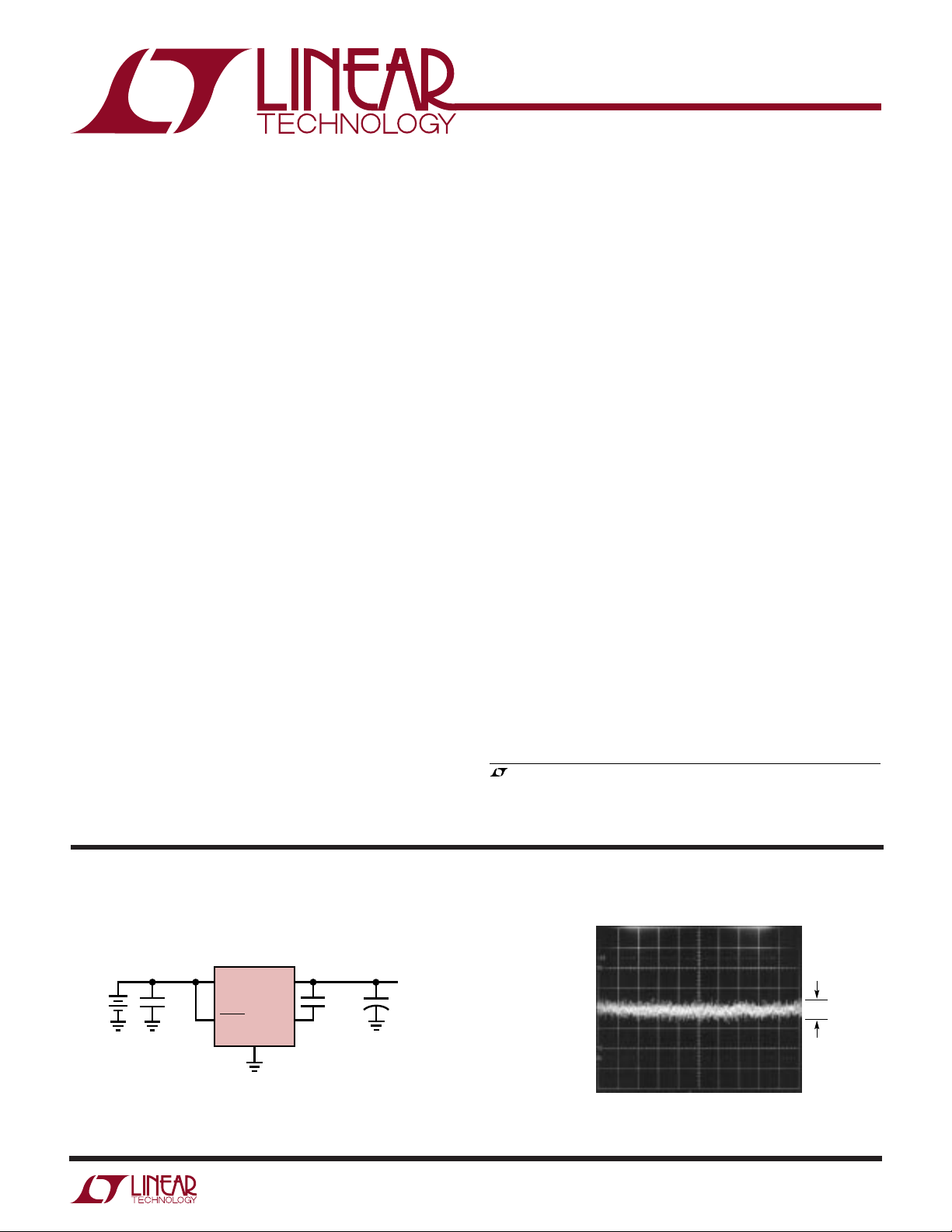
TYPICAL APPLICATIO
5V Low Noise Regulator
V
5.4V TO
20V
IN
1µF
IN
SHDN
OUT
LT1761-5
BYP
GND
U
0.01µF
+
5V AT100mA
20µV
10µF
RMS
NOISE
1761 TA01
V
OUT
100µV/DIV
10Hz to 100kHz Output Noise
1761 G48
20µV
RMS
1
LT1761 Series
WWWU
ABSOLUTE AXI U RATI GS
(Note 1)
IN Pin Voltage........................................................ ±20V
OUT Pin Voltage .................................................... ±20V
Input to Output Differential Voltage ....................... ±20V
ADJ Pin Voltage ...................................................... ±7V
BYP Pin Voltage....................................................±0.6V
SHDN Pin Voltage................................................. ±20V
UU
W
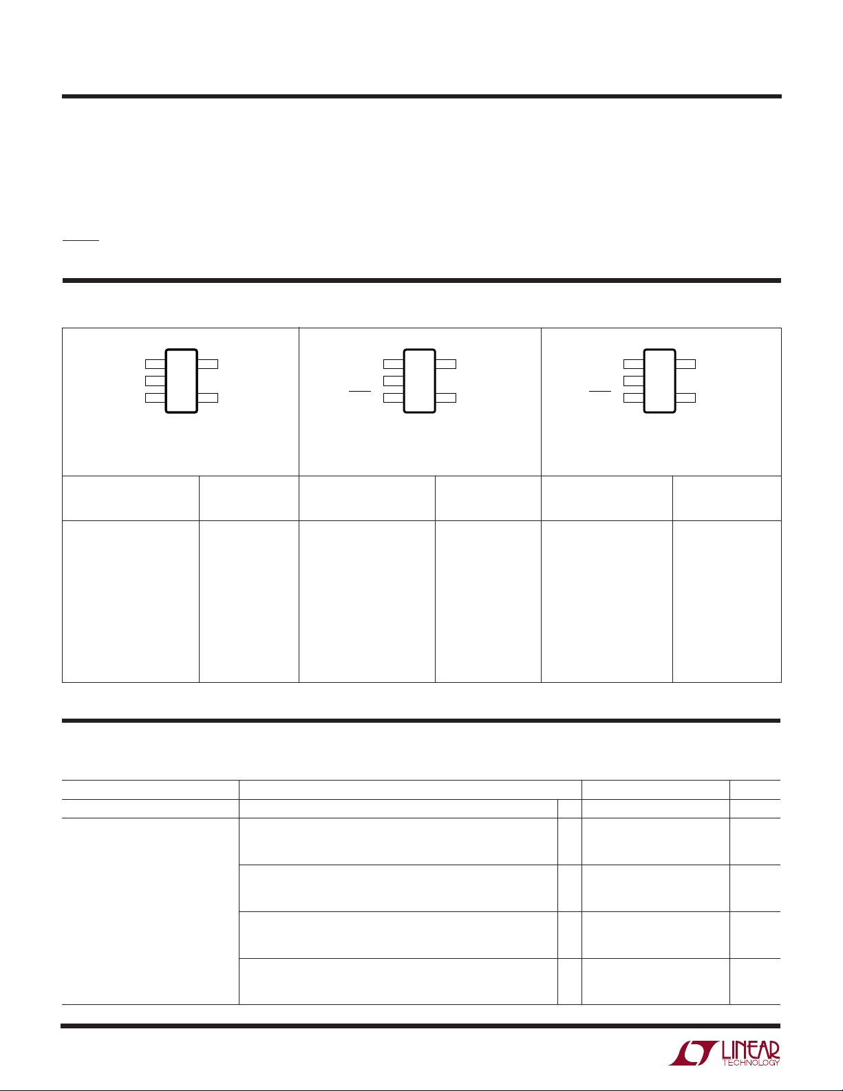
PACKAGE/ORDER I FOR ATIO
TOP VIEW
TOP VIEW
5 OUT
IN 1
IN 1
GND 2
GND 2
BYP 3
BYP 3
S5 PACKAGE
S5 PACKAGE
5-LEAD PLASTIC SOT-23
5-LEAD PLASTIC SOT-23
T
= 150°C, θJA = 250°C/W
JMAX
SEE THE APPLICATIONS INFORMATION SECTION.
ORDER PART
NUMBER
LT1761ES5-BYP
5 OUT
4 ADJ
4 ADJ
S5 PART
MARKING
LTGC LTGH LT1761ES5-1.5
LT1761ES5-SD
IN 1
GND 2
SHDN 3
S5 PACKAGE
5-LEAD PLASTIC SOT-23
T
= 150°C, θJA = 250°C/W
JMAX
SEE THE APPLICATIONS INFORMATION SECTION.
ORDER PART
NUMBER
Output Short-Circut Duration.......................... Indefinite
Operating Junction Temperature Range
(Note 2) ............................................ –40°C to 125°C
Storage Temperature Range ................. –65°C to 150°C
Lead Temperature (Soldering, 10 sec).................. 300°C
TOP VIEW
5 OUT
4 ADJ
S5 PART
MARKING
GND 2
SHDN 3
SEE THE APPLICATIONS INFORMATION SECTION.
ORDER PART
NUMBER
TOP VIEW
IN 1
S5 PACKAGE
5-LEAD PLASTIC SOT-23
T
= 150°C, θJA = 250°C/W
JMAX
5 OUT
4 BYP
S5 PART
MARKING
LT1761ES5-1.8
LT1761ES5-2
LT1761ES5-2.5
LT1761ES5-2.8
LT1761ES5-3
LT1761ES5-3.3
LT1761ES5-5
LTMT
LTJM
LTJE
LTGD
LTLB
LTGE
LTGF
LTGG
Consult factory for parts specified with wider operating temperature ranges.
ELECTRICAL CHARACTERISTICS
The ● denotes specifications which apply over the full operating temperature range, otherwise specifications are TA = 25°C. (Note 2)
PARAMETER CONDITIONS MIN TYP MAX UNITS
Minimum Input Voltage (Notes 3, 11) I
Regulated Output Voltage LT1761-1.5 VIN = 2V, I
(Note 4) 2.5V < V
= 100mA ● 1.8 2.3 V
LOAD
= 1mA 1.478 1.5 1.522 V
LOAD
IN
2.5V < V
IN
LT1761-1.8 VIN = 2.3V, I
LT1761-2 VIN = 2.5V, I
LT1761-2.5 VIN = 3V, I
2.8V < V
IN
2.8V < V
IN
< 20V, 1mA < I
3V < V
IN
3V < VIN < 20V, 1mA < I
3.5V < V
IN
3.5V < VIN < 20V, 1mA < I
< 20V, 1mA < I
< 20V, 1mA < I
= 1mA 1.775 1.8 1.825 V
LOAD
< 20V, 1mA < I
< 20V, 1mA < I
= 1mA 1.970 2 2.030 V
LOAD
= 1mA 2.465 2.5 2.535 V
LOAD
< 20V, 1mA < I
< 50mA ● 1.457 1.5 1.538 V
LOAD
< 100mA ● 1.436 1.5 1.555 V
LOAD
< 50mA ● 1.750 1.8 1.845 V
LOAD
< 100mA ● 1.725 1.8 1.860 V
LOAD
< 50mA ● 1.945 2 2.045 V
LOAD
< 100mA ● 1.920 2 2.060 V
LOAD
< 50mA ● 2.435 2.5 2.565 V
LOAD
< 100mA ● 2.415 2.5 2.575 V
LOAD
2
LT1761 Series
ELECTRICAL CHARACTERISTICS
The ● denotes specifications which apply over the full operating temperature range, otherwise specifications are TA = 25°C. (Note 2)
PARAMETER CONDITIONS MIN TYP MAX UNITS
Regulated Output Voltage LT1761-2.8 VIN = 3.3V, I
(Note 4) 3.8V < V
3.8V < V
LT1761-3 VIN = 3.5V, I
4V < V
IN
4V < VIN < 20V, 1mA < I
LT1761-3.3 VIN = 3.8V, I
4.3V < V
4.3V < V
LT1761-5 VIN = 5.5V, I
6V < V
IN
6V < V
IN
ADJ Pin Voltage LT1761 VIN = 2V, I
(Note 3, 4) 2.3V < V
2.3V < V
Line Regulation LT1761-1.5 ∆VIN = 2V to 20V, I
LT1761-1.8 ∆V
LT1761-2 ∆V
LT1761-2.5 ∆V
LT1761-2.8 ∆V
LT1761-3 ∆V
LT1761-3.3 ∆V
LT1761-5 ∆V
LT1761(Note 3) ∆V
= 2.3V to 20V, I
IN
= 2.5V to 20V, I
IN
= 3V to 20V, I
IN
= 3.3V to 20V, I
IN
= 3.5V to 20V, I
IN
= 3.8V to 20V, I
IN
= 5.5V to 20V, I
IN
= 2V to 20V, I
IN
Load Regulation LT1761-1.5 VIN = 2.5V, ∆I
V
= 2.5V, ∆I
IN
= 2.5V, ∆I
V
IN
= 2.5V, ∆I
V
IN
LT1761-1.8 VIN = 2.8V, ∆I
V
= 2.8V, ∆I
IN
= 2.8V, ∆I
V
IN
= 2.8V, ∆I
V
IN
LT1761-2 VIN = 3V, ∆I
= 3V, ∆I
V
IN
V
= 3V, ∆I
IN
= 3V, ∆I
V
IN
LT1761-2.5 VIN = 3.5V, ∆I
= 3.5V, ∆I
V
IN
V
= 3.5V, ∆I
IN
= 3.5V, ∆I
V
IN
LT1761-2.8 VIN = 3.8V, ∆I
= 3.8V, ∆I
V
IN
V
= 3.8V, ∆I
IN
= 3.8V, ∆I
V
IN
LT1761-3 VIN = 4V, ∆I
= 4V, ∆I
V
IN
V
= 4V, ∆I
IN
= 4V, ∆I
V
IN
= 1mA 2.762 2.8 2.838 V
LOAD
< 20V, 1mA < I
IN
< 20V, 1mA < I
IN
= 1mA 2.960 3 3.040 V
LOAD
< 20V, 1mA < I
= 1mA 3.250 3.3 3.350 V
LOAD
< 20V, 1mA < I
IN
< 20V, 1mA < I
IN
= 1mA 4.935 5 5.065 V
LOAD
< 20V, 1mA < I
< 20V, 1mA < I
= 1mA 1.205 1.220 1.235 V
LOAD
< 20V, 1mA < I
IN
< 20V, 1mA < I
IN
LOAD
LOAD
LOAD
LOAD
LOAD
LOAD
LOAD
LOAD
LOAD
= 1mA to 50mA 10 20 mV
LOAD
= 1mA to 50mA ● 35 mV
LOAD
= 1mA to 100mA 14 30 mV
LOAD
= 1mA to 100mA ● 55 mV
LOAD
= 1mA to 50mA 10 20 mV
LOAD
= 1mA to 50mA ● 35 mV
LOAD
= 1mA to 100mA 15 30 mV
LOAD
= 1mA to 100mA ● 60 mV
LOAD
= 1mA to 50mA 10 20 mV
LOAD
= 1mA to 50mA ● 35 mV
LOAD
= 1mA to 100mA 15 35 mV
LOAD
= 1mA to 100mA ● 65 mV
LOAD
= 1mA to 50mA 10 20 mV
LOAD
= 1mA to 50mA ● 35 mV
LOAD
= 1mA to 100mA 20 40 mV
LOAD
= 1mA to 100mA ● 80 mV
LOAD
= 1mA to 50mA 10 20 mV
LOAD
= 1mA to 50mA ● 38 mV
LOAD
= 1mA to 100mA 20 40 mV
LOAD
= 1mA to 100mA ● 86 mV
LOAD
= 1mA to 50mA 10 20 mV
LOAD
= 1mA to 50mA ● 40 mV
LOAD
= 1mA to 100mA 20 40 mV
LOAD
= 1mA to 100mA ● 90 mV
LOAD
< 50mA ● 2.732 2.8 2.868 V
LOAD
< 100mA ● 2.706 2.8 2.884 V
LOAD
< 50mA ● 2.930 3 3.070 V
LOAD
< 100mA ● 2.900 3 3.090 V
LOAD
< 50mA ● 3.230 3.3 3.370 V
LOAD
< 100mA ● 3.190 3.3 3.400 V
LOAD
< 50mA ● 4.900 5 5.100 V
LOAD
< 100mA ● 4.850 5 5.120 V
LOAD
< 50mA ● 1.190 1.220 1.250 V
LOAD
< 100mA ● 1.170 1.220 1.260 V
LOAD
= 1mA ● 110 mV
= 1mA ● 110 mV
= 1mA ● 110 mV
= 1mA ● 110 mV
= 1mA ● 110 mV
= 1mA ● 110 mV
= 1mA ● 110 mV
= 1mA ● 110 mV
= 1mA ● 110 mV
3
LT1761 Series
ELECTRICAL CHARACTERISTICS
The ● denotes specifications which apply over the full operating temperature range, otherwise specifications are TA = 25°C. (Note 2)
PARAMETER CONDITIONS MIN TYP MAX UNITS
Load Regulation LT1761-3.3 VIN = 4.3V, ∆I
VIN = 4.3V, ∆I
V
= 4.3V, ∆I
IN
VIN = 4.3V, ∆I
LT1761-5 VIN = 6V, ∆I
V
= 6V, ∆I
IN
VIN = 6V, ∆I
V
= 6V, ∆I
IN
LT1761 (Note 3) VIN = 2.3V, ∆I
V
= 2.3V, ∆I
IN
VIN = 2.3V, ∆I
V
= 2.3V, ∆I
IN
Dropout Voltage I
VIN = V
OUT(NOMINAL)
(Notes 5, 6, 11) I
GND Pin Current I
V
= V
IN
OUT(NOMINAL)
(Notes 5, 7) I
Output Voltage Noise C
= 1mA 0.10 0.15 V
LOAD
I
= 1mA ● 0.19 V
LOAD
= 10mA 0.17 0.22 V
LOAD
I
= 10mA ● 0.29 V
LOAD
I
= 50mA 0.24 0.28 V
LOAD
I
= 50mA ● 0.38 V
LOAD
I
= 100mA 0.30 0.35 V
LOAD
I
= 100mA ● 0.45 V
LOAD
= 0mA ● 20 45 µA
LOAD
I
= 1mA ● 55 100 µA
LOAD
= 10mA ● 230 400 µA
LOAD
I
= 50mA ● 12 mA
LOAD
I
= 100mA ● 2.2 4 mA
LOAD
= 10µF, C
OUT
= 0.01µF, I
BYP
ADJ Pin Bias Current (Notes 3, 8) 30 100 nA
Shutdown Threshold V
SHDN Pin Current V
(Note 9) V
Quiescent Current in Shutdown VIN = 6V, V
Ripple Rejection (Note 3) VIN – V
Current Limit VIN = 7V, V
Input Reverse Leakage Current VIN = –20V, V
Reverse Output Current LT1761-1.5 V
(Note 10) LT1761-1.8 V
= Off to On ● 0.8 2 V
OUT
V
= On to Off ● 0.25 0.65 V
OUT
= 0V ● 0 0.5 µA
SHDN
= 20V ● 13 µA
SHDN
= 0V 0.01 0.1 µA
SHDN
= 1.5V (Avg), V
OUT
I
= 50mA
LOAD
= 0V 200 mA
= V
OUT(NOMINAL)
OUT
+ 1V, ∆V
= 0V ● 1mA
OUT
= 1.5V, VIN < 1.5V 10 20 µA
OUT
= 1.8V, VIN < 1.8V 10 20 µA
OUT
= 2V, VIN < 2V 10 20 µA
OUT
= 2.5V, VIN < 2.5V 10 20 µA
OUT
= 2.8V, VIN < 2.8V 10 20 µA
OUT
= 3V, VIN < 3V 10 20 µA
OUT
= 3.3V, VIN < 3.3V 10 20 µA
OUT
= 5V, VIN < 5V 10 20 µA
OUT
= 1.22V, VIN < 1.22V 5 10 µA
OUT
V
IN
LT1761-2 V
LT1761-2.5 V
LT1761-2.8 V
LT1761-3 V
LT1761-3.3 V
LT1761-5 V
LT1761 (Note 3) V
= 1mA to 50mA 10 20 mV
LOAD
= 1mA to 50mA ● 40 mV
LOAD
= 1mA to 100mA 20 40 mV
LOAD
= 1mA to 100mA ● 100 mV
LOAD
= 1mA to 50mA 15 30 mV
LOAD
= 1mA to 50mA ● 60 mV
LOAD
= 1mA to 100mA 25 65 mV
LOAD
= 1mA to 100mA ● 150 mV
LOAD
= 1mA to 50mA 1 6 mV
LOAD
= 1mA to 50mA ● 12 mV
LOAD
= 1mA to 100mA 1 12 mV
LOAD
= 1mA to 100mA ● 50 mV
LOAD
= 100mA, BW = 10Hz to 100kHz 20 µV
LOAD
= 0.5V
RIPPLE
= –5% ● 110 mA
OUT
P-P
, f
= 120Hz, 55 65 dB
RIPPLE
RMS
Note 1: Absolute Maximum Ratings are those values beyond which the life
of a device may be impaired.
Note 2: The LT1761 regulators are tested and specified under pulse load
conditions such that T
≈ TA. The LT1761 is 100% production tested at
J
4
TA = 25°C. Performance at –40°C and 125°C is assured by design,
characterization and correlation with statistical process controls.
Note 3: The LT1761 (adjustable versions) are tested and specified for
these conditions with the ADJ pin connected to the OUT pin.
TEMPERATURE (°C)
–50
OUTPUT VOLTAGE (V)
100
1761 G06
050
1.84
1.83
1.82
1.81
1.80
1.79
1.78
1.77
1.76
–25 25 75 125
IL = 1mA
ELECTRICAL CHARACTERISTICS
LT1761 Series
Note 4: Operating conditions are limited by maximum junction
temperature. The regulated output voltage specification will not apply for
all possible combinations of input voltage and output current. When
operating at maximum input voltage, the output current range must be
limited. When operating at maximum output current, the input voltage
range must be limited.
Note 5: To satisfy requirements for minimum input voltage, the LT1761
(adjustable version) is tested and specified for these conditions with an
external resistor divider (two 250k resistors) for an output voltage of
2.44V. The external resistor divider will add a 5µA DC load on the output.
Note 6: Dropout voltage is the minimum input to output voltage differential
needed to maintain regulation at a specified output current. In dropout, the
output voltage will be equal to: V
– V
IN
DROPOUT
.
Note 7: GND pin current is tested with VIN = V
(whichever is greater) and a current source load. This means the device is
tested while operating in its dropout region or at the minimum input
voltage specification. This is the worst-case GND pin current. The GND pin
current will decrease slightly at higher input voltages.
Note 8: ADJ pin bias current flows into the ADJ pin.
Note 9: SHDN pin current flows into the SHDN pin.
Note 10: Reverse output current is tested with the IN pin grounded and the
OUT pin forced to the rated output voltage. This current flows into the OUT
pin and out the GND pin.
Note 11: For the LT1761, LT1761-1.5, LT1761-1.8 and LT1761-2 dropout
voltage will be limited by the minimum input voltage specification under
some output voltage/load conditions. See the curve of Minimum Input
Voltage in the Typical Performance Characteristics.
UW
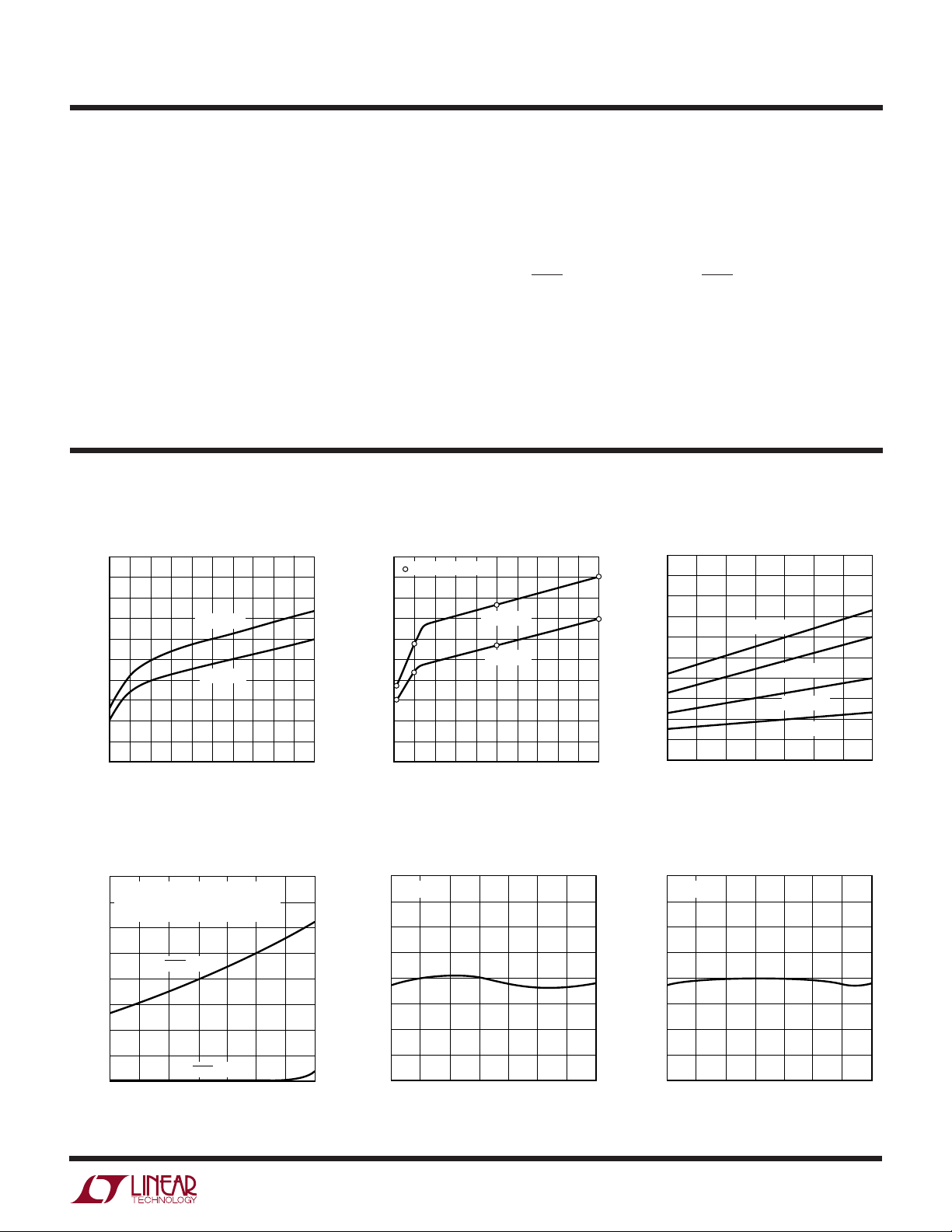
TYPICAL PERFOR A CE CHARACTERISTICS
Typical Dropout Voltage
500
450
400
350
300
250
200
150
DROPOUT VOLTAGE (mV)
100
50
0
0 102030
40
OUTPUT CURRENT (mA)
TJ = 125°C
TJ = 25°C
60 70 80 90 100
50
1761 G00
Guaranteed Dropout Voltage
500
= TEST POINTS
450
400
350
300
250
200
150
DROPOUT VOLTAGE (mV)
100
50
0
0 102030
TJ ≤ 125°C
TJ ≤ 25°C
40
50
OUTPUT CURRENT (mA)
60 70 80 90 100
1761 G01
OUT(NOMINAL)
Dropout Voltage
500
450
400
350
300
250
200
150
DROPOUT VOLTAGE (mV)
100
50
0
–50
–25
IL = 100mA
0
TEMPERATURE (°C)
or VIN = 2.3V
IL = 50mA
IL = 10mA
IL = 1mA
50
25
75
100
125
1761 G01.1
40
35
30
25
20
15
10
QUIESCENT CURRENT (µA)
5
0
–50
Quiescent Current
VIN = 6V
= ∞ (250k FOR LT1761-BYP, -SD)
R
L
= 0 (5µA FOR LT1761-BYP, -SD)
I
L
V
= V
SHDN
IN
V
= 0V
SHDN
–25 25 75 125
050
TEMPERATURE (°C)
100
1761 G03
LT1761-1.5
Output Voltage
1.528
IL = 1mA
1.521
1.514
1.507
1.500
1.493
OUTPUT VOLTAGE (V)
1.486
1.479
1.472
–25 25 75 125
–50
050
TEMPERATURE (°C)
LT1761-1.8
Output Voltage
100
1761 G51
5
 Loading...