

Linear Technology LT1721, LT1720 Datasheet
FEATURES
■
UltraFast: 4.5ns at 20mV Overdrive
7ns at 5mV Overdrive
■
Low Power: 4mA per Comparator
■
Optimized for 3V and 5V Operation
■
Pinout Optimized for High Speed Ease of Use
■
Input Voltage Range Extends 100mV
Below Negative Rail
■
TTL/CMOS Compatible Rail-to-Rail Outputs
■
Internal Hysteresis with Specified Limits
■
Low Dynamic Current Drain; 15µA/(V-MHz),
Dominated by Load In Most Circuits
U
APPLICATIO S
■
High Speed Differential Line Receiver
■
Crystal Oscillator Circuits
■
Window Comparators
■
Threshold Detectors/Discriminators
■
Pulse Stretchers
■
Zero-Crossing Detectors
■
High Speed Sampling Circuits
LT1720/LT1721
Dual/Quad,
4.5ns, Single Supply
3V/5V Comparators
with Rail-to-Rail Outputs
U
DESCRIPTIO
The LT®1720/LT1721 are UltraFastTM dual/quad comparators optimized for single supply operation, with a supply
voltage range of 2.7V to 6V. The input voltage range extends
from 100mV below ground to 1.2V below the supply voltage.
Internal hysteresis makes the LT1720/LT1721 easy to use
even with slow moving input signals. The rail-to-rail outputs
directly interface to TTL and CMOS. Alternatively, the symmetric output drive can be harnessed for analog applications
or for easy translation to other single supply logic levels.
The LT1720 is available in the 8-pin MSOP and SO packages;
three pins per comparator plus power and ground. The
LT1721 is available in the 16-pin SSOP and S packages.
The pinouts of the LT1720/LT1721 minimize parasitic effects
by placing the most sensitive inputs (inverting) away from the
outputs, shielded by the power rails. The LT1720/LT1721 are
ideal for systems where small size and low power are
paramount.
, LTC and LT are registered trademarks of Linear Technology Corporation.
UltraFast is a trademark of Linear Technology Corporation.
U
TYPICAL APPLICATIO
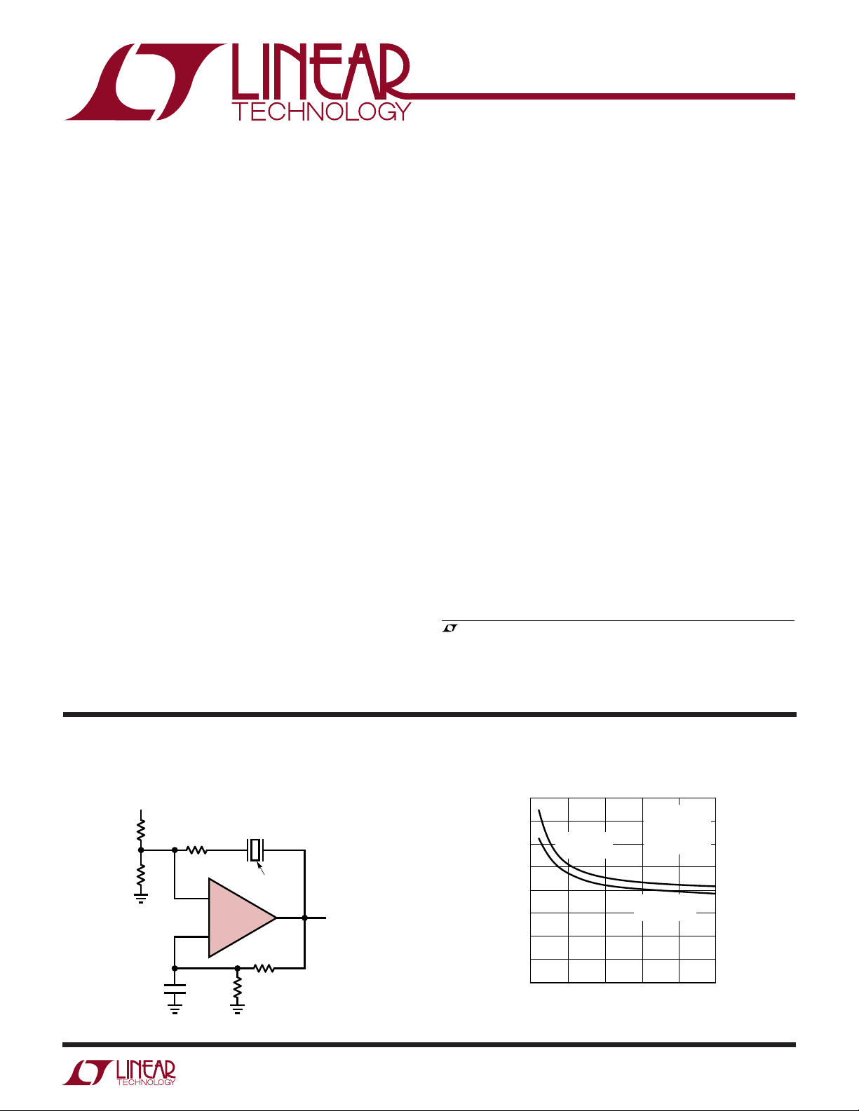
2.7V to 6V Crystal Oscillator with TTL/CMOS Output
2.7V TO 6V
2k
620Ω
1MHz TO 10MHz
CRYSTAL (AT-CUT)
220Ω
+
C1
1/2 LT1720
–
0.01µF 1.8k
GROUND
CASE
2k
1720/21 TA01
OUTPUT
Propagation Delay vs Overdrive
8
7
RISING EDGE
6
5
4
DELAY (ns)
3
2
1
0
0
)
(t
PDLH
FALLING EDGE
10 20 40
OVERDRIVE (mV)
30
25°C
V
STEP
V
CC
C
LOAD
(t
= 100mV
= 5V
PDHL
= 10pF
)
50
1720/21 TA02
1
LT1720/LT1721
WW
W
ABSOLUTE MAXIMUM RATINGS
U
(Note 1)
Supply Voltage, VCC to GND ...................................... 7V
Input Current ...................................................... ±10mA
Output Current (Continuous) ............................. ±20mA
Junction Temperature........................................... 150°C
Lead Temperature (Soldering, 10 sec)..................300°C
U
W
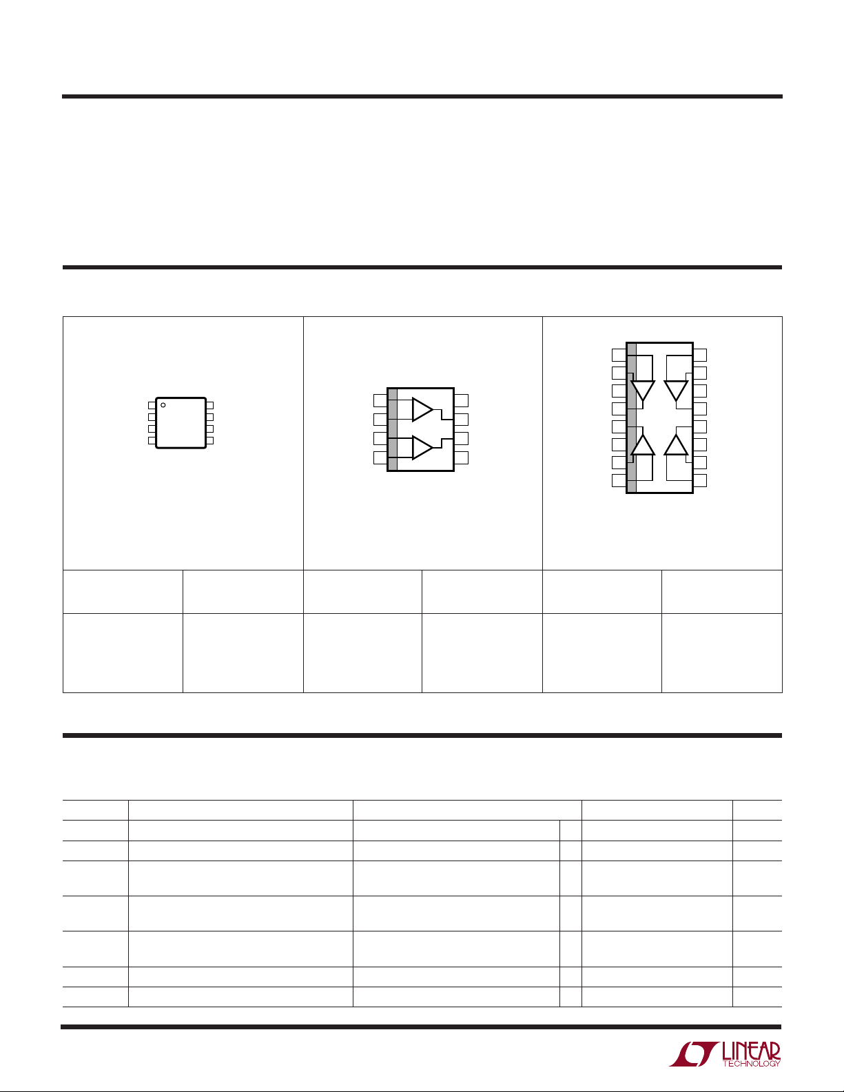
PACKAGE/ORDER INFORMATION
TOP VIEW
+IN A
1
–IN A
2
–IN B
3
+IN B
4
MS8 PACKAGE
8-LEAD PLASTIC MSOP
T
= 150°C, θJA = 230°C/W
JMAX
8
7
6
5
V
CC
OUT A
OUT B
GND
+IN A
1
–IN A
2
–IN B
3
+IN B
4
8-LEAD PLASTIC SO
T
= 150°C, θJA = 200°C/W
JMAX
S8 PACKAGE
Storage Temperature Range ................. –65°C to 150°C
Operating Temperature Range
C Grade .................................................. 0°C to 70°C
I Grade .............................................. – 40°C to 85°C
U
TOP VIEW
–IN A
TOP VIEW
1
+IN A
2
GND
8
V
CC
OUT A
7
OUT B
6
GND
5
3
OUT A
4
OUT B
5
GND
6
+IN B
7
–IN B
8
GN PACKAGE
16-LEAD NARROW
PLASTIC SSOP
T
= 150°C, θJA = 135°C/ W (GN)
JMAX
= 150°C, θJA = 115°C/ W (S)
T
JMAX
16
15
14
13
12
11
10
9
S PACKAGE
16-LEAD PLASTIC SO
–IN D
+IN D
V
CC
OUT D
OUT C
V
CC
+IN C
–IN C
ORDER PART
NUMBER
LT1720CMS8
MS8
PART MARKING
LTDS
ORDER PART
NUMBER
LT1720CS8
LT1720IS8
S8
PART MARKING
1720
1720I
ORDER PART
NUMBER
LT1721CGN
LT1721CS
GN
PART MARKING
1721
1721I
LT1721IGN
LT1721IS
Consult factory for Military grade parts.
ELECTRICAL CHARACTERISTICS
range, otherwise specifications are at TA = 25°C. VCC = 5V, VCM = 1V, C
SYMBOL PARAMETER CONDITIONS MIN TYP MAX UNITS
V
CC
V
CMR
+
V
TRIP
–
V
TRIP
V
OS
V
HYST
∆VOS/∆T Input Offset Voltage Drift ● 10 µV/°C
Supply Voltage ● 2.7 6 V
Common Mode Voltage Range (Note 2) ● –0.1 VCC – 1.2 V
Input Trip Points (Note 3) –2.0 5.5 mV
Input Trip Points (Note 3) –5.5 2.0 mV
Input Offset Voltage (Note 3) 1.0 3.0 mV
Input Hysteresis Voltage (Note 3) ● 2.0 3.5 5.0 mV
The ● denotes specifications that apply over the full operating temperature
= 10pF, V
OUT
OVERDRIVE
= 20mV, unless otherwise specified.
● –3.0 6.5 mV
● –6.5 3.0 mV
● 4.5 mV
2
LT1720/LT1721
ELECTRICAL CHARACTERISTICS
range, otherwise specifications are at TA = 25°C. VCC = 5V, VCM = 1V, C
The ● denotes specifications that apply over the full operating temperature
= 10pF, V
OUT
OVERDRIVE
= 20mV, unless otherwise specified.
SYMBOL PARAMETER CONDITIONS MIN TYP MAX UNITS
I
B
I
OS
Input Bias Current ● –6 0 µA
Input Offset Current ● 0.6 µA
CMRR Common Mode Rejection Ratio (Note 4) ● 55 70 dB
PSRR Power Supply Rejection Ratio (Note 5) ● 65 80 dB
A
V
V
OH
V
OL
I
CC
t
PD20
t
PD5
∆t
PD
t
SKEW
t
r
t
f
t
JITTER
f
MAX
Voltage Gain (Note 6) ∞
Output High Voltage I
Output Low Voltage I
= 4mA, VIN = V
SOURCE
= 10mA, VIN = V
SINK
+
+ 10mV ● VCC – 0.4 V
TRIP
–
– 10mV ● 0.4 V
TRIP
Supply Current (Per Comparator) VCC = 5V ● 47 mA
= 3V ● 3.5 6 mA
V
CC
Propagation Delay V
Propagation Delay V
OVERDRIVE
OVERDRIVE
= 20mV (Note 7) 4.5 6.5 ns
● 8.0 ns
= 5mV (Notes 7, 8) 7 10 ns
● 13 ns
Differential Propagation Delay (Note 9) Between Channels 0.3 1.0 ns
+
Propagation Delay Skew (Note 10) Between t
PD
–
/t
PD
0.5 1.5 ns
Output Rise Time 10% to 90% 2.5 ns
Output Fall Time 90% to 10% 2.2 ns
Output Timing Jitter VIN = 1.2V
VCM = 2V, f = 20MHz t
Maximum Toggle Frequency V
OVERDRIVE
V
OVERDRIVE
(6dBm), ZIN = 50Ω t
P-P
= 50mV, VCC = 3V 70.0 MHz
= 50mV, VCC = 5V 62.5 MHz
PD
PD
+
–
15 ps
11 ps
RMS
RMS
Note 1: Absolute Maximum Ratings are those values beyond which the
life of a device may be impaired.
Note 2: If one input is within these common mode limits, the other
input can go outside the common mode limits and the output will be
valid.
Note 3: The LT1720/LT1721 comparators include internal hysteresis.
The trip points are the input voltage needed to change the output state
in each direction. The offset voltage is defined as the average of V
and V
–
, while the hysteresis voltage is the difference of these two.
TRIP
TRIP
Note 4: The common mode rejection ratio is measured with VCC = 5V
and is defined as the change in offset voltage measured from V
–0.1V to V
= 3.8V, divided by 3.9V.
CM
CM
=
Note 5: The power supply rejection ratio is measured with VCM = 1V
and is defined as the change in offset voltage measured from V
2.7V to V
= 6V, divided by 3.3V.
CC
CC
=
Note 6: Because of internal hysteresis, there is no small-signal region
in which to measure gain. Proper operation of internal circuity is
ensured by measuring V
and VOL with only 10mV of overdrive.
OH
Note 7: Propagation delay measurements made with 100mV steps.
Overdrive is measured relative to V
TRIP
±
.
Note 8: tPD cannot be measured in automatic handling equipment with
low values of overdrive. The LT1720/LT1721 are 100% tested with a
100mV step and 20mV overdrive. Correlation tests have shown that
limits can be guaranteed with this test, if additional DC tests are
t
PD
performed to guarantee that all internal bias conditions are correct.
+
Note 9: Differential propagation delay is defined as the larger of the
two:
∆t
∆t
PDLH
PDHL
= t
PDLH(MAX)
= t
PDHL(MAX)
– t
PDLH(MIN)
– t
PDHL(MIN)
where (MAX) and (MIN) denote the maximum and minimum values of
a given measurement across the different comparator channels.
Note 10: Propagation Delay Skew is defined as:
t
= |t
– t
SKEW
PDLH
PDHL
|
3
LT1720/LT1721
TEMPERATURE (°C)
–50
3.6
3.8
4.2
25 75
1720/21 G03
0.2
0
–25 0
50 100 125
–0.2
–0.4
4.0
COMMON MODE INPUT VOLTAGE (V)
VCC = 5V
SUPPLY VOLTAGE (V)
0
0
SUPPLY CURRENT PER COMPARATOR (mA)
4
7
2
4
5
1720/21 G06
3
2
1
6
5
1
3
6
7
25°C
125°C
–55°C
SUPPLY VOLTAGE (V)
2.5
4.5
DELAY (ns)
5.0
4.0
4.0 5.0
1720/21 G09
3.0 3.5
4.5 5.5 6.0
RISING EDGE
(t
PDLH
)
FALLING EDGE
(t
PDHL
)
25°C
V
STEP
= 100mV
OVERDRIVE = 20mV
C
LOAD
= 10pF
W
U
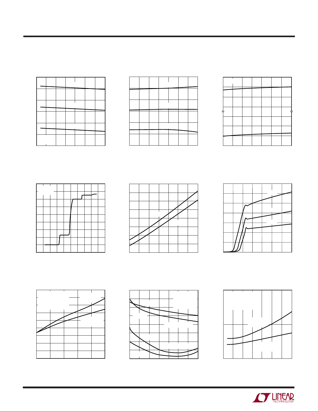
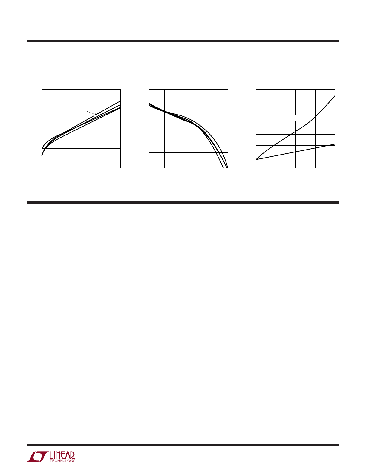
TYPICAL PERFORMANCE CHARACTERISTICS
Input Offset and Trip Voltages
vs Supply Voltage
3
V
2
1
0
–1
AND TRIP POINT VOLTAGE (mV)
–2
OS
V
25°C
V
= 1V
CM
–3
2.5
3.0 3.5
SUPPLY VOLTAGE (V)
TRIP
V
V
TRIP
4.5 5.5 6.0
4.0 5.0
Input Current
vs Differential Input Voltage
2
25°C
1
V
= 5V
CC
0
–1
–2
–3
–4
INPUT CURRENT (µA)
–5
–6
–7
–4 –3 –2 –1 0 5
–5
DIFFERENTIAL INPUT VOLTAGE (V)
+
OS
–
1720/21 G01
1234
1720/21 G04
Input Offset and Trip Voltages
vs Temperature
3
+
V
2
1
0
–1
AND TRIP POINT VOLTAGE (mV)
–2
OS
V
–3
–50 0 50 75 125
–25 25 100
TRIP
V
OS
–
V
TRIP
TEMPERATURE (°C)
1720/21 G02
Quiescent Supply Current
vs Temperature
6.0
5.5
5.0
4.5
4.0
3.5
3.0
2.5
2.0
–50
QUIESCENT SUPPLY CURRENT PER COMPARATOR (mA)
VCC = 5V
–25 0 50
25
TEMPERATURE (˚C)
= 3V
V
CC
75 100 125
1720/21 G05
Input Common Mode Limits
vs Temperature
Quiescent Supply Current
vs Supply Voltage
Propagation Delay
vs Load Capacitance
9
25°C
= 100mV
V
8
STEP
OVERDRIVE = 20mV
7
V
= 5V
CC
6
5
4
DELAY (ns)
3
2
1
0
0
4
10 20 40
OUTPUT LOAD CAPACITANCE (pF)
30
RISING EDGE
)
(t
PDLH
FALLING EDGE
)
(t
PDHL
1720/21 G07
Propagation Delay
vs Temperature
8.0
7.5
7.0
6.5
6.0
5.5
5.0
PROPAGATION DELAY (ns)
4.5
50
4.0
–50
VCC = 3V
VCC = 5V
VCC = 5V
VCC = 3V
–25 0 50
25
TEMPERATURE (°C)
t
PDLH
VCM = 1V
V
= 100mV
STEP
C
= 10pF
LOAD
OVERDRIVE = 5mV
OVERDRIVE = 20mV
75 100 125
1720/21 G08
Propagation Delay
vs Supply Voltage
W
FREQUENCY (MHz)
0
7
8
10
30
NO LOAD
1720/21 G12
6
5
10 20 40
4
3
9
SUPPLY CURRENT PER COMPARATOR (mA)
25°C
V
CC
= 5V
C
LOAD
= 20pF
U
TYPICAL PERFORMANCE CHARACTERISTICS
LT1720/LT1721
Output Low Voltage
vs Load Current
0.5
VCC = 5V
= 1V
V
CM
= –15mV
V
IN
0.4
0.3
–55°C
OUTPUT VOLTAGE (V)
0.2
0.1
4
0
OUTPUT SINK CURRENT (mA)
V
CC
8
125°C
= 2.7V
125°C
25°C
12
16
20
1720/21 G10
Output High Voltage
vs Load Current
0.0
(V)
125°C
CC
–0.2
–0.4
–0.6
–0.8
OUTPUT VOLTAGE RELATIVE TO V
–1.0
0
OUTPUT SOURCE CURRENT (mA)
UUU
PIN FUNCTIONS
LT1720
+IN A (Pin 1): Noninverting Input of Comparator A.
Supply Current vs Frequency
VCC = 5V
= 1V
V
CM
= 15mV
V
IN
–55°C
25°C
25°C
V
= 2.7V
CC
4
12
16
8
20
1720/21 G11
LT1721
–IN A (Pin 1): Inverting Input of Comparator A.
–IN A (Pin 2): Inverting Input of Comparator A.
–IN B (Pin 3): Inverting Input of Comparator B.
+IN B (Pin 4): Noninverting Input of Comparator B.
GND (Pin 5): Ground.
OUT B (Pin 6): Output of Comparator B.
OUT A (Pin 7): Output of Comparator A.
VCC (Pin 8): Positive Supply Voltage.
+IN A (Pin 2): Noninverting Input of Comparator A.
GND (Pins 3, 6): Ground.
OUT A (Pin 4): Output of Comparator A.
OUT B (Pin 5): Output of Comparator B.
+IN B (Pin 7): Noninverting Input of Comparator B.
–IN B (Pin 8): Inverting Input of Comparator B.
–IN C (Pin 9): Inverting Input of Comparator C.
+IN C (Pin 10): Noninverting Input of Comparator C.
VCC (Pins 11, 14): Positive Supply Voltage.
OUT C (Pin 12): Output of Comparator C.
OUT D (Pin 13): Output of Comparator D.
+IN D (Pin 15): Noninverting Input of Comparator D.
–IN D (Pin 16): Inverting Input of Comparator D.
5
LT1720/LT1721
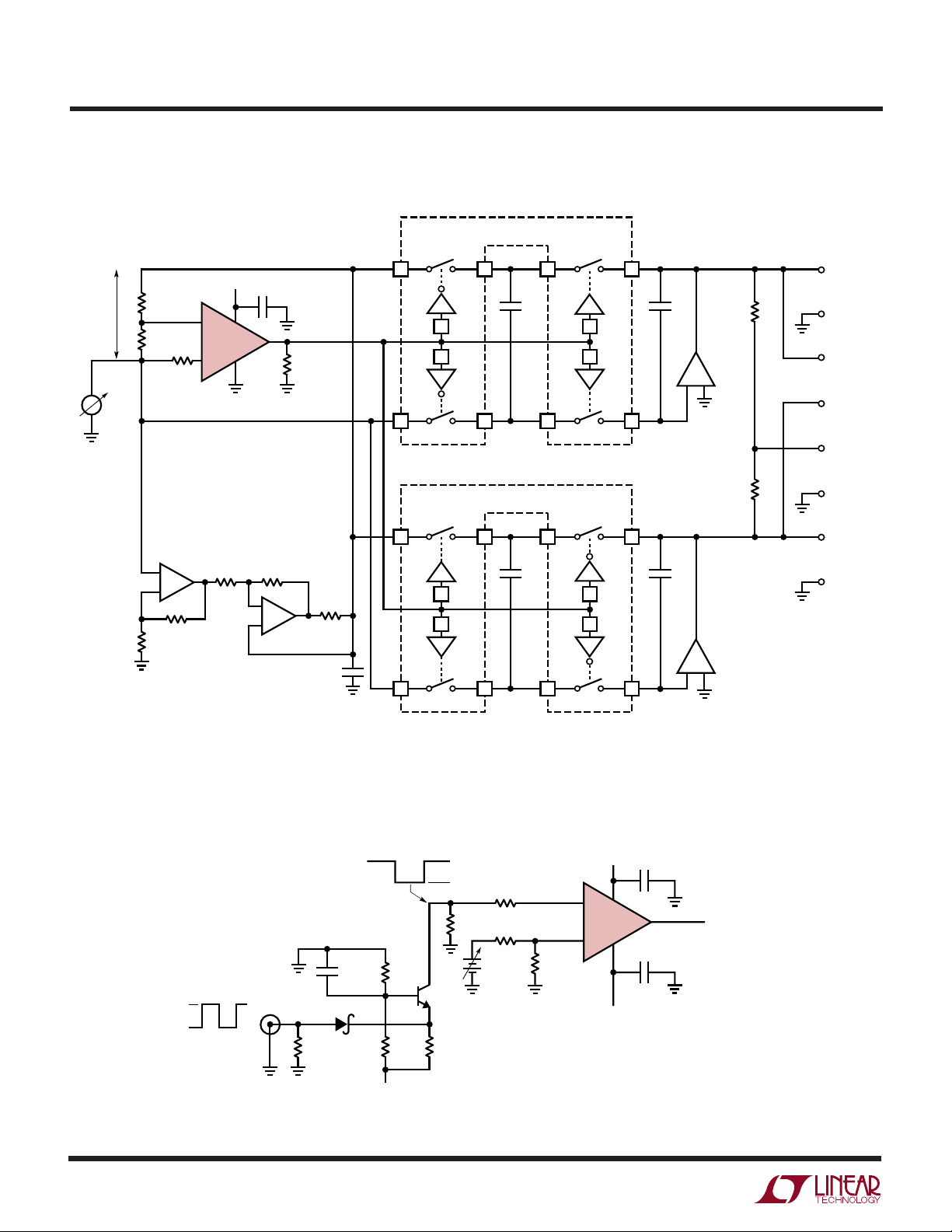
TEST CIRCUITS
15V
P-P
BANDWIDTH-LIMITED
TRIANGLE WAVE
~
1kHz
V
CC
50k
50Ω
50Ω
DUT
V
1/2 LT1720 OR
CM
NOTES: LT1638, LT1112, LTC203s ARE POWERED FROM ±15V.
1/4 LT1721
1/2 LT1638
+
–
100k
100k
200kΩ PULL-DOWN PROTECTS LTC203 LOGIC INPUTS
WHEN DUT IS NOT POWERED
0.1µF
+
–
100k
100k
+
–
1/2 LT1638
200k
2.4k
0.15µF
±V
LTC203
LTC203
Test Circuit
TRIP
16
9
1
8
15 3 214
1000 × V
TRIP
HYST
OS
TRIP
+
–
1000 × V
10k
1000 × V
10k
1000 × V
1720/21 TC01
1µF
1µF
–
–
1/2 LT1112
+
1/2 LT1112
+
10nF
1
8
10 6 711
2 14 153
10nF
16
9
7 11 106
6
–3V
Response Time Test Circuit
– V
+V
CC
+
–
TRIP
–V
CM
0.01µF
10 × SCOPE PROBE
(C
≈ 10pF)
IN
0.01µF
CM
+
)
1720/21 TC02
0V
–100mV
25Ω
0.1µF
0V
PULSE
IN
1N5711
50Ω
–5V
130Ω
400Ω
2N3866
750Ω
V1*
*V1 = –1000 • (OVERDRIVE + V
NOTE: RISING EDGE TEST SHOWN.
FOR FALLING EDGE, REVERSE LT1720 INPUTS
1/2 LT1720 OR
25Ω
50k
50Ω
DUT
1/4 LT1721

LT1720/LT1721
U
WUU
APPLICATIONS INFORMATION
Input Voltage Considerations
The LT1720/LT1721 are specified for a common mode
range of –100mV to 3.8V when used with a single 5V
supply. In general the common mode range is 100mV
below ground to 1.2V below VCC. The criterion for this
common mode limit is that the output still responds
correctly to a small differential input signal. Also, if one
input is within the common mode limit, the other input
signal can go outside the common mode limits, up to the
absolute maximum limits (a diode drop past either rail at
10mA input current) and the output will retain the correct
polarity.
When either input signal falls below the negative common
mode limit, the internal PN diode formed with the substrate can turn on, resulting in significant current flow
through the die. An external Schottky clamp diode
between the input and the negative rail can speed up
recovery from negative overdrive by preventing the substrate diode from turning on.
When both input signals are below the negative common
mode limit, phase reversal protection circuitry prevents
false output inversion to at least –400mV common mode.
However, the offset and hysteresis in this mode will
increase dramatically, to as much as 15mV each. The input
bias currents will also increase.
When both input signals are above the positive common
mode limit, the input stage will become debiased and the
output polarity will be random. However, the internal
hysteresis will hold the output to a valid logic level, and
because the biasing of each comparator is completely
independent, there will be no impact on any other comparator. When at least one of the inputs returns to within
the common mode limits, recovery from this state will take
as long as 1µs.
The propagation delay does not increase significantly
when driven with large differential voltages. However, with
low levels of overdrive, an apparent increase may be seen
with large source resistances due to an RC delay caused
by the 2pF typical input capacitance.
Input Protection
The input stage is protected against damage from large
differential signals, up to and beyond a differential voltage
equal to the supply voltage, limited only by the absolute
maximum currents noted. External input protection circuitry is only needed if currents would otherwise exceed
these absolute maximums. The internal catch diodes can
conduct current up to these rated maximums without
latchup, even when the supply voltage is at the absolute
maximum rating.
The LT1720/LT1721 input stage has general purpose
internal ESD protection for the human body model. For use
as a line receiver, additional external protection may be
required. As with most integrated circuits, the level of
immunity to ESD is much greater when residing on a
printed circuit board where the power supply decoupling
capacitance will limit the voltage rise caused by an ESD
pulse.
Input Bias Current
Input bias current is measured with both inputs held at 1V.
As with any PNP differential input stage, the LT1720/
LT1721 bias current flows out of the device. With a
differential input voltage of even just 100mV or so, there
will be zero bias current into the higher of the two inputs,
while the current flowing out of the lower input will be
twice the measured bias current. With more than two
diode drops of differential input voltage, the LT1720/
LT1721’s input protection circuitry activates, and current
out of the lower input will increase an additional 30% and
there will be a small bias current into the higher of the two
input pins, of 4µA or less. See the Typical Performance
curve “Input Current vs Differential Input Voltage.”
High Speed Design Considerations
Application of high speed comparators is often plagued
by oscillations. The LT1720/LT1721 have 4mV of internal
hysteresis, which will prevent oscillations as long as
parasitic output to input feedback is kept below 4mV.
7
LT1720/LT1721
U
WUU
APPLICATIONS INFORMATION
However, with the 2V/ns slew rate of the LT1720/LT1721
outputs, a 4mV step can be created at a 100Ω input
source with only 0.02pF of output to input coupling. The
pinouts of the LT1720/LT1721 have been arranged to
minimize problems by placing the most sensitive inputs
(inverting) away from the outputs, shielded by the power
rails. The input and output traces of the circuit board
should also be separated, and the requisite level of
isolation is readily achieved if a topside ground plane runs
between the outputs and the inputs. For multilayer boards
where the ground plane is internal, a topside ground or
supply trace should be run between the inputs and
outputs, as illustrated in Figure 1.
(b)(a)
1720/21 F01
Figure 1. Typical Topside Metal for Multilayer PCB Layouts
Figure 1a shows a typical topside layout of the LT1720 on
such a multilayer board. Shown is the topside metal etch
including traces, pin escape vias, and the land pads for an
SO-8 LT1720 and its adjacent X7R 10nF bypass capacitor
in a 1206 case.
The ground trace from Pin 5 runs under the device up to
the bypass capacitor, shielding the inputs from the
outputs. Note the use of a common via for the LT1720 and
the bypass capacitor, which minimizes interference from
high frequency energy running around the ground plane or
power distribution traces.
The supply bypass should include an adjacent
10nF ceramic capacitor and a 2.2µF tantalum capacitor no
farther than 5cm away; use more capacitance if driving
more than 4mA loads. To prevent oscillations, it is helpful
to balance the impedance at the inverting and noninverting
inputs; source impedances should be kept low, preferably
1kΩ or less.
The outputs of the LT1720/LT1721 are capable of very
high slew rates. To prevent overshoot, ringing and other
problems with transmission line effects, keep the output
traces shorter than 10cm, or be sure to terminate the lines
to maintain signal integrity. The LT1720/LT1721 can drive
DC terminations of 250Ω or more, but lower characteristic
impedance traces can be driven with series termination or
AC termination topologies.
Hysteresis
The LT1720/LT1721 include internal hysteresis, which
makes them easier to use than many other comparable
speed comparators.
The input-output transfer characteristic is illustrated in
Figure 2 showing the definitions of VOS and V
HYST
based
upon the two measurable trip points. The hysteresis band
makes the LT1720/LT1721 well behaved, even with slowly
moving inputs.
OUT
V
V
HYST
+
–
– V
(= V
TRIP
TRIP
V
HYST
)
/2
V
OH
Figure 1b shows a typical topside layout of the LT1721 on
a multilayer board. In this case, the power and ground
traces have been extended to the bottom of the device
solely to act as high frequency shields between input and
output traces.
Although both VCC pins are electrically shorted internal to
the LT1721, they must be shorted together externally as
well in order for both to function as shields. The same is
true for the two GND pins.
8
V
OL
0
–
V
TRIP
V
Figure 2. Hysteresis I/O Characteristics
+
V
+ V
TRIP
=
OS
TRIP
2
V
TRIP
–
+
∆VIN = V
1720/21 F02
+
–
– V
IN
IN

LT1720/LT1721
U
WUU
APPLICATIONS INFORMATION
The exact amount of hysteresis will vary from part to part
as indicated in the specifications table. The hysteresis level
will also vary slightly with changes in supply voltage and
common mode voltage. A key advantage of the LT1720/
LT1721 is the significant reduction in these effects, which
is important whenever an LT1720/LT1721 is used to detect a threshold crossing in one direction only. In such a
case, the relevant trip point will be all that matters, and a
stable offset voltage with an unpredictable level of hysteresis, as seen in competing comparators, is of little value.
The LT1720/LT1721 are many times better than prior comparators in these regards. In fact, the CMRR and PSRR
tests are performed by checking for changes in either trip
point to the limits indicated in the specifications table.
Because the offset voltage is the average of the trip points,
the CMRR and PSRR of the offset voltage is therefore
guaranteed to be at least as good as those limits. This
more stringent test also puts a limit on the common mode
and power supply dependence of the hysteresis voltage.
Additional hysteresis may be added externally. The rail-torail outputs of the LT1720/LT1721 make this more predictable than with TTL output comparators due to the
LT1720/LT1721’s small variability of VOH (output high
voltage).
To add additional hysteresis, set up positive feedback by
adding additional external resistor R3 as shown in Figure
3. Resistor R3 adds a portion of the output to the threshold
set by the resistor string. The LT1720/LT1721 pulls the
outputs to the supply rail and ground to within 200mV of
the rails with light loads, and to within 400mV with heavy
loads. For the load of most circuits, a good model for the
voltage on the right side of R3 is 300mV or VCC – 300mV,
for a total voltage swing of (VCC – 300mV) – 300mV =
VCC – 600mV.
With this in mind, calculation of the resistor values needed
is a two-step process. First, calculate the value of R3 based
on the additional hysteresis desired, the output voltage
swing, and the impedance of the primary bias string:
R3 = (R1R2)(VCC – 0.6V)/(additional hysteresis)
Additional hysteresis is the desired overall hysteresis less
the internal 3.5mV hysteresis.
The second step is to recalculate R2 to set the same
average threshold as before. The average threshold before
was set at VTH = (V
)(R1)/(R1 + R2). The new R2 is
REF
calculated based on the average output voltage (VCC/2)
and the simplified circuit model in Figure 4. To assure that
the comparator’s noninverting input is, on average, the
same VTH as before:
R2′ = (V
– VTH)/(VTH/R1 + (VTH – VCC/2)/R3)
REF
For additional hysteresis of 10mV or less, it is not uncommon for R2′ to be the same as R2 within 1% resistor
tolerances.
This method will work for additional hysteresis of up to a
few hundred millivolts. Beyond that, the impedance of R3
is low enough to effect the bias string, and adjustment of
R1 may also be required. Note that the currents through
the R1/R2 bias string should be many times the input
currents of the LT1720/LT1721. For 5% accuracy, the
current must be at least 120µA(6µA IB ÷ 0.05); more for
higher accuracy.
V
REF
R2
R1
INPUT
Figure 3. Additional External Hysteresis
R3
+
1/2 LT1720
–
1720/21 F03
V
REF
R2′
V
TH
R1
Figure 4. Model for Additional Hysteresis Calculations
R3
+
1/2 LT1720
–
V
AVERAGE
V
=
1720/21 F04
CC
2
9
 Loading...