

FEATURES
LT1716
SOT-23, 44V, Over-The-Top,
Micropower, Precision
Rail-to-Rail Comparator
U
DESCRIPTIO
■
Operates from 2.7V to 44V
■
Over-The-Top®: Input Common Mode Range
Extends 44V Above V–, Independent of V
■
Micropower: 35µA I
■
Offset Voltage: 1.5mV Max
■
5-Pin SOT-23 Package
■
Valid Output with Either Input 5V Below V
■
Rail-to-Rail Output Swing
■
Output Can Drive Loads Above V
■
Internal Pull-Up Current
■
–40°C to 125°C Operating Temperature Range
Q
+
U
APPLICATIO S
■
Power Supply Monitors
■
Relay/Lamp Driver
■
Oscillators
■
Peak Detector
■
Level Shifting
The LT®1716 comparator operates on any total power
supply voltage between 2.7V and 44V drawing 35µA of
+
quiescent current. The LT1716 has a unique input stage
that can be taken 44V above V–, independent of V+ supply.
(Built-in resistors protect the inputs for faults below the
negative supply of up to 5V.) The inputs can withstand 44V
–
both differential and common mode.
The output stage includes a class “B” pull-up current
source, eliminating the need for an external resistive pullup and saving power. Output voltage swings to within
35mV of the negative supply and 55mV of the positive
supply, which makes the comparator a good choice for
low voltage single supply operation. The output stage is
also designed to drive loads connected to a higher supply
than the LT1716 supply, the same as an open collector
output stage.
The LT1716 is available in a SOT-23 5-lead package.
, LTC and LT are registered trademarks of Linear Technology Corporation.
Over-The-Top is a registered trademark of Linear Technology Corporation.
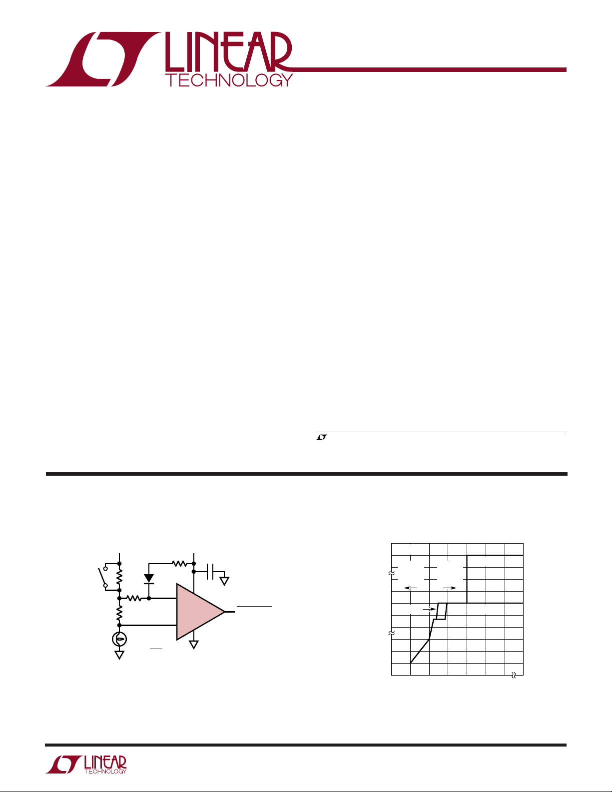
TYPICAL APPLICATIO
Lamp Monitor
LAMP
ON/OFF
0.15Ω
0.25A TO 2.5A
5V TO 44V
100k
R
S
1W
5k
RS ≥
CMPD6001
0.04
I
L
1M
4
–
LT1716 LAMP GOOD
3
+
U
Input Bias Current vs Input Bias Voltage
(A)
–
B
I
–100µ
–0.5m
–1.5m
12µ
VS = 5V, 0V
8µ
INPUT
4µ
BELOW
6n
SUPPLY
3n
0
+IN = 2V +IN = 2V
–3n
–6n
–1m
–5 0 5 10 15 20 45
–10
INPUT
ABOVE
SUPPLY
+IN = 10V
–
V
(V)
IN
1716 TA02
1716f
3V
0.1µF
5
1
2
1716 TA01
1
LT1716
WW
W
ABSOLUTE AXI U RATI GS
U
UUW
PACKAGE/ORDER I FOR ATIO
(Note 1)
Supply Voltage (V+ to V–)........................................ 44V
Differential Input Voltage ......................................... 44V
Input Voltage ...................................................44V, –5V
Output Short-Circuit Duration (Note 2)............ Indefinite
Operating Temperature Range (Note 3)
LT1716C/LT1716I ............................. – 40°C to 85°C
LT1716H .......................................... –40°C to 125°C
Specified Temperature Range (Note 4)
TOP VIEW
OUT
1
–
V
2
+IN
T
JMAX
+
3
S5 PACKAGE
5-LEAD PLASTIC SOT-23
= 150°C, θJA = 250°C/W
+
54V
–
–IN
ORDER PART NUMBER
LT1716CS5
LT1716IS5
LT1716HS5
S5 PART MARKING*
LTYD
LT1716C/LT1716I ............................. – 40°C to 85°C
LT1716H .......................................... –40°C to 125°C
Maximum Junction Temperature .......................... 150°C
Storage Temperature Range ................. –65°C to 150°C
*The temperature grades are identified by a label on the shipping container.
Consult LTC Marketing for parts specified with wider operating temperature ranges.
Lead Temperature (Soldering, 10 sec)..................300°C
ELECTRICAL CHARACTERISTICS
temperature range of –40°C ≤ TA ≤ 85°C, otherwise specifications are at TA = 25°C. Single supply operation V+ = 5V, V– = 0V;
VCM = V+/2 unless otherwise noted. (Note 4)
The ● denotes the specifications which apply over the full operating
LT1716C/LT1716I
SYMBOL PARAMETER CONDITIONS MIN TYP MAX UNITS
V
OS
I
OS
I
B
CMRR Common Mode Rejection Ratio 0.5V ≤ VCM < (V+ – 1V) ● 89 110 dB
PSRR Power Supply Rejection Ratio V– = 0V, VCM = 1.5V; 2.7V < V+ < 36V ● 95 110 dB
A
VOL
I
S
Input Offset Voltage 0.5V < VCM < (VCC – 1V) 300 1600 µV
0°C < TA < 70°C ● 2100 µV
–40°C < T
Input Offset Voltage Drift 0°C < TA < 70°C ● 2 µV/°C
(Note 5) –40°C < TA < 85°C ● 2 µV/°C
Input Offset Current VCM = V+/2 ● 315 nA
VCM = 0V ● 1.3 µA
V
CM
Input Bias Current VCM = V+/2 20 50 nA
V+ = 0V, VCM = 44V 2 nA
V
CM
V
CM
VCM = –5V ● 1 1.4 mA
Input Voltage Range (Note 7) ● 0.5 44 V
0.5V ≤ V
Minimum Operating Supply Voltage ● 2.4 2.7 V
Large-Signal Voltage Gain RL = 1k; 1V < V
Supply Current V+ = 3V, RL = Open, VO = High 35 50 µA
V+ = 5V, RL = Open, VO = High 35 55 µA
V+ = 12V, RL = Open, VO = High 40 60 µA
< 85°C ● 2500 µV
A
= 44V ● 0.9 µA
● 35 75 nA
= 0V ● 313 µA
= 44V ● 69 µA
< 44V, (Note 6) ● 81 110 dB
CM
< 4V 200 500 V/mV
OUT
● 100 V/mV
● 65 µA
● 75 µA
● 85 µA
2
1716f
LT1716
ELECTRICAL CHARACTERISTICS
The ● denotes the specifications which apply over the full operating
temperature range of –40°C ≤ TA ≤ 85°C, otherwise specifications are at TA = 25°C. Single supply operation V+ = 5V, V– = 0V;
VCM = V+/2 unless otherwise noted. (Note 4)
SYMBOL PARAMETER CONDITIONS MIN TYP MAX UNITS
–
I
SC
+
I
SC
V
OL
V
OH
Output Sink Current (Note 2) V
Output Source Current V
Output Voltage Swing Low I
(Referred to V
Output Voltage Swing High I
(Referred to V
–
)I
+
)I
Leakage Current V
Propagation Delay V
OVERDRIVE
OVERDRIVE
SINK
SINK
I
SINK
I
SINK
SOURCE
SOURCE
OUT
OVERDRIVE
> 30mV ● 10 20 mA
= 5mV, V
= 0mA, V
OVERDRIVE
= 1V ● 60 85 µA
OUT
= –10mV ● 20 35 mV
= 0.1mA ● 75 110 mV
= 1mA ● 200 300 mV
= 5mA ● 550 900 mV
= 0µA, V
OVERDRIVE
= 10mV ● 30 55 mV
= 10µA ● 130 185 mV
= 40V, V
> 100mV, R
OVERDRIVE
> 100mV ● 0.5 2 µA
= 10k 3 5.5 µs
LOAD
LT1716C/LT1716I
The ● denotes the specifications which apply over the full operating temperature range of –40°C ≤ TA ≤ 85°C, otherwise specifications
are at TA = 25°C. Split supply operation VS = ±15V, VCM = 0V unless otherwise noted. (Note 4)
LT1716C/LT1716I
SYMBOL PARAMETER CONDITIONS MIN TYP MAX UNITS
V
OS
I
OS
I
B
CMRR Common Mode Rejection Ratio –14.5V < VCM < 14V ● 92 110 dB
PSRR Power Supply Rejection Ratio VS = ±1.35V to ±22V ● 90 110 dB
A
VOL
I
S
–
I
SC
+
I
SC
V
OL
Input Offset Voltage –14.5V < VCM < 14V 300 1500 µV
0°C < T
< 70°C ● 2000 µV
A
–40°C < T
< 85°C ● 2400 µV
A
Input Offset Voltage Drift (Note 5) 0°C < TA < 70°C ● 2 µV/°C
–40°C < T
< 85°C ● 2 µV/°C
A
Input Offset Current VCM = 0V ● 315 nA
= 29V ● 0.9 µA
V
CM
V
= –15V ● 1.3 µA
CM
Input Bias Current VCM = 0V 30 60 nA
● 50 100 nA
VCM = 29V ● 69 µA
= –15V ● 313 µA
V
CM
V
= –20V ● 1 1.4 mA
CM
Input Voltage Range (Note 7) ● –14.5 14 V
–14.5V < V
< 29V (Note 6) ● 81 98 dB
CM
Minimum Operating Supply Voltage ● 2.4 2.7 V
Large-Signal Voltage Gain RL = 6k; –14V < V
< 14V 500 1000 V/mV
OUT
● 400 V/mV
Supply Current VS = ±15V, RL = Open, VO = High ● 40 95 µA
Output Sink Current (Note 2) V
Output Source Current V
Output Voltage Swing Low I
(Referred to V
–
)I
OVERDRIVE
OVERDRIVE
SINK
SINK
I
SINK
I
SINK
> 30mV ● 10 20 mA
= 5mV, V
= 0mA, V
OVERDRIVE
= –14V ● 70 105 µA
OUT
= –10mV ● 20 35 mV
= 0.1mA ● 75 110 mV
= 1mA ● 200 300 mV
= 5mA ● 550 900 mV
1716f
3

LT1716
ELECTRICAL CHARACTERISTICS
The ● denotes the specifications which apply over the full operating
temperature range of –40°C ≤ TA ≤ 85°C, otherwise specifications are at TA = 25°C. Split supply operation VS = ±15V, VCM = 0V
unless otherwise noted. (Note 4)
LT1716C/LT1716I
SYMBOL PARAMETER CONDITIONS MIN TYP MAX UNITS
V
OH
Output Voltage Swing High I
(Referred to V
+
)I
Leakage Current V
Propagation Delay V
= 0µA, V
SOURCE
= 10µA ● 140 210 mV
SOURCE
= 25V, V
OUT
OVERDRIVE
OVERDRIVE
OVERDRIVE
> 100mV, R
= 10mV ● 45 75 mV
> 100mV ● 0.6 2 µA
= 10k 5.5 9 µs
LOAD
The ● denotes the specifications which apply over the operating temperature range of –40°C < TA < 125°C, otherwise specifications
are at TA = 25°C. Single supply operation V+ = 5V, V– = 0V, VCM = VCC/2 unless otherwise noted. (Note 4)
LT1716H
SYMBOL PARAMETER CONDITIONS MIN TYP MAX UNITS
V
OS
I
OS
I
B
CMRR Common Mode Rejection Ratio 0.5V < VCM < (V+ – 1V) ● 75 110 dB
PSRR Power Supply Rejection Ratio V– = 0V, VCM = 1.5V, 2.7V < V+ < 36V ● 85 110 dB
A
VOL
I
S
–
I
SC
+
I
SC
V
OL
V
OH
Input Offset Voltage 0.5V < VCM < (VCC – 1V) 300 1600 µV
● 2900 µV
Input Offset Voltage Drift (Note 5) ● 2 µV/°C
Input Offset Current VCM = V+/2 ● 3 220 nA
V
= 0V ● 1.3 µA
CM
= 44V ● 0.9 µA
V
CM
Input Bias Current VCM = V+/2 20 50 nA
● 900 nA
V+ = 0V, VCM = 44V 2 nA
= 0V ● 325 µA
V
CM
V
= 44V ● 614 µA
CM
= –5V ● 1 1.4 mA
V
CM
Input Voltage Range (Note 7) 0.5 44 V
0.5V < V
< 44V (Note 6) ● 72 110 dB
CM
Minimum Operating Supply Voltage ● 2.4 2.7 V
Large-Signal Voltage Gain RL = 1k, 1V < V
= 6k ● 20 V/mV
R
L
< 4V 200 500 V/mV
OUT
Supply Current per Amplifier V+ = 3V, RL = Open, VO = High 35 50 µA
● 70 µA
V+ = 5V, RL = Open, VO = High 35 55 µA
● 75 µA
V+ = 12V, RL = Open, VO = High 40 60 µA
● 85 µA
Output Sink Current (Note 2) V
Output Source Current V
Output Voltage Swing Low I
(Referred to V
–
)I
Output Voltage Swing High I
(Referred to V+) I
Leakage Current V
Propagation Delay V
OVERDRIVE
OVERDRIVE
SINK
SINK
I
SINK
I
SINK
SOURCE
SOURCE
OUT
OVERDRIVE
> 30mV ● 510 mA
= 5mV, V
= 0mA, V
OVERDRIVE
= 1V ● 60 110 µA
OUT
= –10mV ● 20 60 mV
= 0.1mA ● 75 170 mV
= 1mA ● 200 480 mV
= 5mA ● 550 1200 mV
= 0µA, V
OVERDRIVE
= –10mV ● 50 110 mV
= 10µA ● 130 220 mV
= 40V, V
> 100mV, R
OVERDRIVE
> 100mV ● 1.7 5 µA
= 10k 6 9 µs
LOAD
1716f
4
 Loading...