


LT1715
4ns, 150MHz
Dual Comparator with
Independent Input/Output Supplies
FEATURES
n
UltraFast: 4ns at 20mV Overdriven
n
150MHz Toggle Frequency
n
Separate Input and Output Power Supplies
n
Low Power: 4.6mA per Comparator at 3V
n
Pinout Optimized for High Speed Use
n
Output Optimized for 3V and 5V Supplies
n
TTL/CMOS Compatible Rail-to-Rail Output
n
Input Voltage Range Extends 100mV
Below Negative Rail
n
Internal Hysteresis with Specifi ed Limits
n
Specifi ed for –40°C to 125°C Temperature Range
n
Available in the 10-pin MSOP Package
APPLICATIONS
n
High Speed Differential Line Receivers
n
Level Translators
n
Window Comparators
n
Crystal Oscillator Circuits
n
Threshold Detectors/Discriminators
n
High Speed Sampling Circuits
n
Delay Lines
DESCRIPTION
The LT®1715 is an UltraFast™ dual comparator optimized for
low voltage operation. Separate supplies allow independent
analog input ranges and output logic levels with no loss of
performance. The input voltage range extends from 100mV
below V
LT1715 easy to use even with slow moving input signals.
The rail-to-rail outputs directly interface toTTL and CMOS.
The symmetric output drive results in similar rise and fall
times that can be harnessed for analog applications or for
easy translation to other single supply logic levels.
The LT1715 is available in the 10-pin MSOP package. The
pinout of the LT1715 minimizes parasitic effects by placing
the most sensitive inputs away from the outputs, shielded
by the power rails.
For a dual/quad single supply comparator with similar propagation delay, see the LT1720/LT1721. For a
single comparator with similar propagation delay, see
the LT1719.
L, LT, LTC and LTM are registered trademarks of Linear Technology Corporation.
UltraFast is a trademark of Linear Technology Corporation.
to 1.2V below VCC. Internal hysteresis makes the
EE
TYPICAL APPLICATION
100MHz Dual Differential Line Receiver
5V 3V
+
IN A
–
+
IN B
–
–5V
1715 TA01
OUT A
OUT B
CLOCK OUT
DATA OUT
Line Receiver Response to 100MHz Clock,
50MHz Data Both with 25mV
3V
0V
3V
0V
FET PROBES
5ns/DIV
P-P
Inputs
1715 TA02
1V/DIV
1V/DIV
1715fa
1

LT1715
(Note 1)
Supply Voltage
to GND .............................................................7V
+V
S
to VEE ..........................................................13.2V
V
CC
to VEE ..........................................................13.2V
+V
S
to GND ......................................... –13.2V to 0.3V
V
EE
Input Current (+IN, –IN) .......................................±10mA
Output Current (Continuous) ...............................±20mA
Operating Temperature Range (Note 2)
LT1715C ............................................... –40°C to 85°C
LT1715I ................................................ –40°C to 85°C
LT1715H ............................................–40°C to 125°C
Specifi ed Temperature Range (Note 3)
LT1715C ................................................... 0°C to 70°C
LT1715I ................................................ –40°C to 85°C
LT1715H ............................................ –40°C to 125°C
Junction Temperature ........................................... 150°C
Storage Temperature Range ................... –65°C to 150°C
Lead Temperature (Soldering, 10 sec) ..................300°C
PIN CONFIGURATION ABSOLUTE MAXIMUM RATINGS
TOP VIEW
10
1
+IN A
–IN A
–IN B
+IN B
V
EE
10-LEAD PLASTIC MSOP
T
= 150°C, θJA = 120°C/W (NOTE 4)
JMAX
2
3
4
5
MS PACKAGE
A
B
V
CC
+V
9
S
OUT A
8
OUT B
7
GND
6
ORDER INFORMATION
LEAD FREE FINISH TAPE AND REEL PART MARKING PACKAGE DESCRIPTION SPECIFIED TEMPERATURE RANGE
LT1715CMS#PBF LT1715CMS#TRPBF LTVQ 10-Lead Plastic MSOP 0°C to 70°C
LT1715IMS#PBF LT1715IMS#TRPBF LTVV 10-Lead Plastic MSOP –40°C to 85°C
LT1715HMS#PBF LT1715HMS#TRPBF LTVV 10-Lead Plastic MSOP –40°C to 125°C
Consult LTC Marketing for parts specifi ed with wider operating temperature ranges.
Consult LTC Marketing for information on non-standard lead based fi nish parts.
For more information on lead free part marking, go to:
For more information on tape and reel specifi cations, go to:
The l denotes the specifi cations which apply over the full operating
ELECTRICAL CHARACTERISTICS
temperature range, otherwise specifi cations are at T
unless otherwise specifi ed.
SYMBOL PARAMETER CONDITIONS MIN TYP MAX UNITS
V
+V
V
V
V
CC
S
CMR
TRIP
TRIP
– V
+
–
EE
Input Supply Voltage
Output Supply Voltage
Input Voltage Range (Note 5)
Input Trip Points (Note 6) LT1715C, LT1715I
Input Trip Points (Note 6) LT1715C, LT1715I
http://www.linear.com/leadfree/
http://www.linear.com/tapeandreel/
= 25°C. VCC = 5V, VEE = –5V, +VS = 5V, VCM = 1V, C
A
LT1715H
LT1715H
= 10pF, V
OUT
l
2.7 12 V
l
2.7 6 V
l
VEE – 0.1 VCC – 1.2 V
l
–1.5
l
–1.8
l
–5.5
l
–6
OVERDRIVE
5.5
6
1.5
1.8
= 20mV,
mV
mV
mV
mV
2
1715fa
LT1715
ELECTRICAL CHARACTERISTICS
The l denotes the specifi cations which apply over the full operating
temperature range, otherwise specifi cations are at T
= 25°C. VCC = 5V, VEE = –5V, +VS = 5V, VCM = 1V, C
A
unless otherwise specifi ed.
SYMBOL PARAMETER CONDITIONS MIN TYP MAX UNITS
V
OS
V
HYST
VOS/ΔT Input Offset Voltage Drift
I
B
I
OS
CMRR Common Mode Rejection Ratio (Note 7) LT1715C, LT1715I
PSRR Power Supply Rejection Ratio (Note 8)
A
V
V
OH
V
OL
f
MAX
t
PD20
t
PD5
t
SKEW
Δt
PD
t
r
t
f
t
JITTER
I
CC
I
EE
I
S
Input Offset Voltage (Note 6)
LT1715C, LT1715I
LT1715H
Input Hysteresis Voltage (Note 6) LT1715C, LT1715I
LT1715H
Input Bias Current LT1715C, LT1715I
LT1715H
Input Offset Current LT1715C, LT1715I
LT1715H
LT1715H
l
l
l
l
l
l
l
l
l
l
l
l
Voltage Gain (Note 9) ∞
Output High Voltage I
Output Low Voltage I
= 4mA, VIN = V
SOURCE
= 10mA, VIN = V
SINK
TRIP
TRIP
+
+ 20mV
–
– 20mV
l
+VS – 0.4 V
l
Maximum Toggle Frequency (Note 10) 150 MHz
Propagation Delay V
OVERDRIVE
V
CC
LT1715H
V
OVERDRIVE
V
OVERDRIVE
LT1715C, LT1715I
LT1715H
Propagation Delay V
OVERDRIVE
Propagation Delay Skew (Note 13) Between t
Differential Propagation Delay (Note 14) Between Channels
= 20mV (Note 11),
= 5V, VEE = –5V LT1715C, LT1715I
l
l
= 20mV, VCC = 5V, VEE = 0V 4.4 ns
= 20mV, VCC = 3V, VEE = 0V
l
l
= 5mV, VEE = 0V (Notes 11, 12)
l
+
PD
/t
PD
–
, VEE = 0V
l
l
Output Rise Time 10% to 90% 2 ns
Output Fall Time 90% to 10% 2 ns
Output Timing Jitter VIN = 1.2V
f = 20MHz (Note 15) t
Positive Input Stage Supply Current
(per Comparator)
+VS = VCC = 5V, VEE = –5V LT1715C, LT1715I
LT1715H
+VS = VCC = 3V, VEE = 0V LT1715C, LT1715I
LT1715H
Negative Input Stage Supply Current
(per Comparator)
+VS = VCC = 5V, VEE = –5V LT1715C, LT1715I
LT1715H
+VS = VCC = 3V, VEE = 0V LT1715C, LT1715I
LT1715H
Positive Output Stage Supply Current
(per Comparator)
+VS = VCC = 5V, VEE = –5V LT1715C, LT1715I
LT1715H
VS = VCC = 3V, VEE = 0V LT1715C, LT1715I
LT1715H
(6dBm), ZIN = 50 t
P-P
PD
PD
+
–
l
l
l
l
l
l
l
l
l
l
l
l
= 10pF, V
OUT
OVERDRIVE
= 20mV,
0.4 2.5
3.5
4
2
2
3.5 6
7
10 μV/°C
–6
–7
–2.5 0
0
0.2 0.6
1
60
70 dB
55
65 80 dB
0.4 V
2.8
2.8
2.8
3
3
3
46
7
8
4.8 6.5
7.5
8
6912ns
0.5 1.5 ns
0.3 1 ns
15
11
ps
ps
12
2.2
0.9 1.6
1.8
–4.8
–2.9 mA
–5.3
–3.8
–2.4 mA
–4.3
4.6 7.5
8
3.7 6
6.5
mV
mV
mV
mV
mV
μA
μA
μA
μA
dB
RMS
RMS
mA
mA
mA
mA
mA
mA
mA
mA
mA
mA
ns
ns
ns
ns
ns
ns
ns
1715fa
3
LT1715
ELECTRICAL CHARACTERISTICS
Note 1: Stresses beyond those listed under Absolute Maximum Ratings
may cause permanent damage to the device. Exposure to any Absolute
Maximum Rating condition for extended periods may affect device
reliability and lifetime.
Note 2: The LT1715C is guaranteed functional over the operating range of
–40°C to 85°C.
Note 3: The LT1715C is guaranteed to meet specifi ed performance from
0°C to 70°C. The LT1715°C is designed, characterized and expected to
meet specifi ed performance from –40°C to 85°C but is not tested or
QA sampled at these temperatures. The LT1715I is guaranteed to meet
specifi ed performance from –40°C to 85°C. The LT1715H is guaranteed to
meet specifi ed performance from –40°C to 125°C.
Note 4: Thermal resistances vary depending upon the amount of PC board
metal attached to Pin 5 of the device. θ
FR-4 board covered with 2oz copper on both sides and with 100mm
is specifi ed for a 2500mm2 3/32"
JA
2
of
copper attached to Pin 5. Thermal performance can be improved beyond
the given specifi cation by using a 4-layer board or by attaching more metal
area to Pin 5.
Note 5: If one input is within these common mode limits, the other input
can go outside the common mode limits and the output will be valid.
Note 6: The LT1715 comparator includes internal hysteresis. The trip
points are the input voltage needed to change the output state in each
direction. The offset voltage is defi ned as the average of V
TRIP
+
and V
TRIP
–
,
while the hysteresis voltage is the difference of these two.
Note 7: The common mode rejection ratio is measured with V
V
= –5V and is defi ned as the change in offset voltage measured from
EE
V
= –5.1V to VCM = 3.8V, divided by 8.9V.
CM
CC
= 5V,
Note 8: The power supply rejection ratio is measured with VCM = 1V and is
defi ned as the worst of: the change in offset voltage from V
to V
= +VS = 6V (with VEE = 0V) divided by 3.3V or the change in offset
CC
voltage from V
= 0V to VEE = –6V (with VCC = +VS = 6V) divided by 6V.
EE
= +VS = 2.7V
CC
Note 9: Because of internal hysteresis, there is no small-signal region in
which to measure gain. Proper operation of internal circuity is ensured by
measuring V
and VOL with only 20mV of overdrive.
OH
Note 10: Maximum toggle rate is defi ned as the highest frequency at
which a 100mV sinusoidal input results in an error free output toggling to
greater than 4V when high and to less than 1V when low on a 5V output
supply.
Note 11: Propagation delay measurements made with 100mV steps.
Overdrive is measured relative to V
Note 12: t
cannot be measured in automatic handling equipment with
PD
TRIP
±
.
low values of overdrive. The LT1715 is 100% tested with a 100mV step
and 20mV overdrive. Correlation tests have shown that t
limits can be
PD
guaranteed with this test.
Note 13: Propagation Delay Skew is defi ned as:
t
SKEW
= |t
PDLH
– t
PDHL
|
Note 14: Differential propagation delay is defi ned as the larger of the two:
Δt
Δt
PDLH
PDHL
= |t
= |t
PDLHA
PDHLA
– t
– t
PDLHB
PDHLB
|
|
Note 15: Package inductances combined with asynchronous activity on
the other channel can increase the output jitter. See Channel Interactions
in Applications Information. Specifi cation above is with one channel active
only.
TYPICAL PERFORMANCE CHARACTERISTICS
Input Offset and Trip Voltages
vs Supply Voltage
3
2
1
0
–1
AND TRIP POINT VOLTAGE (mV)
TA = 25°C
–2
OS
V
= 1V
V
CM
= GND
V
EE
–3
2.5
3.0 3.5
SUPPLY VOLTAGE, VCC = +VS (V)
V
V
4.0 5.0
+
TRIP
V
OS
–
TRIP
4.5 5.5 6.0
1715 G01
Input Offset and Trip Voltages
vs Temperature
3
+VS = VCC = 5V
= 1V
V
CM
2
= –5V
V
EE
1
0
–1
AND TRIP POINT VOLTAGE (mV)
–2
OS
V
–3
–20 20 60 100
TEMPERATURE (°C)
+
V
TRIP
V
OS
–
V
TRIP
4
1715 G02
Input Common Mode Limits
vs Temperature
4.2
+VS = VCC = 5V
= –5V
V
EE
4.0
3.8
3.6
–4.8
–5.0
–5.2
COMMON MODE INPUT VOLTAGE (V)
–5.4
–50
140–40–60 0 40 80 120
–25 0
TEMPERATURE (°C)
50 100 125
25 75
1715 G03
1715fa
TYPICAL PERFORMANCE CHARACTERISTICS
LT1715
Input Current
vs Differential Input Voltage
2
TA = 25°C
1
= +VS = 5V
V
CC
= –5V
V
EE
0
–1
–2
–3
INPUT BIAS (μA)
–4
–5
–6
–7
–4 –3 –2 –1 0 5
–5
DIFFERENTIAL INPUT VOLTAGE (V)
Output Low Voltage
vs Load Current
0.5
VCC = +VS = 5V, UNLESS
OTHERWISE NOTED
= –10mV
V
IN
0.4
0.3
–55°C
0.2
OUTPUT VOLTAGE (V)
0.1
0
4
0
OUTPUT SINK CURRENT (mA)
8
1234
125°C
= 2.7V
+V
S
125°C
25°C
12
16
1715 G04
1715 G07
Quiescent Supply Current
vs Temperature
8
VCC = +VS = 5V
= –5V
V
EE
6
I
4
2
0
–2
–4
SUPPLY CURRENT PER COMPARATOR (mA)
–6
–25 0 50
–50
25
TEMPERATURE (°C)
S
I
CC
I
EE
75 100 125
1715 G05
Output High Voltage
vs Load Current
–0.1
(V)
S
–0.2
–55°C
–0.3
–0.4
–0.5
OUTPUT VOLTAGE RELATIVE TO +V
20
–0.6
4
0
OUTPUT SOURCE CURRENT (mA)
VCC = +VS = 5V, UNLESS
OTHERWISE NOTED
= 10mV
V
IN
125°C
125°C
= 2.7V
+V
S
12
8
16
25°C
20
1715 G08
Quiescent Supply Current
vs Supply Voltage
6
TA = 25°C
5
= GND
V
EE
4
3
2
1
0
–1
–2
–3
SUPPLY CURRENT PER COMPARATOR (mA)
–4
0
1
SUPPLY VOLTAGE, VCC = +VS (V)
2
IS, OUTPUT HIGH
IS, OUTPUT LOW
I
CC
IEE, OUTPUT LOW
IEE, OUTPUT HIGH
4
3
5
6
1715 G06
Supply Current
vs Toggle Frequency
30
25
20
15
10
5
0
TOTAL SUPPLY CURRENT PER COMPARATOR (mA)
VALID
TOGGLING
C
= 20pF
LOAD
25 75
0
50
TOGGLE FREQUENCY (MHz)
INCOMPLETE
OUTPUT TOGGLING
C
LOAD
C
= 0pF
LOAD
TA = 25°C
= ±50mV SINUSOID
V
IN
= VCC = 5V
+V
S
= GND
V
EE
175
125 225
150
100
= 10pF
200
1715 G09
7
Propagation Delay
vs Overdrive
8
7
VCC = +VS = 3V
= 0V
V
6
5
PROPAGATION DELAY (ns)
4
3
EE
VCC = +VS = 5V
= –5V
V
EE
10 20 40
0
OVERDRIVE (mV)
TA = 25°C
V
C
t
t
30
STEP
LOAD
PDLH
PDHL
= 100mV
= 10pF
t
PDLH
t
PDHL
1715 G10
8.0
7.5
7.0
6.5
6.0
5.5
5.0
4.5
PROPAGATION DELAY (ns)
4.0
3.5
50
3.0
Propagation Delay
vs Temperature
t
PDLH
V
= 100mV
STEP
OVERDRIVE = 5mV
OVERDRIVE = 20mV
–25 0 50
–50
C
LOAD
25
TEMPERATURE (°C)
= 10pF
VCC = +VS = 3V
= 0V
V
EE
VCC = +VS = 5V
= –5V
V
EE
75 100 125
1715 G11
Propagation Delay
vs Supply Voltage
5.5
5.0
4.5
4.0
PROPAGATION DELAY (ns)
3.5
2.5
3.0 3.5
SUPPLY VOLTAGE, +V
TA = 25°C
= 100mV
V
STEP
OVERDRIVE = 20mV
= 10pF
C
LOAD
t
PDLH
t
PDHL
t
PDLH
t
PDHL
4.5 5.5 6.0
4.0 5.0
= VCC OR V+ (V)
S
VEE = GND
VEE = –5V
1715 G12
1715fa
5
LT1715
TYPICAL PERFORMANCE CHARACTERISTICS
Maximum Toggle Rate
vs Input Amplitude
180
TA = 25°C
= VCC = 5V
+V
160
S
= GND
V
EE
140
120
100
80
60
40
TOGGLE FREQUENCY (MHz)
20
= 10pF
C
LOAD
0
1
INPUT SINUSOID AMPLITUDE (mV)
Maximum Toggle Rate
vs Load Capacitance
250
225
200
175
150
125
100
TOGGLE FREQUENCY (MHz)
75
50
10 20 30 503551525 45
0
OUTPUT CAPACITANCE (pF)
10 100
1715 G13
TA = 25°C
= ±50mV SINUSOID
V
IN
= VCC = 5V
+V
S
= GND
V
EE
40
1715 G16
Maximum Toggle Rate
vs Temperature
250
TA = 25°C
230
= ±50mV SINUSOID
V
IN
= VCC = 5V
+V
S
210
= –5V
V
EE
= 10pF
C
LOAD
190
170
150
130
110
TOGGLE FREQUENCY (MHz)
90
70
50
–50
R
LOAD
= 500Ω
0
–25
TEMPERATURE (°C)
Propagation Delay
vs Load Capacitance
8
TA = 25°C
= 100mV
V
STEP
OVERDRIVE = 20mV
7
+V
= VCC = 5V
S
= –5V
V
EE
6
5
PROPAGATION DELAY (ns)
4
3
RISING EDGE
(t
PDLH
10 20 40
0
OUTPUT LOAD CAPACITANCE (pF)
25
)
50
75
FALLING EDGE
)
(t
PDHL
30
100
1715 G17
1715 G14
25mV
50
Maximum Toggle Rate
vs Supply Voltage
250
225
200
175
TOGGLING FROM
20% TO 80% OF +V
150
125
100
TA = 25°C
TOGGLE FREQUENCY (MHz)
125
= ±50mV SINUSOID
V
IN
75
= GND
V
EE
C
LOAD
50
2
= 10pF
+VS = VCC SUPPLY VOLTAGE (V)
Response to 150MHz 25mV
Sine Wave Driving 10pF
NA
P-P
5V
OUT A
0V
FET PROBES
= 5V
V
CC
= –5V
V
EE
= 5V
+V
S
= 0V
V
CM
2.5ns/DIV
TOGGLING FROM
1V TO +V
3
– 1V
S
S
4
P-P
5
1715 G18
6
1715 G15
20mV/DIV
1V/DIV
PIN FUNCTIONS
+IN A (Pin 1): Noninverting Input of Comparator A.
–IN A (Pin 2): Inverting Input of Comparator A.
–IN B (Pin 3): Inverting Input of Comparator B.
+IN B (Pin 4): Noninverting Input of Comparator B.
(Pin 5): Negative Supply Voltage for Input Stage and
V
EE
Substrate.
6
GND (Pin 6): Ground for Output Stage.
OUT B (Pin 7): Output of Comparator B.
OUT A (Pin 8): Output of Comparator A.
(Pin 9): Positive Supply Voltage for Output Stage.
+V
S
(Pin 10): Positive Supply Voltage for Input Stage.
V
CC
1715fa

TEST CIRCUITS
+
–
+
–
+
–
–
+
DUT
1/2 LT1715
BANDWIDTH-LIMITED TRIANGLE WAVE
~ 1kHz, V
CM
±7.5V
LTC203
1/2 LT1112
50Ω
100k
100k
2.4k
10nF
1μF
0.15μF
1/2 LT1638
1/2 LT1638
100k
100k
200k
10k
10k
1000 × V
HYST
1000 × V
TRIP
+
1000 × V
TRIP
–
1000 × V
OS
0.1μF
50Ω
50k
V
CM
V
CC
+
–
1/2 LT1112
1715 TC01
10nF
1μF
NOTES: LT1638, LT1112, LTC203s ARE POWERED FROM ±15V.
200kΩ PULL-DOWN PROTECTS LTC203 LOGIC INPUTS
WHEN DUT IS NOT POWERED
15 3 214
16
9
1
8
10 6 711
LTC203
2 14 153
1
8
16
9
7 11 106
LT1715
Test Circuit
TRIP
±V
1715fa
7

LT1715
TEST CIRCUITS
0V
–3V
PULSE
IN
50Ω
0.1μF
1N5711
Response Time Test Circuit
+Vs – V
0V
–5V
130Ω
400Ω
–100mV
25Ω
2N3866
750Ω
*V1 = –1000 • (OVERDRIVE + V
NOTE: RISING EDGE TEST SHOWN.
FOR FALLING EDGE, REVERSE LT1719 INPUTS
25Ω
50k
V1*
VCC – V
50Ω
VEE – V
CM
+
DUT
1/2 LT1715
–
CM
–V
CM
+
)
TRIP
CM
0.01μF
0.01μF
10× SCOPE PROBE
≈ 10pF)
(C
IN
1715 TC02
8
1715fa


LT1715
APPLICATIONS INFORMATION
When both input signals are above the positive common
mode limit, the input stage will get debiased and the output
polarity will be random. However, the internal hysteresis
will hold the output to a valid logic level. When at least one
of the inputs returns to within the common mode limits,
recovery from this state will take as long as 1μs.
The propagation delay does not increase signifi cantly when
driven with large differential voltages, but with low levels
of overdrive, an apparent increase may be seen with large
source resistances due to an RC delay caused by the 2pF
typical input capacitance.
Input Protection
The input stage is protected against damage from large
differential signals, up to and beyond a differential voltage
equal to the supply voltage, limited only by the absolute
maximum currents noted. External input protection circuitry is only needed if currents would otherwise exceed
these absolute maximums. The internal catch diodes can
conduct current up to these rated maximums without
latchup, even when the supply voltages are at the absolute
maximum ratings.
The LT1715 input stage has general purpose internal ESD
protection for the human body model. For use as a line
receiver, additional external protection may be required.
As with most integrated circuits, the level of immunity to
ESD is much greater when residing on a printed circuit
board where the power supply decoupling capacitance will
limit the voltage rise caused by an ESD pulse.
Input Bias Current
Input bias current is measured with both inputs held at
1V. As with any PNP differential input stage, the LT1715
bias current fl ows out of the device. It will go to zero on
the higher of the two inputs and double on the lower
of the two inputs. With more than two diode drops of
differential input voltage, the LT1715’s input protection
circuitry activates, and current out of the lower input will
increase an additional 30% and there will be a small bias
current into the higher of the two input pins, of 4μA or
less. See the Typical Performance curve “Input Current
vs Differential Input Voltage.”
High Speed Design Considerations
Application of high speed comparators is often plagued by
oscillations. The LT1715 has 4mV of internal hysteresis,
which will prevent oscillations as long as parasitic output
to input feedback is kept below 4mV. However, with the
2V/ns slew rate of the LT1715 outputs, a 4mV step can
be created at a 100Ω input source with only 0.02pF of
output to input coupling. The LT1715’s pinout has been
arranged to minimize problems by placing the sensitive
inputs away from the outputs, shielded by the power rails.
The input and output traces of the circuit board should
also be separated, and the requisite level of isolation is
readily achieved if a topside ground plane runs between
the output and the inputs. For multilayer boards where the
ground plane is internal, a topside ground or supply trace
should be run between the inputs and the output.
The ground pin of the LT1715 can disturb the ground plane
potential while toggling due to the extremely fast on and
off times of the output stage. Therefore, using a ground
for input termination or fi ltering that is separate from the
LT1715 Pin 6 ground can be highly benefi cial. For example,
a ground plane tied to Pin 6 and directly adjacent to a 1"
long input trace can capacitively couple 4mV of disturbance
into the input. In this scenario, cutting the ground plane
between the GND pin and the inputs will cut the capacitance
and the disturbance down substantially.
Figure 2 shows a typical topside layout of the LT1715
on such a multilayer board. Shown is the topside metal
etch including traces, pin escape vias, and the land pads
for an MS10 LT1715 and its adjacent X7R 10nF bypass
capacitors in the 0805 case.
1715 F02
Figure 2. Typical Topside Metal for Multilayer PCB Layouts
10
1715fa

APPLICATIONS INFORMATION
LT1715
The ground trace from Pin 6 runs under the device up
to the bypass capacitor, shielding the inputs from the
outputs. Note the use of a common via for the LT1715
and the bypass capacitors, which minimizes interference
from high frequency energy running around the ground
plane or power distribution traces.
The supply bypass should include an adjacent 10nF ceramic
capacitor and a 2.2μF tantalum capacitor no farther than
5cm away; use more capacitance on +V
if driving more
S
than 4mA loads. To prevent oscillations, it is helpful to
balance the impedance at the inverting and noninverting
inputs; source impedances should be kept low, preferably
1kΩ or less.
The outputs of the LT1715 are capable of very high slew
rates. To prevent overshoot, ringing and other problems
with transmission line effects, keep the output traces
shorter than 10cm, or be sure to terminate the lines
to maintain signal integrity. The LT1715 can drive DC
terminations of 200Ω or more, but lower characteristic
impedance traces can be used with series termination or
AC termination topologies.
toggling at 100MHz with the other channel driven low
with the scope set to display infi nite persistence. Jitter is
almost nonexistent. Figure 4 displays the same channel
at 100MHz with infi nite persistence, but the other channel
ofthe comparator is toggling as well at frequencies swept
from 60MHz to 160MHz. Jitter will occur as rising and falling edges align for any non harmonic or non fundamental
frequency of the high frequency signal.
At frequencies well beyond 100MHz, the toggling of one
channel may be impaired by toggling on the other. This
is a rather complex interaction of supply bypassing and
bond inductance, and it cannot be entirely prevented.
However, good bypassing and board layout techniques
will effectively minimize it.
Power Supply Sequencing
The LT1715 is designed to tolerate any power supply
sequencing at system turn-on and power down. In any
of the previously shown power supply confi gurations, the
various supplies can activate in any order without excessive current drain by the LT1715.
Channel Interactions
The LT1715’s two channels are designed to be entirely
independent. However, at frequencies approaching and
exceeding 100MHz, bond wire inductance begins to
interfere with overlapping switching edges on the two
channels. Figure 3 shows one channel of the comparator
–5V
OUT A
5ns/DIV
Figure 3. Clean 100MHz Toggling
1V/DIV
0V
1715 F03
As always, the Absolute Maximum Ratings must not be
exceeded, either on the power supply terminals or the
input terminals. Power supply sequencing problems can
occur when input signals are powered from supplies that
are independent of the LT1715’s supplies. No problems
should occur if the input signals are powered from the
same V
and VEE supplies as the LT1715.
CC
–5V
OUT A
5ns/DIV
Figure 4. 100MHz Jitter with Both Channels Driven
1V/DIV
0V
1715 F04
1715fa
11
LT1715
APPLICATIONS INFORMATION
Unused Comparators
If a comparator is unused, its output should be left fl oatingto minimize load current. The unused inputs can be
tied off to the rails and power consumption can be further
minimized if the inputs are connected to the power rails
to induce an output low. Connecting the inverting input
and the noninverting input to VEE will likely be the
to V
CC
easiest method.
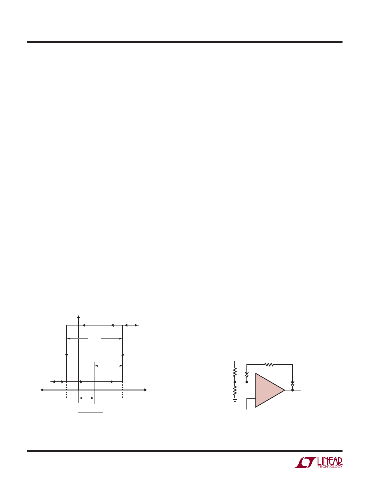
Hysteresis
The LT1715 includes internal hysteresis, which makes it
easier to use than many other similar speed comparators.
The input-output transfer characteristic is illustrated in
Figure 5 showing the defi nitions of V
and V
OS
HYST
based
upon the two measurable trip points. The hysteresis band
makes the LT1715 well behaved, even with slowly moving
inputs.
The exact amount of hysteresis will vary from part to part
as indicated in the specifi cations table. The hysteresis level
will also vary slightly with changes in supply voltage and
common mode voltage. A key advantage of the LT1715
is the signifi cant reduction in these effects, which is important whenever an LT1715 is used to detect a threshold
crossing in one direction only. In such a case, the relevant
trip point will be all that matters, and a stable offset voltage with an unpredictable level of hysteresis, as seen in
competing comparators, is useless. The LT1715 is many
times better than prior generation comparators in these
regards. In fact, the CMRR and PSRR tests are performed
by checking for changes in either trip point to the limits
indicated in the specifi cations table. Because the offset
voltage is the average of the trip points, the CMRR and
PSRR of the offset voltage is therefore guaranteed to be
at least as good as those limits. This more stringent test
also puts a limit on the common mode and power supply
dependence of the hysteresis voltage.
Additional hysteresis may be added externally. The railto-rail outputs of the LT1715 make this more predictable
than with TTL output comparators due to the LT1715’s
small variability of V
(output high voltage).
OH
To add additional hysteresis, set up positive feedback
by adding additional external resistor R3 as shown in
Figure 6. Resistor R3 adds a portion of the output to the
threshold set by the resistor string. The LT1715 pulls the
outputs to +V
and ground to within 200mV of the rails
S
with light loads, and to within 400mV with heavy loads.
For the load of most circuits, a good model for the voltage on the right side of R3 is 300mV or +V
for a total voltage swing of (+V
– 600mV.
+V
S
– 300mV) – (300mV) =
S
– 300mV,
S
With this in mind, calculation of the resistor values needed
is a two-step process. First, calculate the value of R3 based
on the additional hysteresis desired, the output voltage
swing and the impedance of the primary bias string:
12
OUT
V
V
HYST
+
– V
TRIP
TRIP
V
–
HYST
–
)
/2
V
TRIP
(= V
TRIP
V
OL
0
–
V
TRIP
V
+
V
+ V
TRIP
=
OS
2
Figure 5. Hysteresis I/O Characteristics
+
V
OH
ΔVIN = V
IN
1715 F05
+
– V
R3 = (R1||R2)(+V
– 0.6V)/(additional hysteresis)
S
Additional hysteresis is the desired overall hysteresis less
the internal 4mV hysteresis.
V
REF
R2
–
IN
R1
INPUT
Figure 6. Additional External Hysteresis
R3
+
1/2 LT1715
–
1715 F06
1715fa

APPLICATIONS INFORMATION
V
REF
R2´
V
TH
R1
Figure 7. Model for Additional Hysteresis Calculations
The second step is to recalculate R2 to set the same average threshold as before. The average threshold before
was set at V
TH
= (V
calculated based on the average output voltage (+V
the simplifi ed circuit model in Figure 7. To assure that the
comparator’s noninverting input is, on average, the same
as before:
V
TH
R2´ = (V
– VTH)/(VTH/R1 + (VTH – VS/2)/R3)
REF
For additional hysteresis of 10mV or less, it is not uncommon for R2´ to be the same as R2 within 1% resistor
tolerances.
This method will work for additional hysteresis of up to
a few hundred millivolts. Beyond that, the impedance of
R3 is low enough to effect the bias string, and adjustment of R1 may also be required. Note that the currents
through the R1/R2 bias string should be many times the
input currents of the LT1715. For 5% accuracy, the current must be at least 20 times the input current, more for
higher accuracy.
Interfacing the LT1715 to ECL
The LT1715’s comparators can be used in high speed applications where Emitter-Coupled Logic (ECL) is deployed.
To interface the output of the LT1715 to ECL logic inputs,
standard TTL/CMOS to ECL level translators such as the
10H124, 10H424 and 100124 can be used. The secomponents come at a cost of a few nanoseconds additional
delay as well as supply currents of 50mA or more, and
are only available in quads. A faster, simpler and lower
R3
+
1/2 LT1715
–
)(R1)/(R1 + R2). The new R2 is
REF
V
AVERAGE
=
1715 F07
+V
S
2
/2)and
S
LT1715
power translator can be constructed with resistors as
shown in Figure 8.
Figure 8a shows the standard TTL to Positive ECL (PECL)
resistive level translator. This translator cannot be used
forthe LT1715, or with CMOS logic, because it depends
on the 820Ω resistor to limit the output swing (V
the all-NPNTTL gate with its so-called totem-pole output.
The LT1715is fabricated in a complementary bipolar
process and the output stage has a PNP driver that pulls
the output nearly all the way to the supply rail, even when
sourcing 10mA.
Figure 8b shows a three resistor level translator for interfacing the LT1715 to ECL running off the same supply rail.
No pull-down on the output of the LT1715 is needed, but
pull-down R3 limits the V
seen by the PECL gate. This
IH
is needed because ECL inputs have both a minimum and
maximum V
specifi cation for proper operation. Resis-
IH
tor values are given for both ECL interface types; in both
cases it is assumed that the LT1715 operates from the
same supply rail.
Figure 8c shows the case of translating to PECL from
an LT1715 powered by a 3V supply rail. Again, resistor
values are given for both ECL interface types. This time
four resistors are needed, although with 10KH/E, R3 is not
needed. In that case, the circuit resembles the standard
TTL translator of Figure 8a, but the function of the new
resistor, R4, is much different. R4 loads the LT1715 output
when high so that the current fl owing through R1 doesn’t
forward bias the LT1715’s internal ESD clamp diode.
Although this diode can handle 20mA without damage,
normal operation and performance of the output stage can
be impaired above 100μA of forward current. R4 prevents
this with the minimum additional power dissipation.
Finally, Figure 8d shows the case of driving standard,
negative-rail, ECL with the LT1715. Resistor values are
given for both ECL interface types and for both a 5V
and 3V LT1715 supply rail. Again, a fourth resistor, R4
is needed to prevent the low state current from fl owing
out of the LT1715, turning on the internal ESD/substrate
diodes. Resistor R4 again prevents this with the minimum
additional power dissipation.
OH
) of
1715fa
13

LT1715
APPLICATIONS INFORMATION
Of course, if the VEE of the LT1715 is the same as the
ECL negative supply, the GND pin can be tied to it as well
and +V
grounded. Then the output stage has the same
S
powerrails as the ECL and the circuits of Figure 8b can
be used.
For all the dividers shown, the output impedance is about
110Ω. This makes these fast, less than a nanosecond,with
most layouts. Avoid the temptation to use speed up capaci-
5V
180Ω
LSTTL
(a) STANDARD TTL TO PECL TRANSLATOR
V
CC
1/2 LT1715
270Ω
820Ω
R1
5V
DO NOT USE FOR LT1715
10KH/E
+V
S
R2
R3
LEVEL TRANSLATION. SEE TEXT
10KH/E
100K/E
tors. Not only can they foul up the operation of the ECL
gate because of overshoots, they can damage the ECL
inputs, particularly during power-up of separate supply
confi gurations.
The level translator designs assume one gate load. Multiple
gates can have signifi cant I
loading, and the transmis-
IH
sion line routing and termination issues also make this
case diffi cult.
+V
5V OR 5.2V
4.5V
R1
R2
S
510Ω
620Ω
180Ω
180Ω
R3
750Ω
510Ω
V
EE
(b) LT1715 OUTPUT TO PECL TRANSLATOR
V
V
3V
CC
1/2 LT1715
V
EE
(c) 3V LT1715 OUTPUT TO PECL TRANSLATOR
+VSV
CC
1/2 LT1715
V
EE
(d) LT1715 OUTPUT TO STANDARD ECL TRANSLATOR
ECL
R2
R1
R3R4
R4
R1
R3
R2
V
ECL
10KH/E
100K/E
Figure 8
V
ECL
5V OR 5.2V
4.5V
ECL FAMILY
10KH/E
100K/E –4.5V
R1
300Ω
330Ω
V
ECL
–5.2V
R2
180Ω
180Ω
+V
5V
3V
5V
3V
S
R3
OMIT
1500Ω
R1
560Ω
270Ω
680Ω
330Ω
R4
560Ω
1000Ω
R2
270Ω
510Ω
270Ω
390Ω
R3
330Ω
300Ω
300Ω
270Ω
R4
1200Ω
330Ω
1500Ω
430Ω
1715 F08
1715fa
14

APPLICATIONS INFORMATION
LT1715
ECL, and particularly PECL, is valuable technology for high
speed system design, but it must be used with care. With
less than a volt of swing, the noise margins need to be
evaluated carefully. Note that there is some degradation of
noise margin due to the ±5% resistor selections shown.
With 10KH/E, there is no temperature compensation of
the logic levels, whereas the LT1715 and the circuits
shown give levels that are stable with temperature. This
will lower the noise margin over temperature. In some
confi gurations it is possible to add compensation with
diode or transistor junctions in series with the resistors
of these networks.
For more information on ECL design, refer to the ECLiPS
data book (DL140), the 10KH system design handbook
(HB205) and PECL design (AN1406), all from Motorola,
now ON Semiconductor.
Circuit Description
The block diagram of the LT1715 is shown in Figure 9.
The circuit topology consists of a differential input stage,
again stage with hysteresis and a complementary common-emitter output stage. All of the internal signal paths
utilize low voltage swings for high speed at low power.
The input stage topology maximizes the input dynamic
range available without requiring the power, complexity
and die area of two complete input stages such as are
found in rail-to-rail input comparators. With a single
2.7V supply, the LT1715 still has a respectable 1.6V of
input common mode range. The differential input voltage rangeis rail-to-rail, without the large input currents
found incompeting devices. The input stage also features
phase reversal protection to prevent false outputs when
the inputs are driven below the –100mV common mode
voltage limit.
The internal hysteresis is implemented by positive, nonlinear feedback around a second gain stage. Until this point,
the signal path has been entirely differential. The signal
path is then split into two drive signals for the upper and
lower output transistors. The output transistors are connected common emitter for rail-to-rail output operation.
The Schottky clamps limit the output voltages at about
300mV from the rail, not quite the 50mV or 15mV of Linear
Technology’s rail-to-rail amplifiers and other products. But
the output of a comparator is digital, and this output stage
can drive TTL or CMOS directly. It can also drive ECL, as
described earlier, or analog loads.
+IN
–IN
1715 F09
+V
OUT
GND
S
1715fa
NONLINEAR STAGE
+
V
CC
+
+
A
V1
–
V
EE
Σ
+
A
+
Σ
V2
–
Figure 9. LT1715 Block Diagram
–
+
–
15

LT1715
APPLICATIONS INFORMATION
The bias conditions and signal swings in the output stage
are designed to turn their respective output transistors off
faster than on. This helps minimize the surge of current
from +V
the frequency-dependent increase in power consumption.
The frequency dependence of the supply current is shown
in the Typical Performance Characteristics.
Speed Limits
The LT1715 comparator is intended for high speed applications, where it is important to understand a few
limitations. These limitations can roughly be divided into
three categories: input speed limits, output speed limits,
and internal speed limits.
There are no significant input speed limits except the shunt
capacitance of the input nodes. If the 2pF typical input
nodes are driven, the LT1715 will respond.
The output speed is constrained by three mechanisms, the
fi rst of which is the slew currents available from the output
transistors. To maintain low power quiescent operation,
the LT1715 output transistors are sized to deliver 35mA
to 60mA typical slew currents. This is sufficient to drive
small capacitive loads and logic gate inputs at extremely
high speeds. But the slew rate will slow dramatically with
heavy capacitive loads. Because the propagation delay (t
definition ends at the time the output voltage is halfway
between the supplies, the fixed slew current makes the
LT1715 faster at 3V than 5V with large capacitive loads
and suffi cient input overdrive.
Another manifestation of this output speed limit is skew,
the difference between t
of the LT1715 vary with the process variations of the PNP
and NPN transistors, for rising edges and falling edges
respectively. The typical 0.5ns skew can have either polarity, rising edge or falling edge faster. Again, the skew will
increase dramatically with heavy capacitive loads.
A fi nal limit to output speed is the turn-on and turn-off
time of the output devices. Each device has substantial
to ground that occurs at transitions, to minimize
S
PD
PD
+
and t
–
. The slew currents
PD
)
base charge that requires one nanosecond or more of
active charging or discharging by the bias current of
the Darlington driver stage. When toggle rates are high
enough that insuffi cient time is allowed for this turn-on
or turn-off, glitches may occur leading to dropout or runt
pulses. Furthermore, power consumption may increase
nonlinearly if devices are not turned off before the opposing cycle. However, once the toggle frequency increases
or decreases, the part will easily leave this undesired
operating mode no worse for the wear provided there
is adequate heat sinking toprevent thermal overload. At
frequencies well beyond the maximum toggle rate, the part
will toggle with limited output swing and well controlled
power consumption.
The internal speed limits manifest themselves as dispersion. All comparators have some degree of dispersion,
defined as a change in propagation delay versus input
overdrive. The propagation delay of the LT1715 will vary
with overdrive, from a typical of 4ns at 20mV overdrive
to 6ns at 5mV overdrive (typical). The LT1715’s primary
source of dispersion is the hysteresis stage. As a change
of polarity arrives at the gain stage, the positive feedback
of the hysteresis stage subtracts from the overdrive available. Only when enough time has elapsed for a signal to
propagate forward through the gain stage, backwards
through the hysteresis path and forward through the gain
stage again, will the output stage receive the same level
of overdrive that it would have received in the absence of
hysteresis.
The LT1715 is several hundred picoseconds faster when
= –5V, relative to single supply operation. This is due
V
EE
to the internal speed limit; the gain stage operates between
and +VS, and it is faster with higher reverse voltage
V
EE
bias due to reduced silicon junction capacitances.
In many applications, as shown in the following examples,
there is plenty of input overdrive. Even in applications providing low levels of overdrive, the LT1715 is fast enough
that the absolute dispersion of 2ns (= 6 – 4) is often small
enough to ignore.
16
1715fa

APPLICATIONS INFORMATION
LT1715
The gain and hysteresis stage of the LT1715 is simple, short
and high speed to help prevent parasitic oscillations while
adding minimum dispersion. This internal “self-latch” can
be usefully exploited in many applications because it occurs
early in the signal chain, in a low power, fully differential
stage. It is therefore highly immune to disturbances from
other parts of the circuit, such as the output, or on the
supply lines. Once a high speed signal trips the hysteresis,
the output will respond, after some propagation delay,
without regard to these external influences that can cause
trouble in nonhysteretic comparators.
Test Circuit
±V
TRIP
The input trip points test circuit uses a 1kHz triangle wave
to repeatedly trip the comparator being tested. The LT1715
output is used to trigger switched capacitor sampling of
the triangle wave, with a sampler for each direction.
Because the triangle wave is attenuated 1000:1 and fed to
the LT1715’s differential input, the sampled voltages are
therefore 1000 times the input trip voltages. The hysteresis
and offset are computed from the trip points as shown.
1715fa
17


PACKAGE DESCRIPTION
LT1715
MS Package
10-Lead Plastic MSOP
(Reference LTC DWG # 05-08-1661)
0.889 ± 0.127
(.035 ± .005)
5.23
(.206)
MIN
0.305 ± 0.038
(.0120 ± .0015)
TYP
RECOMMENDED SOLDER PAD LAYOUT
0.254
(.010)
GAUGE PLANE
0.18
(.007)
NOTE:
1. DIMENSIONS IN MILLIMETER/(INCH)
2. DRAWING NOT TO SCALE
3. DIMENSION DOES NOT INCLUDE MOLD FLASH, PROTRUSIONS OR GATE BURRS.
MOLD FLASH, PROTRUSIONS OR GATE BURRS SHALL NOT EXCEED 0.152mm (.006") PER SIDE
4. DIMENSION DOES NOT INCLUDE INTERLEAD FLASH OR PROTRUSIONS.
INTERLEAD FLASH OR PROTRUSIONS SHALL NOT EXCEED 0.152mm (.006") PER SIDE
5. LEAD COPLANARITY (BOTTOM OF LEADS AFTER FORMING) SHALL BE 0.102mm (.004") MAX
3.20 – 3.45
(.126 – .136)
DETAIL “A”
DETAIL “A”
0.50
(.0197)
BSC
0° – 6° TYP
0.53 ± 0.152
(.021 ± .006)
SEATING
PLANE
3.00 ± 0.102
(.118 ± .004)
(NOTE 3)
4.90 ± 0.152
(.193 ± .006)
1.10
(.043)
MAX
0.17 – 0.27
(.007 – .011)
TYP
12
0.50
(.0197)
BSC
0.497 ± 0.076
6
45
(.0196 ± .003)
REF
3.00 ± 0.102
(.118 ± .004)
(NOTE 4)
0.86
(.034)
REF
0.1016 ± 0.0508
(.004 ± .002)
MSOP (MS) 0307 REV E
8910
7
3
Information furnished by Linear Technology Corporation is believed to be accurate and reliable.
However, no responsibility is assumed for its use. Linear Technology Corporation makes no representation that the interconnection of its circuits as described herein will not infringe on existing patent rights.
1715fa
19

LT1715
TYPICAL APPLICATION
High Performance Sine Wave
to Square Wave Converter
Propagation delay of comparators is typically specifi ed fora
100mV step with some fraction of that for overdrive. But
in many signal processing applications, such as in communications, the goal is to convert a sine wave, such as
a carrier, to a square wave for use as a timing clock. The
desired behavior is for the output timing to be dependent
on the input timing only. No phase shift should occur as
a function of the input amplitude, which would result in
AM to FM conversion.
The circuit of Figure 12a is a simple LT1715-based sine
wave to square wave converter. The ±5V supplies on the
input allow very large swing inputs, while the 3V logic
supply keeps the output swing small to minimize crosstalk.
Figure 12b shows the time delay vs input amplitude with a
10MHz sine wave. The LT1715 delay changes just 0.65ns
over the 26dB amplitude range; 2.33° at 10MHz. The delay
is particularly fl at yielding excellent AM rejection from 0dBm
to 15dBm. If a 2:1 transformer is used to drive the input
differentially, this exceptionally fl at zone spans –5dBm to
10dBm, a common range for RF signal levels.
5V
+
1/2 LT1715
–
–5V
3V
SQUARE WAVE
OUTPUT
1715 F12a
SINE WAVE
INPUT
50Ω
Similar delay performance is achieved with input frequencies as high as 50MHz. There is, however, some
additional encroachment into the central fl at zone by both
the small amplitude and large amplitude variations. With
small input signals, the hysteresis and dispersion make
the LT1715 act like a comparator with a 12mV hysteresis
span. In other words, a 12mV
sine wave at 10MHz will
P-P
barely toggle the LT1715, with 90° of phase lagor 25ns
additional delay.
Above 5V
at 10MHz, the LT1715 delay starts to decrease
P-P
due to internal capacitive feed-forward in the input stage.
Unlike some comparators, the LT1715 will not falsely anticipate a change in input polarity, but the feed-forward is
enough to make a transition propagate through the LT1715
faster once the input polarity does change.
5
4
25°C
= 5V
V
CC
= –5V
V
3
EE
= 3V
+V
S
10MHz
2
TIME DELAY (ns)
1
632mV
0
–5
0
2V
P-P
INPUT AMPLITUDE (dBm)
P-P
51015
6.32V
20 25
P-P
1715 F12b
Figure 12a. LT1715-Based Sine Wave to Square Wave Converter Figure 12b. Time Delay vs Sine Wave Input Amplitude
RELATED PARTS
PART NUMBER DESCRIPTION COMMENTS
LT1016 UltraFast Precision Comparator Industry Standard 10ns Comparator
LT1116 12ns Single Supply Ground-Sensing Comparator Single Supply Version of LT1016
LT1394 7ns, UltraFast, Single Supply Comparator 6mA Single Supply Comparator
LT1711/LT1712 4.5ns, 3V/5V/±5V Single/Dual Rail-to-Rail Comparators UltraFast Rail-to-Rail Input and Output Comparator
LT1713/LT1714 7ns, Low Power, 3V/5V/±5V Single/Dual Rail-to-Rail Comparators Rail-to-Rail Input and Output Comparator
LT1719 4.5ns Single Supply 3V/5V Comparator Single Comparator Similar to the LT1715
LT1720/LT1721 Dual/Quad 4.5ns, Single Supply 3V/5V Comparator Dual/Quad Comparator Similar to the LT1715
LT 1008 REV A • PRINTED IN USA
20
Linear Technology Corporation
1630 McCarthy Blvd., Milpitas, CA 95035-7417
(408) 432-1900 ● FAX: (408) 434-0507
●
www.linear.com
© LINEAR TECHNOLOGY CORPORATION 2001
1715fa
 Loading...