

Linear Technology LT1684 Datasheet
FEATURES
■
Allows Dynamic Control of Output Frequency,
Cadence, Amplitude and DC Offset
■
Active Tracking Supply Configuration Allows Linear
Generation of Ring Tone Signal
■
No High Voltage Post-Filtering Required
■
Capacitive Isolation Eliminates Optocouplers
■
Low Distortion Output Meets International
PTT Requirements
■
Differential Input Signal for Noise Immunity
■
User Adjustable Active Output Current Limit
■
Powered Directly From High Voltage Ringer
Supply—No Additional Supplies Necessary
■
Supply Current: <1mA
■
2% Signal Amplitude Reference
■
Available in 14-Pin SO and DIP Packages
U
APPLICATIO S
■
Wireless Local Loop Telephones
■
Key System/PBX Equipment
■
Fiber to the Curb Telecom Equipment
LT1684
Micropower
Ring Tone Generator
U
DESCRIPTIO
The LT®1684 is a telecommunication ring tone generator.
The IC takes a user-generated pulse width modulated
(PWM) input and converts it to a high voltage sine wave
suitable for telephone ringing applications.
The LT1684 receives capacitor-isolated differential PWM
input signals encoded with desired ring output cadence,
frequency, and amplitude information. The LT1684 normalizes the pulse amplitude to ±1.25V for an accurate
signal voltage reference. The cadence, frequency and
amplitude information is extracted using a multiplepole active filter/amplifier, producing the output ring tone
signal.
The LT1684 uses its own ring tone output as a reference
for generating local supply rails using complementary
high voltage external MOSFETs as dynamic level-shifting
devices. This “active tracking” supply mode of operation
allows linear generation of the high voltage ring tone
signal, reducing the need for large high voltage filtering
elements.
, LTC and LT are registered trademarks of Linear Technology Corporation.
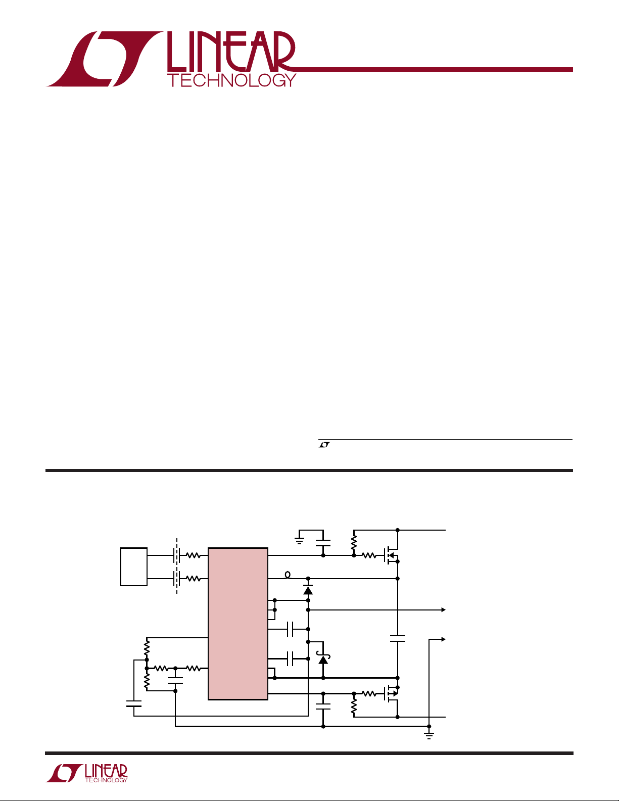
TYPICAL APPLICATIO
1µF
ISOLATION
100pF
100pF
3k
2k
300k
DC
10k
10k
4700pF
PWM
CONTROLLER
P1
µC
P2
FB1: FERRONICS FMB1601 (716) 388-1020
U
5k
Electrically Isolated Ring Tone Generator
6.8nF
1N4001
1N5817
6.8nF
IN A GATE
IN B
LT1684
LIM
OUT
OUT
AT
COMP1
COMP2
GATE
BG
AMPIN LIM
REF
+
FB1
+
V
+
100pF
20pF
–
–
V
–
100k
100Ω
100Ω
100k
IRF610
0.1µF
IRF9610
100V
+
RING TONE
OUTPUT
–
–100V
1684 TA01
±100mA
()
CAPABILITY
1

LT1684
WWWU
ABSOLUTE AXI U RATI GS
(Note 1)
Voltages:
Active Tracking Differential Voltage
(GATE+ – GATE–)..................................–0.3V to 42V
Local Supply Differential Voltage
(V+ – V–)...............................................–0.3V to 36V
Local Supply
Voltage V
+
..............
(GATE+ – 7.0V) to (GATE+ + 0.3V)
Local Supply
Voltage V
–
..............
(GATE– – 0.3V) to (GATE– + 7.0V)
PWM Input Differential Voltage
(IN A – IN B).........................................–7.0V to 7.0V
PWM Input Voltage
Common Mode................. (V– – 0.3V) to (V+ + 0.3V)
LIM+ Current Limit
Pin Voltage ..................... (OUT – 0.3V) to (V+ + 0.3V)
LIM– Current Limit
Pin Voltage .................... (V– – 0.3V) to (OUT + 0.3V)
All Other Pin Voltages ........... (V– – 0.3V) to (V+ + 0.3V)
UU
W
PACKAGE/ORDER I FOR ATIO
Currents:
LIM+, LIM– Current.......................................... –350mA
OUT Current ....................................................... 350mA
BG
Current .................................................... ±10mA
OUT
PWM (IN A, IN B) Current .................................... ±5mA
GATE+, GATE– Current .......................................±20mA
COMP1 Current .................................................... ±1mA
COMP2 Current .................................................... ±1mA
AT
Current ..................................................... ±20mA
REF
Temperatures:
Operating Junction Temperature Range
Commercial Grade................................. 0°C to 125°C
Industrial Grade................................ –40°C to 125°C
Storage Temperature Range ................. –65°C to 150°C
Lead Temperature (Soldering, 10 sec)..................300°C
TOP VIEW
1
IN B
2
COMP1
3
COMP2
–
4
LIM
–
5
V
–
6
GATE
7
AT
REF
N PACKAGE
14-LEAD PDIP
T
= 125°C, θ
JMAX
= 125°C, θ
T
JMAX
Consult factory for Military grade parts.
JA
JA
IN A
14
BG
13
OUT
AMPIN
12
+
GATE
11
+
V
10
+
LIM
9
OUT
8
S PACKAGE
14-LEAD PLASTIC SO
= 75°C/W (N)
= 115°C/W (S)
ORDER PART
NUMBER
LT1684CN
LT1684CS
LT1684IN
LT1684IS
2
LT1684
ELECTRICAL CHARACTERISTICS
The ● denotes the specifications which apply over the full operating temperature range, otherwise specifications are at TA = 25°C.
V+ – V– = 20V, Voltages referenced to pin OUT, V
SYMBOL PARAMETER CONDITIONS MIN TYP MAX UNITS
Supply and Protection
I
S
|V+| Local Supply Voltages V
|V–|V
V
GATE
V
GATE
PWM Receiver
f
PWM
V
IN
R
IN
R
INA,INB
BG Buffer
V
BGOUT
V
BGOUTOS
I
BGOUTSC
R
BGOUT
t
r
t
f
∆t
r-f
t
pr
t
pf
∆t
p
Output Amplifier
V
OUTOS
R
OUT
I
OUTSC
DC Supply Current (Note 2) IN A – IN B ≥ 1.6V ● 680 950 µA
+ Active Tracking Supply FET I
Bias Voltage AT
– Active Tracking Supply FET I
Bias Voltage AT
Input Carrier Frequency 10 kHz
Minimum Valid Differential Input IN A – IN B or IN B – IN A ● 1.6 V
Differential Input Threshold ● 0.50 0.70 1.00 V
| IN A – IN B |
Differential Input Overdrive Impedance VIN > VTH + 100mV ● 710 kΩ
(Note 3, 5)
Single-Ended Input Impedance To Pin OUT ● 50 kΩ
(Note 5)
BG
Normalized Voltage Magnitude |V
OUT
Output Offset Voltage –7 7 mV
[(V
+) + (V
BGOUT
BG
Short-Circuit Current ● ±2 ±4.5 mA
OUT
BG
Output Impedance –2mA ≤ I
OUT
BG
Rise Time (10% to 90%) R
OUT
BG
Fall Time (10% to 90%) R
OUT
BG
RiseTime – Fall Time ● –200 –100 0 ns
OUT
BG
Propagation Delay PWM Input R
OUT
–)]/2 ● –10 10 mV
BGOUT
Transition to 10% Output (Rising Edge)
BG
Propagation Delay PWM Input R
OUT
Transition to 90% Output (Falling Edge)
BG
Propagation Delay ● – 200 –100 100 ns
OUT
Rising Edge – Falling Edge
OUT Offset Voltage V
OUT Output Impedance –10mA ≥ I
OUT Short-Circuit Current LIM+ Shorted to OUT ● ±100 ±190 mA
= V
OUT
GATE
GATE
+ = –100µA, ● 13.2 14.0 14.8 V
GATE
REF
– = 100µA, ● –14.8 –14.0 –13.2 V
GATE
REF
= 5k, C
OUT
= 5k, C
OUT
= 5k, C
OUT
= 5k, C
OUT
AMPIN
R
AMPIN
10mA ≤ I
LIM– Shorted to V
unless otherwise noted.
ATREF
+
+ ≥ V
– ≤ V
–
● 6.5 10 V
= 0V
= 0V
| 1.235 1.250 1.265 V
BGOUT
≤ 2mA 0.2 Ω
BGOUT
= 10pF ● 160 300 ns
OUT
= 10pF ● 260 400 ns
OUT
= 10pF ● 340 500 ns
OUT
= 10pF ● 440 600 ns
OUT
= 0v, I
= 0A – 6 6 mV
OUT
● 1.225 1.250 1.275 V
= 10k (Note 4) ● –8 8 mV
+ ≥ –100mA, LIM+ Shorted to OUT 0.01 Ω
LIM
≤ 100mA, LIM– Shorted to V
OUT
–
–
0.15 Ω
Note 1: Absolute Maximum Ratings are those values beyond which the life
of the device may be impaired.
Note 2: IC Supply current specification represents unloaded condition and
does not include external FET gate pull up/down currents (GATE
+
, GATE
–
pins). Actual total IC bias currents will be higher and vary with operating
conditions. See Applications Information.
Note 3: PWM inputs are high impedance through ±100mV beyond the
input thresholds.
Note 4: 10k resistor from pin AMPIN to ground.
Note 5: Guaranteed but not tested.
3
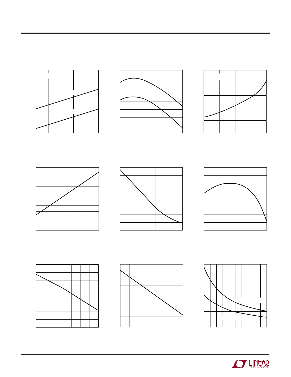
LT1684
I
GATE
(mA)
0.1 0.3 1.0 3.0 10.0
V
GATE
– V
ATREF
(V)
1684 G03
14.3
14.2
14.1
14.0
13.9
13.8
TJ = 25°C
TEMPERATURE (°C)
–50 –25 0 25 50 75 100 125
V
BGOUT
(V)
1684 G06
1.253
1.252
1.251
1.250
1.249
1.248
1.247
1.246
1.245
R
LIM
(Ω)
0 21 4 6 83 5 7 910
OUTPUT CURRENT LIMIT (mA)
1684 G09
200
150
100
50
0
TYPICAL (TJ = 25°C)
MINIMUM (TJ = 125°C)
UW
TYPICAL PERFOR A CE CHARACTERISTICS
DC Supply Current vs V+ – V
740
TJ = 25°C
720
700
680
660
640
DC SUPPLY CURRENT (µA)
620
600
14 16 18 20 22 24
V
GATE
IN A – IN B ≥ 1.6V
IN A – IN B ≤ –1.6V
– V
ATREF
V+ – V– (V)
Voltage
Magnitudes vs Temperature
14.5
I
= 1mA
GATE
14.4
14.3
14.2
(V)
14.1
ATREF
14.0
– V
13.9
GATE
13.8
V
13.7
13.6
13.5
–50 –25 0 25 50 75 100 125
TEMPERATURE (°C)
–
1684 G01
DC Supply Current vs Temperature
710
690
670
650
630
IN A – IN B ≤ –1.6V
610
590
DC SUPPLY CURRENT (µA)
570
550
–50 –25 0 25 50 75 100 125
TEMPERATURE (°C)
IN A – IN B ≥ 1.6V
PWM Input Thresholds vs
Temperature V
0.85
0.80
0.75
0.70
0.65
0.60
IN A – IN B (V)
0.55
0.50
0.45
–50 –25 0 25 50 75 100 125
1684 G04
TEMPERATURE (°C)
1684 G02
1684 G05
V
– V
GATE
Magnitudes vs I
BGOUT
Voltage
ATREF
GATE
Magnitude vs Temperature
PWM Buffer (Pin BG
Limit vs Temperature
6.0
5.5
5.0
4.5
4.0
3.5
3.0
2.5
PWM BUFFER CURRENT LIMIT (mA)
2.0
–50 –25 0 25 50 75 100 125
TEMPERATURE (°C)
4
OUT
) Current
1684 G07
Output Amplifier Current Limit vs
Temperature (R
250
225
200
175
150
OUTPUT CURRENT LIMIT (mA)
125
100
–50 –25 0 25 50 75 100 125
TEMPERATURE (°C)
LIM
= 0Ω)
Output Amplifier Current Limit vs
External Limiting Resistor Values
1684 G08

LT1684
U
UU
PI FU CTIO S
IN B (Pin 1): PWM Negative Input. Input is isolated from
digital source by ~100pF series capacitor. A 10k resistor
can be connected to the IN B pin in series with the isolation
capacitor for transient protection. The PWM receiver implements a diode forward drop of input hysteresis (relative to
IN A). This hysteresis and internal signal limiting assure
common mode glitch rejection with isolation capacitor
mismatches up to 2:1. For maximum performance, however, effort should be made to match the two PWM input
isolation capacitors. Pin IN B is differentially clamped to
pin IN A through back-to-back diodes. This results in a
high impedance differential input through ±100mV beyond the input thresholds. 5k internal input resistors yield
a 10k (nominal) differential overdrive impedance.
COMP1 (Pin 2): Output Amplifier Primary Compensation.
Connect a 100pF capacitor from pin COMP1 to pin OUT.
COMP2 (Pin 3): Output Amplifier Secondary Compensation. Connect a 20pF capacitor from pin COMP2 to pin
OUT.
LIM– (Pin 4): Output Amplifier Current Sink Limit. Pin
implements I
resistor has a typical value of 3.5Ω. For maximum current
drive capability (190mA typical) short pin to pin V–.
Reduction of current sink capability is achieved by placing
additional resistance from pin LIM– to pin V–. (i.e. An
external 3.5Ω resistance from pin LIM– to pin V– will
reduce the current sinking capability of the output amplifier by approximately 50%.)
V– (Pin 5): Local Negative Supply. Typically connected to
the source of the active tracking supply P-channel MOSFET.
V– rail voltage is GATE– self-bias voltage less the MOSFET
VGS. Typical P-channel MOSFET characteristics provide
AT
– V– ≈ 10V.
REF
GATE– (Pin 6): Negative Power Supply FET Gate Drive. Pin
sources current from pull-down resistor to bias gate of
active tracking supply P-channel MOSFET. Self-biases to
a typical value of –14V, referenced to pin AT
resistor value is determined such that current sourced
from the GATE– pin remains greater than 50µA at mini-
mum output signal voltage and less than 10mA at maximum output signal voltage.
• R = VBE current clamp. Internal clamp
OUT
. Pull-down
REF
AT
(Pin 7): Active Tracking Supply Reference. Typi-
REF
cally connected to pin OUT. Pin bias current is the difference between the magnitudes of GATE+ pin bias and
GATE– pin bias (I
OUT (Pin 8): Ring Tone Output Pin. Output of active filter
amplifier/buffer. Used as reference voltage for internal
functions of IC. Usually shorted to pin AT
reference for active tracking supply circuitry. Connect a 1A
(1N4001-type) diode between V+ and OUT and a
1A Schottky diode from V– to OUT for line transient
protection.
LIM+ (Pin 9): Output Amplifier Current Source Limit. Pin
implements I
resistor has a typical value of 3.5Ω. For maximum current
drive capability (190mA typical) short pin LIM+ to pin
OUT. Reduction of current source capability is achieved by
placing additional resistance from pin LIM+ to pin OUT.
(i.e. An external 3.5Ω resistance from pin LIM+ to pin OUT
will reduce the current sourcing capability of the output
amplifier by approximately 50%.)
V+ (Pin 10): Local Positive Supply. Typically connected to
the source of the active tracking supply N-channel MOSFET.
This condition should be made using a ferrite bead.
Operating V+ rail voltage is GATE+ self-bias voltage less
the MOSFET VGS. Typical N-channel MOSFET characteristics provide V+ – AT
GATE+ (Pin 11): Positive Power Supply FET Gate Drive.
Pin sinks current from pull-up resistor to bias gate of
active tracking supply N-channel MOSFET. Self-biases to
a typical value of 14V, referenced to pin AT
resistor value is determined such that sink current into
GATE+ pin remains greater than 50µA at maximum output
signal voltage and less than 10mA at minimum output
signal voltage.
AMPIN (Pin 12): Output Amplifier Input. Connected to
external filter components through series protection resistor (usually 5k). Thevenin DC resistance of external
filter and protection components should be 10k for optimum amplifier offset performance. See Applications Information section.
OUT
= I
ATREF
• R = VBE current clamp. Internal clamp
≈ 10V.
REF
GATE
+ – I
–).
GATE
to generate
REF
REF
. Pull-up
5
 Loading...