

FEATURES
■
Rail-to-Rail Input and Output
■
100% Tested Low Voltage Noise:
3.2nV/√Hz Typ at 1kHz
4.5nV/√Hz Max at 1kHz
■
Offset Voltage: 60µV Max
■
Low VOS Drift: 0.2µV/°C Typ
■
Low Input Bias Current: 20nA Max
■
Wide Supply Range: 3V to ±18V
■
High A
■
High CMRR: 109dB Min
■
High PSRR: 108dB Min
■
Gain Bandwidth Product: 7.2MHz
■
Slew Rate: 2.5V/µs
■
Operating Temperature Range: –40°C to 85°C
: 7V/µV Min, RL = 10k
VOL
U
APPLICATIO S
■
Low Noise Signal Processing
■
Microvolt Accuracy Threshold Detection
■
Strain Gauge Amplifiers
■
Tape Head Preamplifiers
■
Direct Coupled Audio Gain Stages
■
Infrared Detectors
■
Battery-Powered Microphones
LT1677
Low Noise, Rail-to-Rail
Precision Op Amp
U
DESCRIPTIO
The LT®1677 features the lowest noise performance available for a rail-to-rail operational amplifier: 3.2nV/√Hz
wideband noise, 1/f corner frequency of 13Hz and 90nV
peak-to-peak 0.1Hz to 10Hz noise. Low noise is combined
with outstanding precision: 20µV offset voltage and
0.2µV/°C drift, 130dB common mode and power supply
rejection and 7.2MHz gain bandwidth product. The common mode range exceeds the power supply by 100mV.
The voltage gain of the LT1677 is extremely high, 19 million
(typical) driving a 10k load.
In the design, processing and testing of the device, particular
attention has been paid to the optimization of the entire
distribution of several key parameters. Consequently, the
specifications have been spectacularly improved compared
to competing rail-to-rail amplifiers.
, LT, LTC and LTM are registered trademarks of Linear Technology Corporation.
All other trademarks are the property of their respective owners.
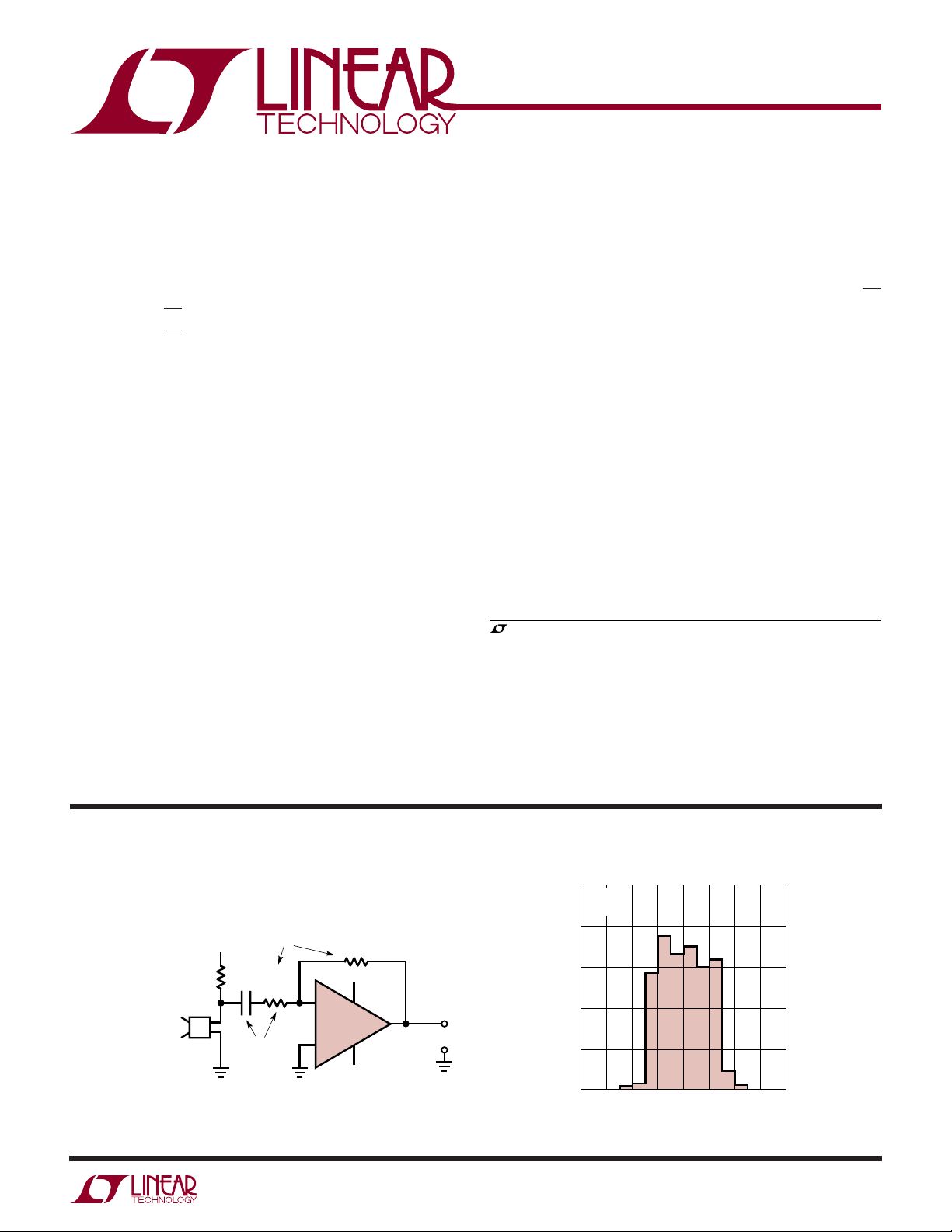
TYPICAL APPLICATIO
3V Electret Microphone Amplifier
= –100
A
PANASONIC
ELECTRET
CONDENSER
MICROPHONE
WM-61
www.panasonic.com/pic
(714) 373-7334
1.5V
R1
10k
C1
0.68µF
23Hz
HIGHPASS
V
R2
10k
U
Distribution of Offset Voltage
25
TA = 25°C
= ±15V
V
S
R3
1M
1.5V
–
2
3
LT1677
+
7
4
–1.5V
HEADPHONES
6
1677 TA01
TO PA
OR
20
15
10
PERCENT OF UNITS
5
0
–40
–30 –20
INPUT OFFSET VOLTAGE (µV)
0
–10 10 40
20 30
1677 TA02
1677fa
1
LT1677
TOP VIEW
S8 PACKAGE
8-LEAD PLASTIC SO
N8 PACKAGE
8-LEAD PDIP
1
2
3
4
8
7
6
5
V
OS
TRIM
V
OS
TRIM
+V
S
OUT
NC
–IN
+IN
–V
S
–
+
WWWU
ABSOLUTE AXI U RATI GS
PACKAGE/ORDER I FOR ATIO
UU
W
(Note 1)
Supply Voltage ...................................................... ± 22V
Input Voltages (Note 2) ............ 0.3V Beyond Either Rail
Differential Input Current (Note 2) ..................... ± 25mA
Output Short-Circuit Duration (Note 3) ............ Indefinite
Storage Temperature Range ................. –65°C to 150°C
T
= 150°C, θJA = 150°C/ W (N8)
Lead Temperature (Soldering, 10 sec.).................300°C
Operating Temperature Range
LT1677C (Note 4) ............................. – 40°C to 85°C
LT1677I ............................................. – 40°C to 85°C
Specified Temperature Range
LT1677C (Note 5) ............................. – 40°C to 85°C
LT1677I ............................................. – 40°C to 85°C
ELECTRICAL CHARACTERISTICS
temperature range, otherwise specifications are at T
SYMBOL PARAMETER CONDITIONS (Note 6) MIN TYP MAX UNITS
V
OS
∆V
∆Temp
∆V
∆Time
I
B
I
OS
2
OS
OS
Input Offset Voltage (Note 11) 35 90 µV
Average Input Offset Drift (Note 10) SO-8
Long Term Input Voltage Stability 0.3 µV/Mo
Input Bias Current (Note 11) ±2 ±20 nA
Input Offset Current (Note 11) 415 nA
= 25°C. VS = 3V, VCM = VO = 1.7V; VS = 5V, VCM = VO = 2.5V unless otherwise noted.
A
The ● denotes the specifications which apply over the full operating
≤ 70°C
0°C ≤ T
A
–40°C ≤ T
VCM = VS + 0.1V 150 400 µV
= VS – 0.2V, 0°C ≤ TA ≤ 70°C
V
CM
= VS – 0.3V, –40°C ≤ TA ≤ 85°C
V
CM
VCM = –0.1V 1.5 5.0 mV
= 0V, 0°C ≤ TA ≤ 70°C
V
CM
= 0V, –40°C ≤ TA ≤ 85°C
V
CM
N8
0°C ≤ TA ≤ 70°C
–40°C ≤ T
VCM = VS + 0.1V 0.19 0.40 µA
= VS – 0.2V, 0°C ≤ TA ≤ 70°C
V
CM
= VS – 0.3V, –40°C ≤ TA ≤ 85°C
V
CM
VCM = –0.1V –1.2 –0.41 µA
= 0V, 0°C ≤ TA ≤ 70°C
V
CM
= 0V, –40°C ≤ TA ≤ 85°C
V
CM
≤ 70°C
0°C ≤ T
A
–40°C ≤ T
VCM = VS + 0.1V 6 30 nA
= VS – 0.2V, 0°C ≤ TA ≤ 70°C
V
CM
= VS – 0.3V, –40°C ≤ TA ≤ 85°C
V
CM
VCM = –0.1V 20 100 nA
= 0V, 0°C ≤ TA ≤ 70°C
V
CM
VCM = 0V, –40°C ≤ TA ≤ 85°C
ORDER PART NUMBER
LT1677CS8
LT1677IS8
LT1677CN8
LT1677IN8
Order Options Tape and Reel: Add #TR
Lead Free: Add #PBF Lead Free Tape and Reel: Add #TRPBF
Lead Free Part Marking: http://www.linear.com/leadfree/
Consult LTC Marketing for parts specified with wider operating temperature ranges.
≤ 85°C
A
≤ 85°C
A
≤ 85°C
A
JMAX
= 150°C, θJA = 190°C/ W (S0-8)
T
JMAX
●
●
●
●
●
●
●
●
●
●
●
●
●
–2.0 – 0.45 µA
●
–2.3 – 0.47 µA
●
●
●
●
●
●
S8 PART MARKING
1677
1677I
55 150 µV
75 210 µV
180 550 µV
200 650 µV
1.8 6.0 mV
2.0 6.5 mV
0.40 2.0 µV/°C
0.20 1.5 µV/°C
±3 ±35 nA
±7 ±50 nA
0.19 0.60 µA
0.25 0.75 µA
520 nA
840 nA
10 40 nA
15 65 nA
25 150 nA
30 160 nA
1677fa

LT1677
ELECTRICAL CHARACTERISTICS
temperature range, otherwise specifications are at T
The ● denotes the specifications which apply over the full operating
= 25°C. VS = 3V, VCM = VO = 1.7V; VS = 5V, VCM = VO = 2.5V unless
A
otherwise noted.
SYMBOL PARAMETER CONDITIONS (Note 6) MIN TYP MAX UNITS
e
n
i
n
V
CM
R
IN
C
IN
CMRR Common Mode Rejection Ratio (Note 11) VS = 3V
PSRR Power Supply Rejection Ratio VS = 2.7V to 40V, VCM = VO = 1.7V 108 125 dB
A
VOL
Input Noise Voltage 0.1Hz to 10Hz (Note 7) 90 nV
VCM = V
S
180 nV
VCM = 0V 600 nV
P-P
P-P
P-P
Input Noise Voltage Density (Note 8) fO = 10Hz 5.2 nV/√Hz
= VS, fO = 10Hz 7 nV/√Hz
V
CM
= 0V, fO = 10Hz 25 nV/√Hz
V
CM
fO = 1kHz 3.2 4.5 nV/√Hz
V
= VS, fO = 1kHz 5.3 nV/√Hz
CM
= 0V, fO = 1kHz 17 nV/√Hz
V
CM
Input Noise Current Density fO = 10Hz 1.2 pA/√Hz
= 1kHz 0.3 pA/√Hz
f
O
Input Voltage Range –0.1 VS + 0.1V V
0°C ≤ T
A
–40°C ≤ T
≤ 70°C
≤ 85°C
A
●
0V
●
0V
S
S
– 0.2V V
– 0.3V V
Input Resistance Common Mode 2 GΩ
Input Capacitance 4.2 pF
V
= –0.1V to 3.1V 55 68 dB
CM
= 0V to 2.7V
V
CM
●
53 67 dB
VS = 5V
= –0.1V to 5.1V 60 73 dB
V
CM
V
= 0V to 4.7V
CM
= 3.1V to 40V, VCM = VO = 1.7V
V
S
●
58 72 dB
●
105 120 dB
Large-Signal Voltage Gain VS = 3V, RL ≥ 10k, VO = 2.5V to 0.7V 0.6 4 V/µV
0°C ≤ T
A
–40°C ≤ T
≤ 70°C
≤ 85°C
A
●
0.4 3 V/µV
●
0.4 3 V/µV
VS = 3V, RL ≥ 2k, VO = 2.2V to 0.7V 0.5 1 V/µV
0°C ≤ T
A
–40°C ≤ T
≤ 70°C
≤ 85°C
A
●
0.4 0.9 V/µV
●
0.4 0.8 V/µV
VS = 3V, RL ≥ 600Ω, VO = 2.2V to 0.7V 0.20 0.43 V/µV
0°C ≤ T
A
–40°C ≤ T
≤ 70°C
≤ 85°C
A
●
0.15 0.40 V/µV
●
0.10 0.35 V/µV
VS = 5V, RL ≥ 10k, VO = 4.5V to 0.7V 0.8 5 V/µV
0°C ≤ T
A
–40°C ≤ T
≤ 70°C
≤ 85°C
A
●
0.7 4 V/µV
●
0.7 4 V/µV
VS = 5V, RL ≥ 2k, VO = 4.2V to 0.7V 0.40 0.9 V/µV
0°C ≤ T
A
–40°C ≤ T
≤ 70°C
≤ 85°C
A
●
0.35 0.8 V/µV
●
0.25 0.6 V/µV
VS = 5V, RL ≥ 600Ω, VO = 4.2V to 0.7V 0.35 0.67 V/µV
0°C ≤ T
A
–40°C ≤ T
≤ 70°C
≤ 85°C
A
●
0.30 0.60 V/µV
●
0.20 0.45 V/µV
1677fa
3
LT1677
ELECTRICAL CHARACTERISTICS
temperature range, otherwise specifications are at T
The ● denotes the specifications which apply over the full operating
= 25°C. VS = 3V, VCM = VO = 1.7V; VS = 5V, VCM = VO = 2.5V unless
A
otherwise noted.
SYMBOL PARAMETER CONDITIONS (Note 6) MIN TYP MAX UNITS
V
OL
V
OH
I
SC
SR Slew Rate (Note 13) AV = –1 1.7 2.5 V/µs
GBW Gain Bandwidth Product (Note 11) fO = 100kHz 4.5 7.2 MHz
t
S
R
O
I
S
Output Voltage Swing Low (Note 11) Above GND
= 0.1mA 110 170 mV
I
SINK
0°C ≤ T
A
–40°C ≤ T
≤ 70°C
≤ 85°C
A
●
●
125 200 mV
130 230 mV
Above GND
I
= 2.5mA 170 250 mV
SINK
0°C ≤ T
A
–40°C ≤ T
≤ 70°C
≤ 85°C
A
●
●
195 320 mV
205 350 mV
Above GND
I
= 10mA 370 500 mV
SINK
0°C ≤ T
–40°C ≤ T
Output Voltage Swing High (Note 11) Below V
I
SOURCE
0°C ≤ T
–40°C ≤ T
Below V
I
SOURCE
0°C ≤ T
–40°C ≤ T
Below V
I
SOURCE
0°C ≤ T
–40°C ≤ T
≤ 70°C
A
≤ 85°C
A
S
= 0.1mA 75 170 mV
≤ 70°C
A
≤ 85°C
A
S
= 2.5mA 170 300 mV
≤ 70°C
A
≤ 85°C
A
S
= 10mA 450 700 mV
≤ 70°C
A
≤ 85°C
A
●
●
●
●
●
●
●
●
440 600 mV
465 650 mV
85 200 mV
93 250 mV
195 350 mV
205 375 mV
510 800 mV
525 850 mV
Output Short-Circuit Current (Note 3) VS = 3V 15 22 mA
0°C ≤ T
A
–40°C ≤ T
≤ 70°C
≤ 85°C
A
●
14 20 mA
●
13 19 mA
VS = 5V 20 29 mA
≤ 70°C
0°C ≤ T
A
–40°C ≤ T
R
≥ 10k, 0°C ≤ TA ≤ 70°C
L
≥ 10k, –40°C ≤ TA ≤ 85°C
R
L
= 100kHz, 0°C ≤ TA ≤ 70°C
f
O
f
= 100kHz, –40°C ≤ TA ≤ 85°C
O
≤ 85°C
A
●
18 27 mA
●
17 25 mA
●
1.5 2.3 V/µs
●
1.2 2.0 V/µs
●
3.8 6.2 MHz
●
3.7 5.8 MHz
Settling Time 2V Step 0.1%, AV = +1 2.1 µs
Open-Loop Output Resistance I
Closed-Loop Output Resistance A
2V Step 0.01%, A
= 0 80 Ω
OUT
= 100, f = 10kHz 1 Ω
V
= +1 3.5 µs
V
Supply Current (Note 12) 2.60 3.4 mA
0°C ≤ T
A
–40°C ≤ T
≤ 70°C
≤ 85°C
A
●
●
2.75 3.7 mA
2.80 3.8 mA
4
1677fa
LT1677
ELECTRICAL CHARACTERISTICS
temperature range, otherwise specifications are at T
The ● denotes the specifications which apply over the full operating
= 25°C. VS = ±15V, VCM = VO = 0V unless otherwise noted.
A
SYMBOL PARAMETER CONDITIONS (Note 6) MIN TYP MAX UNITS
V
OS
Input Offset Voltage 20 60 µV
0°C ≤ T
A
–40°C ≤ T
≤ 70°C
≤ 85°C
A
●
●
30 120 µV
45 180 µV
VCM = 15.1V 150 400 µV
= 14.8V, 0°C ≤ TA ≤ 70°C
V
CM
= 14.7V, –40°C ≤ TA ≤ 85°C
V
CM
●
●
180 550 µV
200 650 µV
VCM = –15.1V 1.5 5.0 mV
V
∆V
OS
∆Temp
∆V
OS
= –15V, 0°C ≤ TA ≤ 70°C
CM
= –15V, – 40°C ≤ TA ≤ 85°C
V
CM
Average Input Offset Drift (Note 10) SO-8
N8
Long Term Input Voltage Stability 0.3 µV/Mo
●
●
●
●
1.8 6.0 mV
2.0 6.5 mV
0.40 2.0 µV/°C
0.20 1.5 µV/°C
∆Time
I
B
Input Bias Current ±2 ± 20 nA
0°C ≤ T
A
–40°C ≤ T
≤ 70°C
≤ 85°C
A
●
●
±3 ±35 nA
±7 ±50 nA
VCM = 15.1V 0.19 0.40 µA
= 14.8V, 0°C ≤ TA ≤ 70°C
V
CM
V
= 14.7V, –40°C ≤ TA ≤ 85°C
CM
●
●
0.20 0.60 µA
0.25 0.75 µA
VCM = –15.1V –1.2 – 0.42 µA
V
= –15V, 0°C ≤ TA ≤ 70°C
CM
= –15V, – 40°C ≤ TA ≤ 85°C
V
CM
I
OS
Input Offset Current 315 nA
≤ 70°C
0°C ≤ T
A
–40°C ≤ T
≤ 85°C
A
●
–2.0 – 0.46 µA
●
–2.3 – 0.48 µA
●
●
520 nA
840 nA
VCM = 15.1V 5 25 nA
= 14.8V, 0°C ≤ TA ≤ 70°C
V
CM
= 14.7V, –40°C ≤ TA ≤ 85°C
V
CM
●
●
835 nA
12 60 nA
VCM = –15.1V 20 105 nA
V
= –15V, 0°C ≤ TA ≤ 70°C
CM
= –15V, – 40°C ≤ TA ≤ 85°C
V
CM
e
n
Input Noise Voltage 0.1Hz to 10Hz (Note 7) 90 nV
VCM = 15V 180 nV
VCM = –15V 600 nV
●
●
25 160 nA
30 170 nA
P-P
P-P
P-P
Input Noise Voltage Density fO = 10Hz 5.2 nV/√Hz
V
= 15V, fO = 10Hz 7 nV/√Hz
CM
= –15V, fO = 10Hz 25 nV/√Hz
V
CM
fO = 1kHz 3.2 4.5 nV/√Hz
= 15V, fO = 1kHz 5.3 nV/√Hz
V
CM
V
= –15V, fO = 1kHz 17 nV/√Hz
CM
i
n
V
CM
R
IN
C
IN
Input Noise Current Density fO = 10Hz 1.2 pA/√Hz
= 1kHz 0.3 pA/√Hz
f
O
Input Voltage Range – 15.1 15.1 V
0°C ≤ T
A
–40°C ≤ T
≤ 70°C
≤ 85°C
A
●
– 15.0 14.8 V
●
– 15.0 14.7 V
Input Resistance Common Mode 2 GΩ
Input Capacitance 4.2 pF
1677fa
5
LT1677
ELECTRICAL CHARACTERISTICS
temperature range, otherwise specifications are at T
The ● denotes the specifications which apply over the full operating
= 25°C. VS = ± 15V, VCM = VO = 0V unless otherwise noted.
A
SYMBOL PARAMETER CONDITIONS (Note 6) MIN TYP MAX UNITS
CMRR Common Mode Rejection Ratio VCM = –13.3V to 14V 109 130 dB
●
105 124 dB
VCM = –15.1V to 15.1V 74 95 dB
= –15V to 14.7V
V
CM
●
72 91 dB
PSRR Power Supply Rejection Ratio VS = ±1.7V to ±18V 106 130 dB
●
103 125 dB
VS = 2.7V to 40V 108 125 dB
= 3.1V to 40V
V
S
A
VOL
Large-Signal Voltage Gain RL ≥ 10k, VO = ±14V 7 19 V/µV
≤ 70°C
0°C ≤ T
A
–40°C ≤ T
≤ 85°C
A
●
105 120 dB
●
413 V/µV
●
38 V/µV
RL ≥ 2k, VO = ±13.5V 0.50 0.75 V/µV
0°C ≤ T
A
–40°C ≤ T
≤ 70°C
≤ 85°C
A
●
0.30 0.67 V/µV
●
0.15 0.24 V/µV
RL ≥ 600Ω, VO = ±10V 0.2 0.5 V/µV
V
OL
V
OH
I
SC
Output Voltage Swing Low Above –V
I
0°C ≤ T
–40°C ≤ T
Above –V
I
0°C ≤ T
–40°C ≤ T
Above –V
I
0°C ≤ T
–40°C ≤ T
Output Voltage Swing High Below +V
I
0°C ≤ T
–40°C ≤ T
Below +V
I
0°C ≤ T
–40°C ≤ T
Below +V
I
0°C ≤ T
–40°C ≤ T
S
= 0.1mA 110 170 mV
SINK
≤ 70°C
A
≤ 85°C
A
S
= 2.5mA 170 250 mV
SINK
≤ 70°C
A
≤ 85°C
A
S
= 10mA 370 500 mV
SINK
≤ 70°C
A
≤ 85°C
A
S
= 0.1mA 110 170 mV
SOURCE
≤ 70°C
A
≤ 85°C
A
S
= 2.5mA 210 300 mV
SOURCE
≤ 70°C
A
≤ 85°C
A
S
= 10mA 520 700 mV
SOURCE
≤ 70°C
A
≤ 85°C
A
●
●
●
●
●
●
●
●
●
●
●
●
125 200 mV
130 230 mV
195 320 mV
205 350 mV
440 600 mV
450 650 mV
130 200 mV
140 250 mV
240 350 mV
250 375 mV
590 800 mV
620 850 mV
Output Short-Circuit Current (Note 3) 25 35 mA
0°C ≤ T
A
–40°C ≤ T
≤ 70°C
≤ 85°C
A
●
20 30 mA
●
18 28 mA
SR Slew Rate RL ≥ 10k (Note 9) 1.7 2.5 V/µs
≥ 10k (Note 9) 0°C ≤ TA ≤ 70°C
R
L
R
≥ 10k (Note 9) –40°C ≤ TA ≤ 85°C
L
●
1.5 2.3 V/µs
●
1.2 2.0 V/µs
GBW Gain Bandwidth Product fO = 100kHz 4.5 7.2 MHz
= 100kHz, 0°C ≤ TA ≤ 70°C
f
O
= 100kHz, –40°C ≤ TA ≤ 85°C
f
O
●
3.8 6.2 MHz
●
3.7 5.8 MHz
6
1677fa

LT1677
TIME (SECONDS)
VOLTAGE NOISE (20nV/DIV)
20 40 60 80
1677 G04
1000
ELECTRICAL CHARACTERISTICS
temperature range, otherwise specifications are at T
The ● denotes the specifications which apply over the full operating
= 25°C. VS = ± 15V, VCM = VO = 0V unless otherwise noted.
A
SYMBOL PARAMETER CONDITIONS (Note 6) MIN TYP MAX UNITS
THD Total Harmonic Distortion RL = 2k, AV = 1, fO = 1kHz, VO = 10V
t
S
R
O
I
S
Note 1: Stresses beyond those listed under Absolute Maximum Ratings
may cause permanent damage to the device. Exposure to any Absolute
Maximum Rating condition for extended periods may affect device
reliability and lifetime.
Note 2: The inputs are protected by back-to-back diodes. Current limiting
resistors are not used in order to achieve low noise. If differential input
voltage exceeds ±1.4V, the input current should be limited to 25mA. If the
common mode range exceeds either rail, the input current should be
limited to 10mA.
Note 3: A heat sink may be required to keep the junction temperature
below absolute maximum.
Note 4: The LT1677C and LT1677I are guaranteed functional over the
Operating Temperature Range of –40°C to 85°C.
Note 5: The LT1677C is guaranteed to meet specified performance from
0°C to 70°C. The LT1677C is designed, characterized and expected to
meet specified performance from –40°C to 85°C but is not tested or QA
sampled at these temperatures. The LT1677I is guaranteed to meet
specified performance from – 40°C to 85°C.
Settling Time 10V Step 0.1%, AV = +1 5 µs
= +1 6 µs
V
Open-Loop Output Resistance I
Closed-Loop Output Resistance A
10V Step 0.01%, A
= 0 80 Ω
OUT
= 100, f = 10kHz 1 Ω
V
Supply Current 2.75 3.5 mA
0°C ≤ T
≤ 70°C
A
–40°C ≤ T
≤ 85°C
A
Note 6: Typical parameters are defined as the 60% yield of parameter
distributions of individual amplifier; i.e., out of 100 LT1677s, typically 60
op amps will be better than the indicated specification.
Note 7: See the test circuit and frequency response curve for 0.1Hz to
10Hz tester in the Applications Information section of the LT1677 data
sheet.
Note 8: Noise is 100% tested at ±15V supplies.
Note 9: Slew rate is measured in A
measured at ±2.5V.
Note 10: This parameter is not 100% tested. V
guaranteed by correlation to V
Note 11: V
= ±15V tests.
V
S
Note 12: V
= ±15V tests.
V
S
= 5V limits are guaranteed by correlation to VS = 3V and
S
= 3V limits are guaranteed by correlation to VS = 5V and
S
Note 13: Guaranteed by correlation to slew rate at V
= 3V and VS = ±15V tests.
V
S
P-P
●
●
V
= ±15V test.
S
0.0006 %
3.00 3.9 mA
3.10 4.0 mA
= –1; input signal is ±7.5V, output
= 3V and 5V limits are
S
= ±15V and GBW at
S
UW
TYPICAL PERFOR A CE CHARACTERISTICS
Voltage Noise vs Frequency
100
10
–13.5V TO 14.5V
1/f CORNER 13Hz
= ±15V
V
S
RMS VOLTAGE NOISE DENSITY (nV/√Hz)
= 25°C
T
A
1
0.1
1/f CORNER 10Hz
VCM < –14.5V
1/f CORNER 8.5Hz
V
CM
FREQUENCY (Hz)
V
CM
10 1 100 1000
> 14.5V
1677 G01
0.1Hz to 10Hz Voltage Noise
VOLTAGE NOISE (20nV/DIV)
2468
TIME (SECONDS)
0.01Hz to 1Hz Voltage Noise
100
1677 G03
1677fa
7

LT1677
UW
TYPICAL PERFOR A CE CHARACTERISTICS
Voltage Noise vs Temperature
7
VS = ±15V
= 0V
V
CM
RMS VOLTAGE NOISE DENSITY (nV/√Hz)
6
5
4
3
2
–50
–25
0
TEMPERATURE (°C)
10Hz
1kHz
50
25
100
125
1677 G08
75
Current Noise vs Frequency
10
VS = ±15V
= 25°C
T
A
VCM < –13.5V
1
1/f CORNER 90Hz
RMS CURRENT NOISE DENSITY (pA/√Hz)
1/f CORNER 60Hz
0.1
10
100 1000 10000
FREQUENCY (Hz)
1/f CORNER 180Hz
V
CM
–13.5V TO 14.5V
VCM > 14.5V
1677 G07
Input Bias Current
vs Temperature
10
VS = ±15V
9
= 0V
V
CM
8
7
6
5
4
3
INPUT BIAS CURRENT (nA)
2
1
0
–50
–25
0
TEMPERATURE (°C)
50
25
75
100
125
1677 G05
Input Bias Current
vs Temperature
600
VS = ±15V
500
400
300
INPUT BIAS CURRENT (nA)
200
100
–50
CURRENT OUT OF DUT
VCM = 14.7V
CURRENT INTO DUT
0
–25
TEMPERATURE (°C)
Warm-Up Drift
10
VS = ±15V
= 25°C
T
A
8
6
4
2
CHANGE IN OFFSET VOLTAGE (µV)
0
1
0
TIME (MINUTES)
Input Bias Current Over the
Common Mode Range
800
VS = ±15V
= 25°C
T
A
= –14V
V
CM
50
25
75
100
1677 G06
600
400
200
0
–200
–400
INPUT BIAS CURRENT (nA)
–600
–800
125
–16
VCM = –13.6V
INPUT BIAS CURRENT
VCM = –15.3V
–12
–8
–4
COMMON MODE INPUT VOLTAGE (V)
VCM = 15.15V
VCM = 14.3V
0
4
8
12
1677 G09
16
Distribution of Input Offset
Voltage Drift (N8)
50
45
40
SO PACKAGE
N PACKAGE
3
4
2
5
1677 G02
35
30
25
20
15
PERCENT OF UNITS (%)
10
5
0
–0.6 –0.2 0.2 0.6 1.0 1.4
–1.0
INPUT OFFSET VOLTAGE DRIFT (µV/°C)
VS = ±15V
= –40°C TO 85°C
T
A
167 PARTS (4 LOTS)
1677 G13
Offset Voltage Shift
vs Common Mode
2.5
2.0
1.5
1.0
0.5
0
–0.5
–1.0
OFFSET VOLTAGE (mV)
–1.5
–2.0
–2.5
–1.0
VCM – V– (V) VCM – V+ (V)
–
V
VOS IS REFERRED
1.0
Distribution of Input Offset
Voltage Drift (SO-8)
30
25
20
15
10
PERCENT OF UNITS (%)
5
0
–0.8
–0.4
INPUT OFFSET VOLTAGE DRIFT (µV/°C)
= 0V
TO V
CM
VS = ±1.5V TO ± 15V
= 25°C
T
A
5 TYPICAL PARTS
2.0
–0.8
–0.4
0 0.4 0.8 1.2
250
200
150
100
50
0
–50
–100
–150
–200
–250
+
0.4
V
1677 G10
VS = ±15V
= –40°C TO 85°C
T
A
201 PARTS (5 LOTS)
1.6 2.0
1677 G37
OFFSET VOLTAGE (µV)
8
1677fa

UW
TYPICAL PERFOR A CE CHARACTERISTICS
LT1677
VOS vs Temperature of
Representative Units
140
VS = ±15V
VOLTAGE OFFSET (µV)
120
100
–20
–40
–60
–80
= 0V
V
CM
SO-8
N8
80
60
40
20
0
–55
–35 –15 5 25 45 65 85 105 125
TEMPERATURE (°C)
4
3
2
SUPPLY CURRENT (mA)
1
0
TA = 125°C
= 25°C
T
A
TA = –55°C
±5 ± 10 ± 15 ± 20
SUPPLY VOLTAGE (V)
1677 G11
1677 G15
Common Mode Range
vs Temperature
2.5
2.0
1.5
1.0
0.5
–0.5
–1.0
OFFSET VOLTAGE (mV)
–1.5
–2.0
–2.5
0
–1.0
125°C
–55°C
VOS IS REFERRED
–
V
VCM – V
TO V
1.0
–
(V) VCM – V
S
25°C
CM
2.0
= 0V
–0.8
VS = ±2.5V TO ± 15V
125°C
–0.4
Common Mode Rejection Ratio
vs Frequency
160
140
120
100
80
60
40
20
COMMON MODE REJECTION RATIO (dB)
0
1k 100k 1M 10M
10k
FREQUENCY (Hz)
S
+
25°C
V
(V)
–55°C
+
0.4
1677 G12
VS = ±15V
T
A
V
CM
= 25°C
= 0V
1677 G16
250
200
150
100
50
0
–50
–100
–150
–200
–250
Long-Term Stability of Four
Representative Units
5
4
OFFSET VOLTAGE CHANGE (µV)
3
2
1
0
–1
–2
–3
–4
–5
0
100 300
200
OFFSET VOLTAGE (µV)
Power Supply Rejection Ratio
vs FrequencySupply Current vs Supply Voltage
160
140
120
100
80
POSITIVE SUPPLY
60
40
20
POWER SUPPLY REJECTION RATIO (dB)
0
10 100 10k
1
FREQUENCY (Hz)
500 900
600
400
TIME (HOURS)
NEGATIVE SUPPLY
1k
700
800
1677 G14
VS = ±15V
= 25°C
T
A
100k
1677 G17
1M
Voltage Gain vs Frequency
180
140
VCM = 0V
V
= V
CM
1
100
FREQUENCY (Hz)
EE
VOLTAGE GAIN (dB)
100
–20
60
20
0.01
10k
VCM = V
VS = ±15V
= 25°C
T
A
CC
1M
1677 G18
100M
Voltage Gain vs Supply Voltage
(Single Supply)
100
TA = 25°C
TO GND
R
L
: VO = VS/2
V
CM
10
1
OPEN LOOP VOLTAGE GAIN (V/µV)
0.1
0
RL = 10k
RL = 2k
10 20 30
SUPPLY VOLTAGE (V)
1677 G19
Overshoot vs Load Capacitance
60
VS = ±15V
= 25°C
T
A
= 10k TO 2k
R
50
L
40
30
OVERSHOOT (%)
20
10
0
10
100 1000
CAPACITANCE (pF)
RISING
EDGE
FALLING
EDGE
1677 G21
1677fa
9

LT1677
FREQUENCY (MHz)
0.1
–10
VOLTAGE GAIN (dB)
30
40
50
1 10 100
1677 G34
20
10
0
–20
PHASE SHIFT (DEG)
60
80
100
40
20
0
VS = ±15V
V
CM
= 0V
C
L
= 10pF
125°C
25°C
–55°C
GAIN PHASE
UW
TYPICAL PERFOR A CE CHARACTERISTICS
PM, GBWP, SR vs Temperature
70
PHASE
60
50
GBW
3
2
SLEW RATE (V/µs) PHASE MARGIN (DEG)
1
–50
–25
SLEW
50
25
0
TEMPERATURE (°C)
Settling Time vs Output Step
(Inverting)
12
10
8
6
0.01% OF
FULL SCALE
0.1% OF
FULL SCALE
5k
V
IN
0.01% OF
FULL SCALE
= ±15V
V
S
= 15pF
C
L
GAIN BANDWIDTH PRODUCT, f
Large-Signal Transient Response
10V
Small-Signal Transient Response
50mV
8
7
0
6
5
4
100
125
1677 G22
75
–10V
O
= 100kHz (MHz)
= –1 5µs/DIV
A
VCL
V
= ±15V
S
–50mV
A
= 1 0.5µs/DIV
VCL
= ±15V
V
S
C
= 15pF
L
Settling Time vs Output Step
(Noninverting)
12
= ±15V
V
5k
–
V
+
OUT
S
= 1
A
V
10
= 25°C
T
A
V
IN
8
0.01% OF
FULL SCALE
6
2k
–
2k
+
0.01% OF
FULL SCALE
V
RL = 1k
OUT
Gain, Phase Shift vs Frequency
SETTLING TIME (µs)
50
40
30
20
10
VOLTAGE GAIN (dB)
–10
4
= ±15V
V
S
2
= –1
A
V
= 25°C
T
A
0
–6 –2 2 6
FULL SCALE
OUTPUT STEP (V)
Gain, Phase Shift vs Frequency
VS = ±15V
= 14.7V
V
CM
= 10pF
C
L
125°C
25°C
–55°C
GAIN PHASE
0
0.1
1 10 100
FREQUENCY (MHz)
0.1% OF
10–8–10 –4 0 4 8
1677 G25
100
80
PHASE SHIFT (DEG)
60
40
20
0
–20
1677 G35
4
SETTLING TIME (µs)
0.1% OF
FULL SCALE
2
0
–6 –2 2 6
OUTPUT STEP (V)
Gain, Phase Shift vs Frequency
50
40
30
20
GAIN
10
VOLTAGE GAIN (dB)
0
–10
0.1
PHASE
1 10 100
FREQUENCY (MHz)
0.1% OF
FULL SCALE
1677 G26
VS = ±15V
= –14V
V
CM
= 10pF
C
L
125°C
25°C
–55°C
1677 G36
10–8–10 –4 0 4 8
100
80
PHASE SHIFT (DEG)
60
40
20
0
–20
Output Voltage Swing
vs Load Current
– 0
+V
S
VS = ±15V
–0.1
–0.2
–0.3
–0.4
–0.5
–0.6
–0.7
0.5
125°C
0.4
25°C
0.3
OUTPUT VOLTAGE SWING (V)
0.2
–55°C
0.1
–V
+ 0
S
–8
–6
–10
–4
I
SINK
OUTPUT CURRENT (mA)
–55°C
25°C
125°C
0
2
4
6
8
–2
I
SOURCE
10
1677 G27
10
1677fa

UW
TYPICAL PERFOR A CE CHARACTERISTICS
Closed-Loop Output Impedance
vs Frequency
100
10
1
AV = +100
0.1
OUTPUT IMPEDANCE (Ω)
0.01
0.001
100
10
AV = +1
10k
1k
FREQUENCY (Hz)
100k
1M
1677 G29
Output Short-Circuit Current
vs Time
50
= ±15V
V
S
40
30
20
10
–30
–35
–40
SHORT-CIRCUIT CURRENT (mA)
SINKING SOURCING
–45
–50
0
1
TIME FROM OUTPUT SHORT TO GND (MIN)
–55°C
25°C
125°C
125°C
–55°C
2
3
25°C
1677 G28
Total Harmonic Distortion and
Noise vs Frequency for
Noninverting Gain
0.1
ZL = 2k/15pF
= ±15V
V
S
= 10V
V
O
P-P
AV = +1, +10, +100
MEASUREMENT BANDWIDTH
0.01
= 10Hz TO 80kHz
AV = 100
0.001
TOTAL HARMONIC DISTROTION + NOISE (%)
0.0001
4
AV = 10
AV = 1
20 1k 10k 20k
100
FREQUENCY (Hz)
LT1677
1677 G30
Total Harmonic Distortion and
Noise vs Frequency for Inverting
Gain
0.1
ZL = 2k/15pF
= ±15V
V
S
= 10V
V
O
P-P
AV = –1, –10, – 100
MEASUREMENT BANDWIDTH
0.01
= 10Hz TO 80kHz
AV = –100
0.001
TOTAL HARMONIC DISTROTION + NOISE (%)
0.0001
AV = –10
AV = –1
20 1k 10k 20k
100
FREQUENCY (Hz)
1677 G31
Total Harmonic Distortion and
Noise vs Output Amplitude for
Noninverting Gain
1
0.1
0.01
0.001
TOTAL HARMONIC DISTORTION + NOISE (%)
0.0001
0.3
ZL = 2k/15pF
= ±15V
V
S
= 1kHz
f
O
= +1, +10, +100
A
V
MEASUREMENT BANDWIDTH
= 10Hz TO 22kHz
AV = 100
AV = 10
AV = 1
11030
OUTPUT SWING (V
P-P
Total Harmonic Distortion and
Noise vs Output Amplitude for
Inverting Gain
1
0.1
0.01
0.001
TOTAL HARMONIC DISTORTION + NOISE (%)
0.0001
)
1677 G32
0.3
ZL = 2k/15pF
= ±15V
V
S
= 1kHz
f
O
= –1, –10, –100
A
V
MEASUREMENT BANDWIDTH
= 10Hz TO 22kHz
AV = –100
AV = –10
AV = –1
11030
OUTPUT SWING (V
P-P
)
1677 G33
1677fa
11

LT1677
1677 F03
1k
4.7k
OUTPUT
8
7
6
4
1
2
3
15V
–15V
–
+
LT1677
4.7k
WUUU
APPLICATIO S I FOR ATIO
General
The LT1677 series devices may be inserted directly into
OP-07, OP-27, OP-37 and sockets with or without removal
of external compensation or nulling components. In addition, the LT1677 may be fitted to 741 sockets with the
removal or modification of external nulling components.
Rail-to-Rail Operation
To take full advantage of an input range that can exceed
the supply, the LT1677 is designed to eliminate phase
reversal. Referring to the photographs shown in Figure 1,
the LT1677 is operating in the follower mode (A
= +1) at
V
a single 3V supply. The output of the LT1677 clips cleanly
and recovers with no phase reversal. This has the benefit
of preventing lock-up in servo systems and minimizing
distortion components.
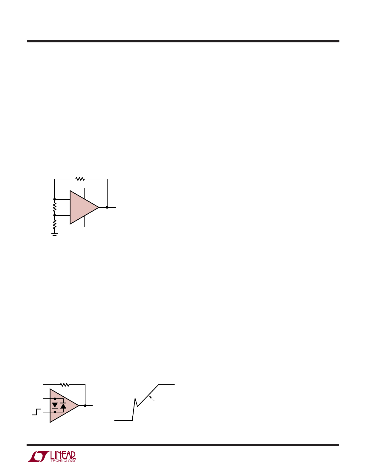
Offset Voltage Adjustment
The input offset voltage of the LT1677 and its drift with
temperature are permanently trimmed at wafer
testing to a low level. However, if further adjustment of
V
is necessary, the use of a 10kΩ nulling potentiometer
OS
will not degrade drift with temperature. Trimming to a
value other than zero creates a drift of (V
e.g., if V
is adjusted to 300µV, the change in drift will be
OS
/300)µV/°C,
OS
1µV/°C (Figure 2).
The adjustment range with a 10kΩ pot is approximately
± 2.5mV. If less adjustment range is needed, the sensitivity and resolution of the nulling can be improved by using
a smaller pot in conjunction with fixed resistors. The
example has an approximate null range of ±200µV
(Figure 3).
10k
1
–
2
INPUT
3
8
LT1677
+
4
–15V
Figure 2. Standard Adjustment
Figure 3. Improved Sensitivity Adjustment
15V
7
6
OUTPUT
1677 F02
12
Input = – 0.5V to 3.5V LT1677 Output
3V
2V
1V
0V
– 0.5V
Figure 1. Voltage Follower with Input Exceeding the Supply Voltage (VS = 3V)
1577 F01a
– 0.5V
3V
2V
1V
0V
1577 F01b
1677fa
WUUU
APPLICATIO S I FOR ATIO
LT1677
Offset Voltage and Drift
Thermocouple effects, caused by temperature gradients
across dissimilar metals at the contacts to the input
terminals, can exceed the inherent drift of the amplifier
unless proper care is exercised. Air currents should be
minimized, package leads should be short, the two input
leads should be close together and maintained at the same
temperature.
The circuit shown to measure offset voltage is also used as
the burn-in configuration for the LT1677, with the supply
voltages increased to ± 20V (Figure 4).
50k*
15V
–
2
100Ω*
3
50k*
Figure 4. Test Circuit for Offset Voltage and
Offset Voltage Drift with Temperature
LT1677
+
7
6
V
1000V
OUT =
4
*RESISTORS MUST HAVE LOW
THERMOELECTRIC POTENTIAL
–15V
V
OUT
OS
1677 F04
Unity-Gain Buffer Application
When R
≤ 100Ω and the input is driven with a fast, large-
F
signal pulse (>1V), the output waveform will look as
shown in the pulsed operation diagram (Figure 5).
During the fast feedthrough-like portion of the output, the
input protection diodes effectively short the output to the
input and a current, limited only by the output short-circuit
protection, will be drawn by the signal generator. With
≥ 500Ω, the output is capable of handling the current
R
F
requirements (IL ≤ 20mA at 10V) and the amplifier stays
in its active mode and a smooth transition will occur.
R
F
–
OUTPUT
+
LT1677
Figure 5. Pulsed Operation
2.5V/µs
1677 F05
As with all operational amplifiers when RF > 2k, a pole will
be created with R
and the amplifier’s input capacitance,
F
creating additional phase shift and reducing the phase
margin. A small capacitor (20pF to 50pF) in parallel with R
F
will eliminate this problem.
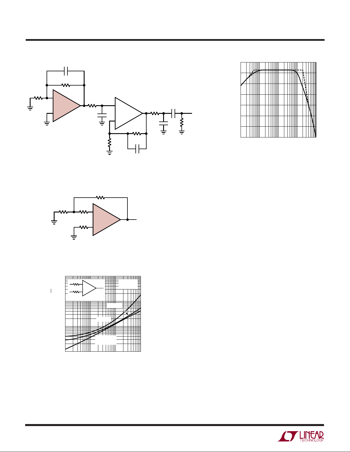
Noise Testing
The 0.1Hz to 10Hz peak-to-peak noise of the LT1677 is
measured in the test circuit shown (Figure 6a). The frequency response of this noise tester (Figure 6b) indicates
that the 0.1Hz corner is defined by only one zero. The test
time to measure 0.1Hz to 10Hz noise should not exceed
ten seconds, as this time limit acts as an additional zero to
eliminate noise contributions from the frequency band
below 0.1Hz.
Measuring the typical 90nV peak-to-peak noise performance of the LT1677 requires special test precautions:
1. The device should be warmed up for at least five
minutes. As the op amp warms up, its offset voltage
changes typically 3µV due to its chip temperature
increasing 10°C to 20°C from the moment the power
supplies are turned on. In the ten-second measurement
interval these temperature-induced effects can easily
exceed tens of nanovolts.
2. For similar reasons, the device must be well shielded
from air currents to eliminate the possibility of
thermoelectric effects in excess of a few nanovolts,
which would invalidate the measurements.
3. Sudden motion in the vicinity of the device can also
“feedthrough” to increase the observed noise.
Current noise is measured in the circuit shown in Figure 7
and calculated by the following formula:
/
12
2
⎡
e
⎢
()
no
⎣
i
=
n
2
nV
−
130
()
M
1 101
()()
•
Ω
101
⎤
⎥
⎦
The LT1677 achieves its low noise, in part, by operating
the input stage at 100µA versus the typical 10µA of most
other op amps. Voltage noise is inversely proportional
while current noise is directly proportional to the square
1677fa
13
LT1677
WUUU
APPLICATIO S I FOR ATIO
0.1µF
100k
100
90
80
10Ω
*DEVICE UNDER TEST
NOTE: ALL CAPACITOR VALUES ARE FOR
NONPOLARIZED CAPACITORS ONLY
–
*
LT1677
+
VOLTAGE GAIN
= 50,000
2k
4.7µF
Figure 6a. 0.1Hz to 10Hz Noise Test Circuit
100Ω
500k
500k
Figure 7
100k
–
+
LT1677
24.3k
+
LT1001
–
100k
0.1µF
1677 F07
70
4.3k
22µF
2.2µF
110k
SCOPE
× 1
= 1M
R
IN
1677 F06a
60
GAIN (dB)
50
40
30
0.01 1 10 100
0.1
FREQUENCY (Hz)
1677 F06b
Figure 6b. 0.1Hz to 10Hz Peak-to-Peak
Noise Tester Frequency Response
root of the input stage current. Therefore, the LT1677’s
current noise will be relatively high. At low frequencies, the
low 1/f current noise corner frequency (≈ 90Hz) minimizes current noise to some extent.
e
no
In most practical applications, however, current noise will
not limit system performance. This is illustrated in the
Total Noise vs Source Resistance plot (Figure 8) where:
Total Noise = [(op amp voltage noise)
+ (current noise RS)2]
1/2
2
+ (resistor noise)
2
1000
100
TOTAL NOISE DENSITY (nV/√Hz)
R
R
SOURCE RESISTANCE = 2R
10
1
0.1
VS = ±15V
T
AT 1kHz
AT 10Hz
RESISTOR
NOISE ONLY
1 10 100
SOURCE RESISTANCE (kΩ)
= 25°C
A
1677 F08
Figure 8. Total Noise vs Source Resistance
Three regions can be identified as a function of source
resistance:
(i) R
≤ 400Ω. Voltage noise dominates
S
(ii) 400Ω ≤ RS ≤ 50k at 1kHz
400Ω ≤ RS ≤ 8k at 10Hz
(iii) RS > 50k at 1kHz
RS > 8k at 10Hz
Current noise
dominates
}
Resistor noise
dominates
}
Clearly the LT1677 should not be used in region (iii), where
total system noise is at least six times higher than the
voltage noise of the op amp, i.e., the low voltage noise
specification is completely wasted. In this region the
LT1792 or LT1793 is the best choice.
1677fa
14

WUUU
APPLICATIO S I FOR ATIO
LT1677
Rail-to-Rail Input
The LT1677 has the lowest voltage noise, offset voltage
and highest gain when compared to any rail-to-rail op
amp. The input common mode range for the LT1677 can
exceed the supplies by at least 100mV. As the common
mode voltage approaches the positive rail (+V
– 0.7V),
S
the tail current for the input pair (Q1, Q2) is reduced,
which prevents the input pair from saturating (refer to the
Simplified Schematic). The voltage drop across the load
resistors R
, RC2 is reduced to less than 200mV, degrad-
C1
ing the slew rate, bandwidth, voltage noise, offset voltage
and input bias current (the cancellation is shut off).
When the input common mode range goes below 1.5V
above the negative rail, the NPN input pair (Q1, Q2) shuts
off and the PNP input pair (Q8, Q9) turns on. The offset
voltage, input bias current, voltage noise and bandwidth
are also degraded. The graph of Offset Voltage Shift vs
Common Mode shows where the knees occur by displaying the change in offset voltage. The change-over points
are temperature dependent, see the graph Common Mode
Range vs Temperature.
Rail-to-Rail Output
The rail-to-rail output swing is achieved by using transistor collectors (Q28, Q29) instead of customary class A-B
emitter followers for the output stage. Referring to the
Simplified Schematic, the output NPN transistor (Q29) sinks
the current necessary to move the output in the negative
direction. The change in Q29’s base emitter voltage is reflected directly to the gain node (collectors of Q20 and Q16).
For large sinking currents, the delta V
of Q29 can domi-
BE
nate the gain. Figure 9 shows the change in input voltage
for a change in output voltage for different load resistors
connected between the supplies. The gain is much higher
for output voltages above ground (Q28 sources current)
since the change in base emitter voltage of Q28 is attenuated by the gain in the PNP portion of the output stage.
Therefore, for positive output swings (output sourcing
current) there is hardly any change in input voltage for any
load resistance. Highest gain and best linearity is achieved
when the output is sourcing current, which is the case in
single supply operation when the load is ground referenced.
Figure 10 shows gains for both sinking and sourcing load
currents for a worst-case load of 600Ω.
RL = 600
RL = 1k
R
= 10k
L
INPUT VOLTAGE (50µV/DIV)
0 5 10 15–5–10–15
TA = 25°C
= ±15V
V
S
CONNECTED TO 0V
R
L
MEASURED ON TEKTRONIX 577 CURVE TRACER
Figure 9. Voltage Gain Split Supply
OUTPUT VOLTAGE (V)
INPUT VOLTAGE (5µV/DIV)
= 25°C
T
A
= 5V
V
S
= 600Ω
R
L
MEASURED ON TEKTRONIX 577 CURVE TRACER
Figure 10. Voltage Gain Single Supply
OUTPUT VOLTAGE (V)
34210
R
L
RL TO 0V
5
TO 5V
1677fa
15

LT1677
U
TYPICAL APPLICATIO S
Microvolt Comparator with Hysteresis
10M5%15k
7
3
+
INPUT
POSITIVE FEEDBACK TO ONE OF THE NULLING TERMINALS
CREATES APPROXIMATELY 5µV OF HYSTERESIS. OUTPUT
CAN SINK 16mA
INPUT OFFSET VOLTAGE IS TYPICALLY CHANGED LESS THAN
5µV DUE TO THE FEEDBACK
2
–
LT1677
1
6
4
1%
15k
1%
3V
OUTPUT
1677 TA03
Precision High Side Current Sense
R11
R10
232Ω
3V Strain Gauge Amplifier
3V
R8
R9
3.4Ω
1k
R*
R*
7.5Ω
R*
R2
R*
5Ω
R3
5.49kR5698Ω
+
–
R2
5Ω
*OMEGA SG-3/350LY11
350Ω, 1%
ALL OTHER RESISTORS 1%
2 • R* + R6
= ≅ 1000
A
V
()
TRIM R11 FOR BRIDGE BALANCE
()
R2 + (R*/2)
R6
R4
5.49k
R4
3V
LT1677
R7
22.1Ω
V
OUT
R*
FOR TEMP
COMPENSATION
R*
OF GAIN
R6
22.1Ω
1677 TA06
SOURCE
LOAD
R
LINE
0.1Ω
< 36V
3V < V
S
R
IN
1k
2
–
7
6
LT1677
3
+
4
ZETEX
BC856B
V
R
OUT
20k
1677 TA07
OUT
V
I
LOAD
OUT
= R
LINE
= 2V/AMP
R
OUT
R
IN
1677fa
16

TYPICAL APPLICATIO S
3V Super Electret Microphone Amplifier with DC Servo
LT1677
U
PANASONIC
ELECTRET
CONDENSER
MICROPHONE
WM-61
(714) 373-7334
2N3906
–1.5V
1.5V
10pF
2
3
C1
–
+
1M
1.5V
LT1677
–1.5V
1.5V
7Hz POLE FOR SERVO
16kHz
R1
ROLL OFF
7
6
4
C4
1µF
R3
1M
–
2
LT1677
3
+
R2
80k
R4
8k
–
2
LT1677
3
+
C3
0.022µF
1.5V
7
6
4
–1.5V
C2
100pF
1.5V
7
6
4
–1.5V
2N3906
R5
2k
20kHz
ROLL OFF
TO
HEADPHONES
1677 TA05
1677fa
17

LT1677
WW
SI PLIFIED SCHE ATIC
S
+V
R34
R32
2k
1.5k
Q28
Q34
Q32
Q35
C1
+
40pF
R1
500Ω
C2
R2
50Ω
+
200µA
Q18
80pF
OUT
R20
R19
R29
10Ω
Q29
C4
20pF
+
C3
+
40pF
Q27
R3
100Ω
Q23
2k
Q20
2k
160µA
Q19
Q31
R54
100Ω
Q26
Q30
100µA
Q22
50µA
R23A
10k
R26
R30
Q14 Q16
Q38
Q25
Q15
R23B
100Ω
2k
10k
R25
R16
R14
R15
S
–V
1677 SS
1k
1k
1k
1k
Q17
R24
R21
R13
S
S
< 0.7V BELOW +V
> 0.7V BELOW +V
CM
CM
0µA V
ID = 100µA V
S
S
< 0.7V BELOW +V
> 0.7V BELOW +V
CM
CM
50µA V
IC = 200µA V
S
S
100Ω
< 1.5V ABOVE –V
> 1.5V ABOVE –V
CM
100Ω
CM
200µA V
100Ω
IA, IB = 0µA V
1677fa
Q11
Q4 Q7
8
PAD
C2B
C2A
R
1k
R
6k
C10
81pF
+
100µA
C1B
C1A
1k
R
PAD
6k
1
R
Q12
Q6
Q10
Q2B
Q3
Q1B Q2A
Q1A
D1
D2
Q5
D4
D3
–IN
+IN
50µA
ID
IC
R9
200Ω
R8
200Ω
Q21
Q13
Q8 Q9
Q24
×2
IB
IA
18

PACKAGE DESCRIPTIO
U
Dimensions in inches (millimeters) unless otherwise noted.
N8 Package
8-Lead PDIP (Narrow 0.300)
(LTC DWG # 05-08-1510)
.400*
(10.160)
MAX
87 6
.255 ± .015*
(6.477 ± 0.381)
5
LT1677
12
.300 – .325
(7.620 – 8.255)
.065
(1.651)
.008 – .015
(0.203 – 0.381)
+.035
.325
–.015
+0.889
8.255
()
–0.381
NOTE:
1. DIMENSIONS ARE
*THESE DIMENSIONS DO NOT INCLUDE MOLD FLASH OR PROTRUSIONS.
MOLD FLASH OR PROTRUSIONS SHALL NOT EXCEED .010 INCH (0.254mm)
INCHES
MILLIMETERS
TYP
.045 – .065
(1.143 – 1.651)
.100
(2.54)
BSC
S8 Package
8-Lead Plastic Small Outline (Narrow 0.150)
(LTC DWG # 05-08-1610)
.045 ±.005
.160
±.005
.228 – .244
(5.791 – 6.197)
.245
MIN
.050 BSC
.189 – .197
(4.801 – 5.004)
8
3
NOTE 3
7
4
(3.302 ± 0.127)
.018 ± .003
(0.457 ± 0.076)
5
6
.130 ± .005
.120
(3.048)
MIN
.150 – .157
(3.810 – 3.988)
NOTE 3
.020
(0.508)
MIN
N8 1002
.030 ±.005
TYP
RECOMMENDED SOLDER PAD LAYOUT
.010 – .020
(0.254 – 0.508)
.008 – .010
(0.203 – 0.254)
NOTE:
1. DIMENSIONS IN
2. DRAWING NOT TO SCALE
3. THESE DIMENSIONS DO NOT INCLUDE MOLD FLASH OR PROTRUSIONS.
MOLD FLASH OR PROTRUSIONS SHALL NOT EXCEED .006" (0.15mm)
Information furnished by Linear Technology Corporation is believed to be accurate and reliable.
However, no responsibility is assumed for its use. Linear Technology Corporation makes no representation that the interconnection of its circuits as described herein will not infringe on existing patent rights.
× 45°
.016 – .050
(0.406 – 1.270)
INCHES
(MILLIMETERS)
(1.346 – 1.752)
0°– 8° TYP
(0.355 – 0.483)
.053 – .069
.014 – .019
TYP
1
2
3
4
.004 – .010
(0.101 – 0.254)
.050
(1.270)
BSC
SO8 0303
1677fa
19

LT1677
TYPICAL APPLICATIO
U
This 2-wire remote Geophone preamp operates on a
current-loop principle and so has good noise immunity.
Quiescent current is ≈10mA for a V
of 2.5V. Excitation
OUT
will cause AC currents about this point of ~± 4mA for a
V
of ~± 1V max. The op amp is configured for a voltage
OUT
2-Wire Remote Geophone Preamp
+
6mA
V
R
R8
–
V
11Ω
3V
C
A
R6
4.99k
R7
24.9k
R1 + R
+
||
R4
≅ 107
L
R
www.geospacecorp.com/default.htm
R2 + R3
AV =
C3
220µF
GEOSPACE
GS-20DX
= 630Ω
R
L
GEOPHONE
(713) 939-7093
R4
14k
R1
365Ω
2
–
–
LT1677
3
+
R3
16.2k
+
LINEAR
TECHNOLOGY
LM334Z
LT1431CZ
gain of ~107. Components R5 and Q1 convert the voltage
into a current for transmission back to R10, which converts it into a voltage again. The LM334 and 2N3904 are
not temperature compensated so the DC output contains
temperature information.
R9
20Ω
Q1
R2
100k
7
4
C2
0.1µF
6
2N3904
R5
243Ω
C4
1000pF
1677 TA04
12V
R10
250Ω
V
OUT
2.5V ±1V
RELATED PARTS
PART NUMBER DESCRIPTION COMMENTS
LT1028/LT1128 Ultralow Noise Precision Op Amps Lowest Noise 0.85nV/√Hz
LT1115 Ultralow Noise, Low distortion Audio Op Amp 0.002% THD, Max Noise 1.2nV/√Hz
LT1124/LT1125 Dual/Quad Low Noise, High Speed Precision Op Amps Similar to LT1007
LT1126/LT1127 Dual/Quad Decompensated Low Noise, High Speed Precision Op Amps Similar to LT1037
LT1226 Low Noise, Very High Speed Op Amp 1GHz, 2.6nV/√Hz, Gain of 25 Stable
LT1498/LT1499 10MHz, 5V/µs, Dual/Quad Rail-to-Rail Input and Output Op Amps Precision C-LoadTM Stable
LT1792 Low Noise, Precision JFET Input Op Amp 4.2nV/√Hz, 10fA/√Hz
LT1793 Low Noise, Picoampere Bias Current Op Amp 6nV/√Hz, 1fA/√Hz, IB = 10pA Max
LT1806 Low Noise, 325MHz Rail-to-Rail Input and Output Op Amp 3.5nV/√Hz
LT1881/LT1882 Dual/Quad Rail-to-Rail Output Picoamp Input Precision Op Amps C
LT1884/LT1885 Dual/Quad Rail-to-Rail Output Picoamp Input Precision Op Amps 2.2MHz Bandwidth, 1.2V/µs SR
C-Load is a trademark of Linear Technology Corporation.
Linear Technology Corporation
20
1630 McCarthy Blvd., Milpitas, CA 95035-7417
(408) 432-1900 ● FAX: (408) 434-0507
●
www.linear-tech.com
to 1000pF, IB = 200pA Max
LOAD
LT 0306 REV A • PRINTED IN USA
© LINEAR TECHNOLOGY CORPORATION 2000
1677fa
 Loading...