

FEATURES
LT1672/LT1673/LT1674
2µA Max, AV ≥ 5 Single, Dual
and Quad Over-The-Top Precision
Rail-to-Rail Input and Output Op Amps
U
DESCRIPTIO
■
Gain of 5 Stable
■
Low Supply Current: 2µA Max per Amplifier
■
Rail-to-Rail Input and Output
■
Low Offset Voltage: 375µV Max
■
Over-The-TopTM Inputs Operate Above V
■
Gain Bandwidth Product: 12kHz
■
Wide Supply Range: 2.2V to 36V
■
Single Supply Input Range: –0.3V to 36V
■
Low Input Bias Current: 250pA
■
Low Input Offset Current: 20pA
■
High A
■
Output Sources and Sinks 500µA Load Current
■
Reverse Battery Protected to 18V
: 100V/mV Minimum Driving 100kΩ Load
VOL
+
U
APPLICATIO S
■
Battery- or Solar-Powered Systems
■
Portable Instrumentation
■
Remote Sensor Amplifier
■
Micropower Filter
■
Photodiode Amplifier
■
High Impedance Circuits
, LTC and LT are registered trademarks of Linear Technology Corporation.
Over-The-Top is a trademark of Linear Technology Corporation.
The LT®1672/LT1673/LT1674 are ultralow power
(IS ≤ 2µA) decompensated (AV ≥ 5) op amps with precision specifications. The extremely low supply current is
combined with excellent amplifier specifications: input
offset voltage is 375µV maximum with a typical drift of
only 0.4µV/°C, input offset current is 100pA maximum. A
minimum open-loop gain (A
) of 100V/mV ensures that
VOL
gain errors are small. The devices’ characteristics change
little over the supply range of 2.2V to ±15V. Supply
rejection is 90dB and the common mode rejection ratio is
90dB. Operation is specified for 3V, 5V and ±15V supplies.
Reverse battery protection (–18V min) and inputs that
operate above the positive supply make the LT1672/
LT1673/LT1674 easy to use in harsh environments.
The low bias currents and offset current of the amplifier
permit the use of megohm level source resistors without
introducing significant errors. Voltage noise at 4µV
P-P
is
remarkably low considering the low supply current. For
unity gain stable versions of these amplifiers, see the
LT1494/LT1495/LT1496.
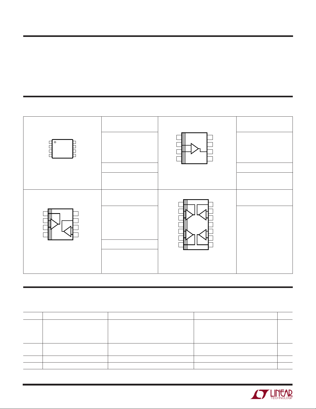
The LT1672 is available in the 8-pin MSOP, PDIP and SO
packages. The LT1673 is available in plastic 8-pin PDIP
and SO-8 packages with the standard dual op amp pinout.
The LT1674 is available in 14-pin PDIP and SO packages.
TYPICAL APPLICATION
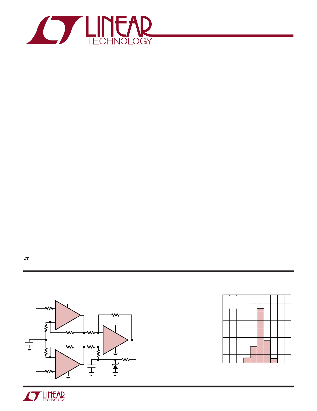
Single Supply, 60µW Precision Instrumentation Amplifier
5V
+
1/2 LT1673
–
1M
–
1/2 LT1673
+
100k1M
100k
1M
0.0047µF
V
V
100k*
IN1
110k
1000pF
110k
100k*
IN2
U
–
LT1672
+
1M
5V
LT1389-2.5
1672/3/4 TA01
1M
V
OUT
= 100
A
V
5V
BANDWIDTH = 1kHz
CMRR = 65dB AT 120Hz
*500V TRANSIENT PROTECTION
TOTAL SUPPLY CURRENT = 12µA
80
70
60
50
40
UNITS
30
20
10
0
–1.5
TC VOS Distribution
120 AMPLIFIERS
= ±2.5V
V
S
–40°C to 85°C
–0.9 –0.3 0.3 1.5
TC VOS (µV/°C)
0.9
1672/3/4 TA02
1
LT1672/LT1673/LT1674
TOP VIEW
S PACKAGE
14-LEAD PLASTIC SO
N PACKAGE
14-LEAD PDIP
1
2
3
4
5
6
7
14
13
12
11
10
9
8
OUT A
–IN A
+IN A
V
+
+IN B
–IN B
OUT B
OUT D
–IN D
+IN D
V
–
+IN C
–IN C
OUT C
A
B
D
C
WWWU
ABSOLUTE AXI U RATI GS
(Note 1)
Total Supply Voltage (V+ to V–) .............................. 36V
Differential Input Voltage ......................................... 36V
Input Current ...................................................... ±10mA
Output Short-Circuit Duration.......................Continuous
Operating Temperature Range (Note 2) .. – 40°C to 85°C
UU
W
PACKAGE/ORDER I FOR ATIO
ORDER PART
NUMBER
NC
1
–IN
2
+IN
3
–
V
4
MS8 PACKAGE
8-LEAD PLASTIC MSOP
T
= 150°C, θJA = 250°C/W
JMAX
OUT A
1
–IN A
2
+IN A
3
–
V
4
TOP VIEW
TOP VIEW
A
8
NC
+
7
V
6
OUT
5
NC
+
V
8
OUT B
7
–IN B
6
B
+IN B
5
LT1672CMS8
LT1672IMS8
MS8 PART MARKING
LTFH
LTFJ
ORDER PART
NUMBER
LT1673CN8
LT1673CS8
LT1673IN8
LT1673IS8
Specified Temperature Range (Note 3)... –40°C to 85°C
Storage Temperature Range ................. –65°C to 150°C
Junction Temperature...........................................150°C
Lead Temperature (Soldering, 10 sec)..................300°C
ORDER PART
TOP VIEW
NC
1
–IN
2
+IN
3
–
V
4
N8 PACKAGE
8-LEAD PDIP
T
= 150°C, θJA = 130°C/ W (N8)
JMAX
= 150°C, θJA = 190°C/ W (S8)
T
JMAX
8
NC
+
V
7
OUT
6
NC
5
S8 PACKAGE
8-LEAD PLASTIC SO
NUMBER
LT1672CN8
LT1672CS8
LT1672IN8
LT1672IS8
S8 PART MARKING
1672
1672I
ORDER PART
NUMBER
LT1674CN
LT1674CS
LT1674IN
LT1674IS
N8 PACKAGE
8-LEAD PDIP
T
= 150°C, θJA = 150°C/ W (N8)
JMAX
T
= 150°C, θJA = 190°C/ W (S8)
JMAX
S8 PACKAGE
8-LEAD PLASTIC SO
S8 PART MARKING
1673
1673I
T
= 150°C, θJA = 110°C/ W (N)
JMAX
T
= 150°C, θJA = 150°C/ W (S)
JMAX
Consult factory for parts specified with wider operating temperature ranges.
ELECTRICAL CHARACTERISTICS
TA = 25°C, VS = 5V, 0V; VS = 3V, 0V; VCM = VO = half supply, unless otherwise noted.
SYMBOL PARAMETER CONDITIONS MIN TYP MAX UNITS
V
OS
I
B
I
OS
2
Input Offset Voltage VS = 5V 150 375 µV
= 3V 200 475 µV
V
S
= 5V, MS8 Package 150 475 µV
V
S
VS = 3V, MS8 Package 200 575 µV
Input Bias Current (Note 5) 250 1000 pA
Input Offset Current (Note 5) 20 100 pA
Input Noise Voltage 0.1Hz to 10Hz 4 µV
VCM = 10V (Note 6) 180 360 nA
P-P
LT1672/LT1673/LT1674
ELECTRICAL CHARACTERISTICS
TA = 25°C, VS = 5V, 0V; VS = 3V, 0V; VCM = VO = half supply, unless otherwise noted.
SYMBOL PARAMETER CONDITIONS MIN TYP MAX UNITS
e
n
i
n
A
VOL
CMRR Common Mode Rejection Ratio VCM = 0V to 4V, VS = 5V 90 106 dB
PSRR Power Supply Rejection Ratio VS = 2.2V to 12V, VCM = VO = 0.5V 90 99 dB
V
OL
V
OH
I
SC
I
S
SR Slew Rate AV = –5, VS = ±10V 1.6 5 V/ms
GBW Gain Bandwidth Product f = 100Hz 12 kHz
Input Noise Voltage Density f = 100Hz 185 nV/√Hz
Input Noise Current Density f = 100Hz 10 fA/√Hz
Large-Signal Voltage Gain VS = 5V, VO = 0.25V to 4.5V, RL = 100k 100 500 V/mV
VS = 3V, VO = 0.25V to 2.5V, RL = 100k 50 250 V/mV
Input Voltage Range 0 36 V
VCM = 0V to 10V, VS = 5V 74 95 dB
Minimum Operating Supply Voltage 2.1 2.2 V
Output Voltage Swing LOW No Load 50 100 mV
I
= 100µA 210 410 mV
SINK
Output Voltage Swing HIGH No Load V+ – 0.07 V+ – 0.035 V
I
= 100µAV
SOURCE
Short-Circuit Current (Note 5) 0.7 1.3 mA
Supply Current per Amplifier (Note 6) 1.5 2 µA
Reverse Supply Voltage IS = 10µA per Amplifier –18 V
+
– 0.32 V+ – 0.160 V
The ● denotes the specifications which apply over the temperature range of 0°C ≤ TA ≤ 70°C. VS = 5V, 0V; VS = 3V, 0V;
VCM = VO = half supply, unless otherwise noted. (Note 3)
SYMBOL PARAMETER CONDITIONS MIN TYP MAX UNITS
V
OS
VOS TC Input Offset Voltage Drift (Note 4) ● 0.4 2 µV/°C
I
B
I
OS
A
VOL
CMRR Common Mode Rejection Ratio VCM = 0.2V to 4V, VS = 5V ● 89 106 dB
PSRR Power Supply Rejection Ratio VS = 2.4V to 12V, VCM = VO = 0.5V ● 89 99 dB
V
OL
V
OH
I
SC
I
S
Input Offset Voltage VS = 5V ● 175 425 µV
= 3V ● 225 525 µV
V
S
V
= 5V, MS8 Package ● 175 525 µV
S
VS = 3V, MS8 Package ● 225 625 µV
Input Bias Current (Note 5) ● 250 1200 pA
VCM = 10V (Note 6) ● 240 500 nA
Input Offset Current (Note 5) ● 20 120 pA
Large-Signal Voltage Gain VS = 5V, VO = 0.25V to 4.5V, RL = 100k ● 75 280 V/mV
VS = 3V, VO = 0.25V to 2.5V, RL = 100k ● 40 150 V/mV
Input Voltage Range ● 0.2 36 V
VCM = 0.2V to 10V, VS = 5V ● 64 85 dB
Minimum Operating Supply Voltage ● 2.3 2.4 V
Output Voltage Swing LOW No Load ● 55 110 mV
I
= 100µA ● 225 450 mV
SINK
Output Voltage Swing HIGH No Load ● V+ – 0.08 V+ – 0.04 V
I
= 100µA ● V+ – 0.36 V+ – 0.18 V
SOURCE
Short-Circuit Current (Note 5) ● 0.6 1.1 mA
Supply Current per Amplifier (Note 6) ● 1.9 2.8 µA
3
LT1672/LT1673/LT1674
ELECTRICAL CHARACTERISTICS
The ● denotes the specifications which apply over the temperature range of –40°C ≤ TA ≤ 85°C. VS = 5V, 0V; VS = 3V, 0V;
VCM = VO = half supply, unless otherwise noted. (Note 3)
SYMBOL PARAMETER CONDITIONS MIN TYP MAX UNITS
V
OS
VOS TC Input Offset Voltage Drift (Note 4) ● 0.4 2 µV/°C
I
B
I
OS
A
VOL
CMRR Common Mode Rejection Ratio VCM = 0.2V to 4V, VS = 5V ● 88 106 dB
PSRR Power Supply Rejection Ratio VS = 2.7V to 12V, VCM = VO = 0.5V ● 88 99 dB
V
OL
V
OH
I
SC
I
S
Input Offset Voltage VS = 5V ● 200 475 µV
= 3V ● 250 575 µV
V
S
V
= 5V, MS8 Package ● 200 575 µV
S
VS = 3V, MS8 Package ● 250 675 µV
Input Bias Current (Note 5) ● 250 1700 pA
VCM = 10V (Note 6) ● 275 750 nA
Input Offset Current (Note 5) ● 20 170 pA
Large-Signal Voltage Gain VS = 5V, VO = 0.25V to 4.5V, RL = 100k ● 55 215 V/mV
VS = 3V, VO = 0.25V to 2.5V, RL = 100k ● 30 115 V/mV
Input Voltage Range ● 0.2 36 V
VCM = 0.2V to 10V, VS = 5V ● 62 75 dB
Minimum Operating Supply Voltage ● 2.6 2.7 V
Output Voltage Swing LOW No Load ● 60 120 mV
I
= 100µA ● 245 490 mV
SINK
Output Voltage Swing HIGH No Load ● V+ – 0.10 V+ – 0.05 mV
I
= 100µA ● V+ – 0.38 V+ – 0.19 mV
SOURCE
Short-Circuit Current (Note 5) ● 0.4 0.9 mA
Supply Current per Amplifier (Note 6) ● 2.1 3.1 µA
TA = 25°C, VS = ±15V, VCM = VO = 0V, unless otherwise noted.
SYMBOL PARAMETER CONDITIONS MIN TYP MAX UNITS
V
OS
I
B
I
OS
A
VOL
CMRR Common Mode Rejection Ratio VCM = –15V to 14V 100 120 dB
PSRR Power Supply Rejection Ratio VS = ±5V to ±15V 96 120 dB
V
OL
V
OH
I
SC
I
S
Input Offset Voltage 200 575 µV
MS8 Package 200 675 µV
Input Bias Current 25 1000 pA
Input Offset Current 20 100 pA
Large-Signal Voltage Gain VO = ±10V, RL = 100k 100 360 V/mV
Input Voltage Range –15 21 V
Output Voltage Swing LOW RL = 1M –14.85 –14.70 V
RL = 100k –14.75 –14.50 V
Output Voltage Swing HIGH RL = 1M 14.78 14.89 V
RL = 100k 14.62 14.81 V
Short-Circuit Current 0.7 1.5 mA
Supply Current per Amplifier 1.9 2.8 µA
4

LT1672/LT1673/LT1674
ELECTRICAL CHARACTERISTICS
The ● denotes the specifications which apply over the temperature range of 0°C ≤ TA ≤ 70°C, VS = ±15V, VCM = VO = 0V,
unless otherwise noted. (Note 3)
SYMBOL PARAMETER CONDITIONS MIN TYP MAX UNITS
V
OS
I
B
I
OS
A
VOL
CMRR Common Mode Rejection Ratio VCM = –14.8V to 14V ● 98 120 dB
PSRR Power Supply Rejection Ratio VS = ±5V to ±15V ● 94 120 dB
V
OL
V
OH
I
SC
I
S
The ● denotes the specifications which apply over the temperature range of –40°C ≤ TA ≤ 85°C, VS = ±15V, VCM = VO = 0V,
unless otherwise noted. (Note 3)
SYMBOL PARAMETER CONDITIONS MIN TYP MAX UNITS
V
OS
I
B
I
OS
A
VOL
CMRR Common Mode Rejection Ratio VCM = –14.8V to 14V ● 96 114 dB
PSRR Power Supply Rejection Ratio VS = ±5V to ±15V ● 92 120 dB
V
OL
V
OH
I
SC
I
S
Note 1: Absolute Maximum Ratings are those values beyond which the life
of the device may be impaired.
Note 2: The LT1672C/LT1673C/LT1674C and LT1672I/LT1673I/LT1674I
are guaranteed functional over the Operating Temperature Range of –40°C
to 85°C.
Note 3: The LT1672C/LT1673C/LT1674C are guaranteed to meet specified
performance from 0°C to 70°C. The LT1672C/LT1673C/LT1674C are
designed, characterized and expected to meet specified performance from
Input Offset Voltage ● 225 625 µV
MS8 Package ● 225 725 µV
Input Bias Current ● 250 1200 pA
Input Offset Current ● 20 120 pA
Large-Signal Voltage Gain VO = ±10V, RL = 100k ● 60 240 V/mV
Input Voltage Range ● –14.8 21 V
Output Voltage Swing LOW RL = 1M ● –14.84 –14.67 V
RL = 100k ● –14.73 –14.46 V
Output Voltage Swing HIGH RL = 1M ● 14.76 14.88 V
RL = 100k ● 14.58 14.79 mV
Short-Circuit Current ● 0.6 1.3 mA
Supply Current per Amplifier ● 2.4 3.5 µA
Input Offset Voltage ● 250 675 µV
MS8 Package ● 250 775 µV
Input Bias Current ● 250 1700 pA
Input Offset Current ● 20 170 pA
Large-Signal Voltage Gain VO = ±10V, RL = 100k ● 50 200 V/mV
Input Voltage Range ● –14.8 21 V
Output Voltage Swing LOW RL = 1M ● –14.83 –14.66 V
RL = 100k ● –14.72 –14.44 V
Output Voltage Swing HIGH RL = 1M ● 14.74 14.87 V
RL = 100k ● 14.54 14.77 V
Short-Circuit Current ● 0.4 1.1 mA
Supply Current per Amplifier ● 2.8 4.2 µA
–40°C to 85°C but are not tested or QA sampled at these temperatures.
The LT1672I/LT1673I/LT1674I are guaranteed to meet specified
performance from –40°C to 85°C.
Note 4: This parameter is not 100% tested.
Note 5: V
tests.
Note 6: V
tests.
= 5V limit guaranteed by correlation to VS = 3V and VS = ±15V
S
= 3V limit guaranteed by correlation to VS = 5V and VS = ±15V
S
5

LT1672/LT1673/LT1674
W
U
TYPICAL PERFORMANCE CHARACTERISTICS
Distribution of Input
Offset Voltage
20
18
16
14
12
10
8
6
PERCENT OF UNITS (%)
4
2
0
–400
–300 –100
–200
INPUT OFFSET VOLTAGE (µV)
0
Output Saturation Voltage
vs Load Current (Output Low)
1000
VS = 5V, 0V
= 85°C
T
A
100
TA = –40°C
SATURATION VOLTAGE (mV)
VS = 5V, 0V
LT1672/73/74
5600 AMPLIFIERS
300
200
100
1672/73/74 G01
TA = 25°C
400
Supply Current vs Temperature
3.0
2.5
2.0
1.5
1.0
0.5
SUPPLY CURRENT PER AMPLIFIER (µA)
0
–40
–20 0
VS = ±15V
40 80 100
20 60
TEMPERATURE (°C)
Output Saturation Voltage
vs Load Current (Output High)
1000
VS = 5V, 0V
100
SATURATION VOLTAGE (mV)
T
A
= 85°C
TA = –40°C
VS = ±2.5V
TA = 25°C
1672/3/4 G02
Minimum Supply Voltage
200
150
100
TA = 85°C
50
0
CHANGE IN OFFSET VOLTAGE (µV)
–50
1
TOTAL SUPPLY VOLTAGE (V)
TA = 25°C
T
2
Input Bias Current
vs Common Mode Voltage
300
VS = 5V, 0V
200
100
1.5
INPUT BIAS CURRENT (nA)
0.5
TA = –40°C
= –40°C
A
3
TA = 85°C
4
TA = 85°C
TA = 25°C
TA = –40°C
TA = 25°C
5
1672/3/4 G03
10
0.1
LOAD CURRENT (µA)
Gain and Phase Shift
vs Frequency
90
80
70
60
50
40
30
VOLTAGE GAIN (dB)
20
10
0
–10
100
GAIN
101 1000100
1k 10k
FREQUENCY (Hz)
1672/3/4 G04
VS = ±2.5V
PHASE
1672/3/4 G07
120
100
80
PHASE SHIFT (DEG)
60
40
20
0
–20
–40
–60
–80
10
0.1
LOAD CURRENT (µA)
Noise Voltage Spectrum
300
VS = ±2.5V
250
200
150
100
NOISE VOLTAGE (nV/√Hz)
50
0
1
FREQUENCY (Hz)
101 1000100
1672/3/4 G05
10 100
1672/3/4 G08
–0.5
2
3
1–1 9
0
COMMON MODE VOLTAGE (V)
Noise Current Spectrum
100
VS = ±2.5V
80
60
40
CURRENT NOISE (fA/√Hz)
20
0
1
FREQUENCY (Hz)
6
7
4
5
10 100
8
1672/3/4 G06
1672/3/4 G09
10
6

W
1672/3/4 G15
FREQUENCY (Hz)
10
0.1
OUTPUT IMPEDANCE (kΩ)
1
10
100
100 1k 10k
AV = 10
AV = 5
VS = ±2.5V
U
TYPICAL PERFORMANCE CHARACTERISTICS
LT1672/LT1673/LT1674
Gain Bandwidth and Phase
Margin vs Supply Voltage Capacitive Load Handling
25 30
1672/3/4 G10
80
70
PHASE MARGIN (DEG)
60
50
40
30
16
MEASURED AT
= 5
A
V
14
12
10
FREQUENCY (kHz)
8
6
0
5
PHASE MARGIN
GBW
10 15 20
SUPPLY VOLTAGE (V)
Common Mode Rejection Ratio
vs Frequency
100
90
80
70
60
50
40
30
20
COMMON MODE REJECTIO RATIO (dB)
10
0
100
1k 10k 20k
FREQUENCY (Hz)
VS = ±2.5V
1672/3/4 G13
0.1Hz to 10Hz
Output Voltage Noise
VS = ±15V
V
= 0V
CM
OUTPUT VOLTAGE (2µV/DIV)
TIME (1s/DIV)
Power Supply Rejection Ratio
vs Frequency
100
90
80
70
60
50
40
30
20
10
POWER SUPPLY REJECTION RATIO (dB)
0
10
+PSRR
–PSRR
100 1k 10k
FREQUENCY (Hz)
1672/3/4 G07
VS = ±2.5V
1672/3/4 G14
80
VS = ±2.5V
70
60
50
40
30
OVERSHOOT (%)
20
10
0
10
AV = 5
100 1k 10k
CAPACITIVE LOAD (pF)
Output Impedance vs Frequency
AV = 10
1672/3/4 G12
Open-Loop Gain
Warm-Up Drift vs Time
40
30
20
10
–10
–20
OFFSET VOLTAGE CHANGE (µV)
–30
– 40
VS = ±15V
0
V
= ±2.5V
S
40 80 120 20014020 60 100 180
0
TIME AFTER POWER-UP (SEC)
160
1672/3/4 G16
VS = 5V, 0V
20
15
10
5
0
–5
–10
OFFSET VOLTAGE CHANGE (µV)
–15
–20
0
R
= 1M
L
R
= 100k
L
12 4
3
OUTPUT VOLTAGE (V)
VS = 5V, 0V
5
1672/3/4 G17
6
Open-Loop Gain
VS = ±15V
80
60
40
20
0
–20
–40
OFFSET VOLTAGE CHANGE (µV)
–60
–80
–20 –15
RL = 100k
RL = 1M
–10 –5 0 5 1510
OUTPUT VOLTAGE (V)
VS = ±15V
20
1672/3/4 G18
7

LT1672/LT1673/LT1674
W
U
TYPICAL PERFORMANCE CHARACTERISTICS
Small-Signal Response Small-Signal Response Large-Signal Response
VS = ±15V
= 100pF
C
L
= 5
A
V
1672/3/4 G19 1672/3/4 G20 1672/3/4 G21
= 5V
V
S
= 100pF
C
L
= 5
A
V
WUUU
APPLICATIO S I FOR ATIO
Start-Up Characteristics
Micropower op amps are sometimes not micropower
during start-up, wreaking havoc on low current supplies.
In the worst case, there may not be enough supply current
available to take the system up to nominal voltages. Figure
1 is a graph of LT1673 supply current vs supply voltage
for the three limit cases of input offset that could occur
during start-up. The circuits are shown in Figure 2. One
circuit creates a positive offset, forcing the output to come
up saturated high. Another circuit creates a negative
offset, forcing the output to come up saturated low, while
the last brings up the output at half supply. In all cases, the
supply current is well behaved. Supply current is highest
with the output forced high, so if one amplifier is unused,
it is best to force the output low or at half supply.
5
4
3
2
OUTPUT HIGH
OUTPUT LOW
= 5V
V
S
C
= 100pF
L
= 5
A
V
+
V
+
–
–
V
OUTPUT HIGH
+
V
+
–
–
V
OUTPUT LOW
200k
+
V
+
–
820k
–
V
OUTPUT AT VS/2
16/2/3/4 F02
Figure 2. Circuits for Start-Up Characteristics
Reverse Battery
The LT1672/LT1673/LT1674 are protected against reverse
battery voltages up to 18V. In the event a reverse battery
condition occurs, the supply current is typically less than
100nA (inputs grounded and outputs open). For typical
single supply applications with ground referred loads and
feedback networks, no other precautions are required. If
the reverse battery condition results in a negative voltage
at either the input pins or output pin, the current into the
pin should be limited by an external resistor to less than
10mA.
8
1
SUPPLY CURRENT PER AMPLIFIER (µA)
0
1
0
TOTAL SUPPLY VOLTAGE (V)
2
OUTPUT VS/2
3
Figure 1. Start-Up Characteristics
4
1672/3/4 FO1
Inputs
While the LT1672/LT1673/LT1674 will function normally
5
with its inputs taken above the positive supply, the common mode range does not extend beyond approximately
300mV below the negative supply at room temperature.

WUUU
APPLICATIO S I FOR ATIO
LT1672/LT1673/LT1674
The device will not be damaged if the inputs are taken lower
than 300mV below the negative supply as long as the current out of the pin is limited to less than 10mA. However,
the output phase is not guaranteed and the supply current
will increase.
Output
The graph, Capacitive Load Handling, shows amplifier stability with the output biased at half supply. If the output is
to be operated within about 100mV of the positive rail, the
allowable load capacitance is less. With this output voltage, the worst case occurs at AV = 5 and light loads, where
the load capacitance should be less than 500pF with a 5V
supply and less than 100pF with a 30V supply.
Rail-to-Rail Operation
The simplified schematic, Figure 3, details the circuit
design approach of the
LT1672/LT1673/LT1674
. The
amplifier topology is a three-stage design consisting of a
rail-to-rail input stage, that continues to operate with the
inputs above the positive rail, a folded cascode second
stage that develops most of the voltage gain, and a rail-torail common emitter stage that provides the current gain.
The input stage is formed by two diff amps Q1-Q2 and Q3Q6. For signals with a common mode voltage between V
EE
and (VCC – 0.8V), Q1 and Q2 are active. When the input
common mode exceeds (VCC – 0.8V), Q7 turns on,
diverting the current from diff amp Q1-Q2 to current
mirror Q8-Q9. The current from Q8 biases on the other
diff amp consisting of PNP’s Q5-Q6 and NPN’s Q3-Q4.
Though Q5-Q6 are driven from the emitters rather than
the base, the basic diff amp action is the same. When the
common mode voltage is between (VCC – 0.8V) and VCC,
devices Q3 and Q4 act as followers, forming a buffer
between the amplifier inputs and the emitters of the Q5Q6. If the common mode voltage is taken above VCC,
Schottky diodes D1 and D2 reverse bias and devices Q3
and Q4 then act as diodes. The diff amp formed by Q5-Q6
operates normally, however, the input bias current increases to the emitter current of Q5-Q6, which is typically
180nA. The graph, Input Bias Current vs Common Mode
Voltage found in the Typical Performance Characteristics
section, shows these transitions at three temperatures.
The collector currents of the two-input pairs are combined
in the second stage consisting of Q11 to Q16, which
furnishes most of the voltage gain. Capacitor C1 sets the
amplifier bandwidth. The output stage is configured for
maximum swing by the use of common emitter output
devices Q21 and Q22. Diodes D4 to D6 and current source
Q15 set the output quiescent current.
Q10 Q13
+
IN
–
IN
Q2
Q1
D1 D2 D3
Q4 Q16 Q17(V+) – 0.8V Q19
Q3
Q5
Q9
Q7
Q6
Q8
Figure 3. Simplified Schematic
Q14 Q15
Q11
Q12
R1 R2 I
C1
2
D7
+
I
1
D4
D5
D6
Q20
Q18
Q21
OUT
Q22
1672/3/4 F03
9

LT1672/LT1673/LT1674
U
TYPICAL APPLICATIO S
Battery Current Monitor
I
A2
1/2 LT1673
L
CHARGE
DISCHARGE
–
+
2N3904
R
B
R
R
A
A
DISCHARGE
OUT
R
0.1Ω
SENSE
CHARGE
OUT
R
A
R
A
2N3904
PACKAGE DESCRIPTIO
0.007
(0.18)
0.021
± 0.006
(0.53 ± 0.015)
* DIMENSION DOES NOT INCLUDE MOLD FLASH, PROTRUSIONS OR GATE BURRS. MOLD FLASH,
PROTRUSIONS OR GATE BURRS SHALL NOT EXCEED 0.006" (0.152mm) PER SIDE
** DIMENSION DOES NOT INCLUDE INTERLEAD FLASH OR PROTRUSIONS.
INTERLEAD FLASH OR PROTRUSIONS SHALL NOT EXCEED 0.006" (0.152mm) PER SIDE
° – 6° TYP
0
SEATING
Over-the-Top Comparator with Hysteresis
5V
–
A1
1/2 LT1673
12V
IN1
(0V TO 12V)
+
IN2
R
B
V
= I
O
L RSENSE
()
R
A
FOR RA = 10k, RB = 100k (RB/RA ≥5)
R
B
V
O
= 1V/A
I
L
1672/3/4 TA04
(0V TO 12V)
HYSTERESIS =
IS < 10µA
U
Dimensions in inches (millimeters) unless otherwise noted.
MS8 Package
8-Lead Plastic MSOP
(LTC DWG # 05-08-1660)
PLANE
0.043
(1.10)
MAX
0.009 – 0.015
(0.22 – 0.38)
0.0256
(0.65)
BSC
0.034
(0.86)
REF
0.005
(0.13 ± 0.05)
± 0.002
0.118 ± 0.004*
(3.00 ± 0.102)
0.193 ± 0.006
(4.90 ± 0.15)
10k
10k
+
–
V
CC
100
8
12
5V (V
LT1672
1M
7
1M
)
CC
2N5087
2N5210
6
5
0.118 ± 0.004**
4
3
1M
1672/3/4 TA03
(3.00 ± 0.102)
MSOP (MS8) 1100
1M
V
OUT
0.300 – 0.325
(7.620 – 8.255)
0.065
(1.651)
0.009 – 0.015
(0.229 – 0.381)
+0.035
0.325
–0.015
+0.889
8.255
()
–0.381
*THESE DIMENSIONS DO NOT INCLUDE MOLD FLASH OR PROTRUSIONS.
MOLD FLASH OR PROTRUSIONS SHALL NOT EXCEED 0.010 INCH (0.254mm)
TYP
0.045 – 0.065
(1.143 – 1.651)
0.100
(2.54)
BSC
10
N8 Package
8-Lead PDIP (Narrow 0.300)
(LTC DWG # 05-08-1510)
0.130 ± 0.005
(3.302 ± 0.127)
0.125
(3.175)
MIN
0.018 ± 0.003
(0.457 ± 0.076)
0.020
(0.508)
MIN
0.255 ± 0.015*
(6.477 ± 0.381)
0.400*
(10.160)
MAX
876
12
3
5
4
N8 1098

PACKAGE DESCRIPTIO
LT1672/LT1673/LT1674
U
Dimensions in inches (millimeters) unless otherwise noted.
S8 Package
8-Lead Plastic Small Outline (Narrow 0.150)
(LTC DWG # 05-08-1610)
0.189 – 0.197*
(4.801 – 5.004)
7
8
5
6
0.228 – 0.244
(5.791 – 6.197)
0.010 – 0.020
(0.254 – 0.508)
0.008 – 0.010
(0.203 – 0.254)
*
DIMENSION DOES NOT INCLUDE MOLD FLASH. MOLD FLASH
SHALL NOT EXCEED 0.006" (0.152mm) PER SIDE
**
DIMENSION DOES NOT INCLUDE INTERLEAD FLASH. INTERLEAD
FLASH SHALL NOT EXCEED 0.010" (0.254mm) PER SIDE
× 45°
0°– 8° TYP
0.016 – 0.050
(0.406 – 1.270)
S Package
14-Lead Plastic Small Outline (Narrow 0.150)
(LTC DWG # 05-08-1610)
0.053 – 0.069
(1.346 – 1.752)
0.014 – 0.019
(0.355 – 0.483)
TYP
13
14
1
0.337 – 0.344*
(8.560 – 8.738)
12
0.150 – 0.157**
(3.810 – 3.988)
3
2
4
0.004 – 0.010
(0.101 – 0.254)
0.050
(1.270)
BSC
SO8 1298
11
10
8
9
0.228 – 0.244
(5.791 – 6.197)
0.010 – 0.020
(0.254 – 0.508)
0.008 – 0.010
(0.203 – 0.254)
*
DIMENSION DOES NOT INCLUDE MOLD FLASH. MOLD FLASH
SHALL NOT EXCEED 0.006" (0.152mm) PER SIDE
**
DIMENSION DOES NOT INCLUDE INTERLEAD FLASH. INTERLEAD
FLASH SHALL NOT EXCEED 0.010" (0.254mm) PER SIDE
× 45°
0° – 8° TYP
0.016 – 0.050
(0.406 – 1.270)
Information furnished by Linear Technology Corporation is believed to be accurate and reliable.
However, no responsibility is assumed for its use. Linear Technology Corporation makes no representation that the interconnection of its circuits as described herein will not infringe on existing patent rights.
0.053 – 0.069
(1.346 – 1.752)
0.014 – 0.019
(0.355 – 0.483)
TYP
0.150 – 0.157**
(3.810 – 3.988)
1
3
2
4
0.050
(1.270)
BSC
5
7
6
0.004 – 0.010
(0.101 – 0.254)
S14 1298
11

LT1672/LT1673/LT1674
U
TYPICAL APPLICATIO
Micropower Photodiode Amplifier
C1
20pF
I
PHOTODIODE
R1
10M
V
GAIN: AZ = 10MΩ =
+
S
10% TO 90% RISE TIME: t
BANDWIDTH: BW = 1.7kHz
V
OUT
I
PHOTODIODE
= 260µs
r
–
880nm IR
PHOTODIODE
λ
OPTO-DIODE CORP
ODD-45W
C
D
170pF
+
LT1672
V
S
–
V
OUT
VS = ±1.2V TO ±15V
C1, CD SATISFY GAIN OF 5
STABILITY REQUIREMENT AT AC.
1672/3/4 TA05
RELATED PARTS
PART NUMBER DESCRIPTION COMMENTS
LTC®1440/41/42 Micropower Single/Dual Comparators with 1% Reference LTC1440: Single, LTC1441/42: Dual
LTC1443/LTC1444/LTC1445 Micropower Quad Comparators with 1% Reference LTC1443: 1.182 Reference
LTC1444/45: 1.221V Reference and Adjustable Hysteresis
LT1466/LT1467 75µA Dual/Quad Rail-to-Rail Input and Output Op Amps 390µV V
LT1490A/LT1491A 50µA Dual/Quad Rail-to-Rail Input and Output Op Amps 950µV V
LT1494/LT1495/LT1496 1.5µA Max Single/Dual/Quad Over-the-Top Unity Gain Stable Version of the LT1672/LT1673/LT1674
Precision Rail-to-Rail Input and Output Op Amps
LTC1540 Nanopower Single Comparator with 1% Reference 350nA Supply Current
LT1636 Single Over-the-Top Micropower, Rail-to-Rail 225µV V
Input and Output Op Amp Shutdown Pin, MSOP
LT2078/LT2079 55µA Dual/Quad Single Supply Op Amps 120µV V
LT2178/LT2179 17µA Dual/Quad Single Supply Op Amps 120µV V
LT1782 Micropower, Over-The-Top, SOT-23, Rail-to-Rail SOT-23, 800µV V
Input and Output Op Amp Gain-Bandwidth = 200kHz, Shutdown Pin
LT1783 1.2MHz, Over-The-Top, Micropower, Rail-to-Rail SOT-23, 800µV V
Input and Output Op Amp in SOT-23 Gain-Bandwidth = 1.2MHz, Shutdown Pin
, Gain Bandwidth = 120kHz
OS(MAX)
, Gain Bandwidth = 200kHz
OS(MAX)
, IS = 55µA (Max), Gain Bandwidth = 200kHz,
OS(MAX)
, Gain Bandwidth = 200kHz
OS(MAX)
, Gain Bandwidth = 60kHz
OS(MAX)
, IS = 55µA (Max),
OS(MAX)
, IS = 300µA (Max),
OS(MAX)
12
Linear Technology Corporation
1630 McCarthy Blvd., Milpitas, CA 95035-7417
(408) 432-1900 ● FAX: (408) 434-0507
●
www.linear-tech.com
167234f LT/TP 0101 4K • PRINTED IN USA
LINEAR TECHNOLOGY CORPORATION 2001
 Loading...