


FEATURES
■
Allows Safe Board Insertion and Removal
from a Live – 48V Backplane
■
Operates from –10V to –80V
■
Programmable Inrush Current
■
Programmable Electronic Circuit Breaker
■
Programmable Overvoltage Protection
■
Programmable Undervoltage Lockout
■
Power Good Control Output
U
APPLICATIO S
■
Central Office Switching
■
–48V Distributed Power Systems
■
Negative Power Supply Control
LT1640L/LT1640H
Negative Voltage
Hot Swap Controller
U
DESCRIPTIO
The LT®1640L/LT1640H is an 8-pin, negative voltage Hot
SwapTM controller that allows a board to be safely inserted
and removed from a live backplane. Inrush current is
limited to a programmable value by controlling the gate
voltage of an external N-channel pass transistor. The pass
transistor is turned off if the input voltage is less than the
programmable undervoltage threshold or greater than the
overvoltage threshold. A programmable electronic circuit
breaker protects the system against shorts. The PWRGD
(LT1640L) or PWRGD (LT1640H) signal can be used to
directly enable a power module. The LT1640L is designed
for modules with a low enable input and the LT1640H for
modules with a high enable input.
The LT1640L/LT1640H is available in 8-pin PDIP and SO
packages.
, LTC and LT are registered trademarks of Linear Technology Corporation.
Hot Swap is a trademark of Linear Technology Corporation.
TYPICAL APPLICATIO
(SHORT PIN)
GND
UV = 37V
OV = 71V
–48V
* DIODES INC. SMAT70A
†
THESE COMPONENTS ARE APPLICATION
SPECIFIC AND MUST BE SELECTED BASED
UPON OPERATING CONDITIONS AND DESIRED
PERFORMANCE. SEE APPLICATIONS
INFORMATION.
GND
†
R4
562k
1%
3
UV
†
R5
9.09k
2
1%
OV
†
R6
V
SENSE
10k
1%
*
EE
4
56
†
R1
0.02Ω
43
5%
21
8
V
DD
LT1640L
GATE DRAIN
†
C1
150nF
25V
IRF530
C3
0.1µF
100V
U
Input Inrush Current
INRUSH
1
PWRGD
7
1N4148
†
R2
R3
†
C4
100µF
100V
18k
5%
C2
3.3nF
100V
1
4
ON/OFF
+
V
IN
–
V
IN
LUCENT
JW050A1-E
2
V
SENSE
TRIM
SENSE
V
OUT
OUT
9
+
8
+
–
–
C5
+
7
100µF
6
16V
5
1640 TA01
10Ω
5%
Q1
+
CURRENT
1A/DIV
GATE – V
EE
10V/DIV
DRAIN
50V/DIV
V
EE
50V/DIV
5V
CONTACT
BOUNCE
5ms/DIV
1640 F06b
1640lhfb
1
LT1640L/LT1640H
WW
W
ABSOLUTE MAXIMUM RATINGS
U
(Note 1), All Voltages Referred to V
Supply Voltage (VDD – VEE) .................... –0.3V to 100V
DRAIN, PWRGD, PWRGD Pins ............... –0.3V to 100V
SENSE, GATE Pins.................................... –0.3V to 20V
UV, OV Pins .............................................. –0.3V to 60V
Maximum Junction Temperature ......................... 125°C
WU
/
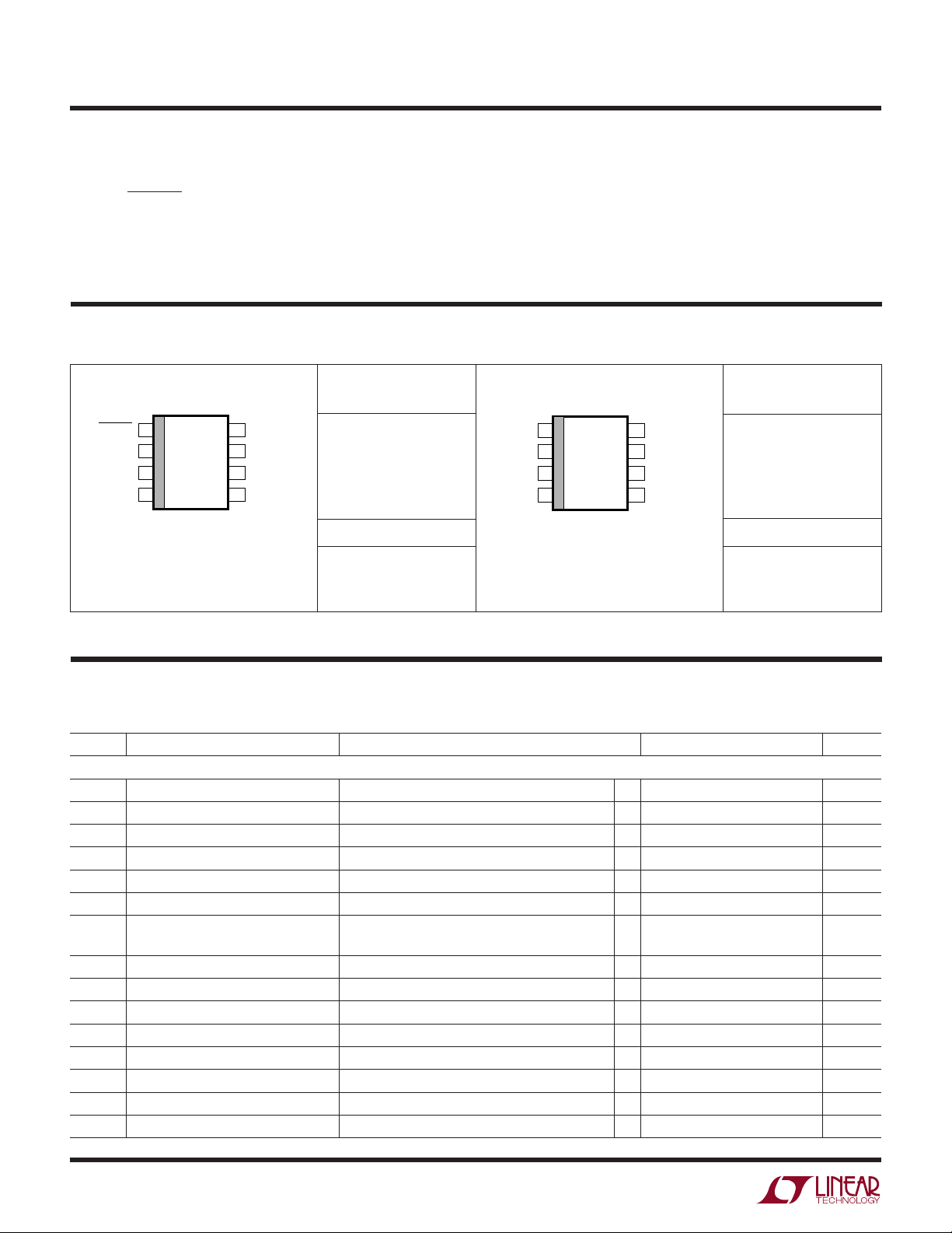
PACKAGE
PWRGD
1
OV
2
UV
3
V
4
EE
N8 PACKAGE
8-LEAD PDIP
T
= 125°C, θJA = 120°C/W (N8)
JMAX
T
= 125°C, θJA = 150°C/W (S8)
JMAX
O
RDER I FOR ATIO
TOP VIEW
V
8
DD
DRAIN
7
GATE
6
SENSE
5
S8 PACKAGE
8-LEAD PLASTIC SO
S8 PART MARKING
ORDER PART
NUMBER
LT1640LCN8
LT1640LCS8
LT1640LIN8
LT1640LIS8
1640L
1640LI
EE
Operating Temperature Range
LT1640LC/LT1640HC ............................. 0°C to 70°C
LT1640LI/LT1640HI .......................... – 40°C to 85°C
Storage Temperature Range ................ –65°C to 150°C
Lead Temperature (Soldering, 10 sec)................. 300°C
U
ORDER PART
NUMBER
LT1640HCN8
LT1640HCS8
LT1640HIN8
LT1640HIS8
S8 PART MARKING
1640H
1640HI
PWRGD
OV
UV
V
EE
N8 PACKAGE
8-LEAD PDIP
T
JMAX
T
JMAX
TOP VIEW
1
2
3
4
= 125°C, θJA = 120°C/W (N8)
= 125°C, θJA = 150°C/W (S8)
8
7
6
5
S8 PACKAGE
8-LEAD PLASTIC SO
V
DD
DRAIN
GATE
SENSE
Consult LTC Marketing for parts specified with wider operating temperature ranges.
ELECTRICAL CHARACTERISTICS
temperature range, otherwise specifications are at T
SYMBOL PARAMETER CONDITIONS MIN TYP MAX UNITS
DC
V
DD
I
DD
V
CB
I
PU
I
PD
I
SENSE
∆V
V
UVH
V
UVL
V
UVHY
I
INUV
V
OVH
V
OVL
V
OVHY
I
INOV
GATE
Supply Operating Range ● 10 80 V
Supply Current UV = 3V, OV = VEE, SENSE = V
Circuit Breaker Trip Voltage VCB = (V
GATE Pin Pull-Up Current Gate Drive On, V
GATE Pin Pull-Down Current Any Fault Condition 24 50 70 mA
SENSE Pin Current V
External Gate Drive (V
UV Pin High Threshold Voltage UV Low to High Transition ● 1.213 1.243 1.272 V
UV Pin Low Threshold Voltage UV High to Low Transition ● 1.198 1.223 1.247 V
UV Pin Hysteresis 20 mV
UV Pin Input Current VUV = V
OV Pin High Threshold Voltage OV Low to High Transition ● 1.198 1.223 1.247 V
OV Pin Low Threshold Voltage OV High to Low Transition ● 1.165 1.203 1.232 V
OV Pin Hysteresis 20 mV
OV Pin Input Current VOV = V
SENSE
(V
GATE
GATE
The ● denotes the specifications which apply over the full operating
= 25°C. (Note 2), V
A
– VEE) ● 40 50 60 mV
SENSE
= V
GATE
= 50mV –20 µA
– VEE), 15V ≤ VDD ≤ 80V ● 10 13.5 18 V
– VEE), 10V ≤ VDD < 15V ● 6815 V
EE
EE
= 48V, VEE = 0V unless otherwise noted.
DD
EE
EE
● 1.3 5 mA
● –30 –45 –60 µA
● –0.02 –0.5 µA
● –0 .03 –0.5 µA
1640lhfb
2
LT1640L/LT1640H
ELECTRICAL CHARACTERISTICS
temperature range, otherwise specifications are at T
The ● denotes the specifications which apply over the full operating
= 25°C. (Note 2), V
A
= 48V, VEE = 0V unless otherwise noted.
DD
SYMBOL PARAMETER CONDITIONS MIN TYP MAX UNITS
V
PG
V
PGHY
I
DRAIN
V
OL
I
OH
R
OUT
Power Good Threshold V
– VEE, High to Low Transition 1.1 1.4 2.0 V
DRAIN
Power Good Threshold Hysteresis 0.4 V
Drain Input Bias Current V
PWRGD Output Low Voltage PWRGD (LT1640L), (V
PWRGD Output Low Voltage PWRGD (LT1640H), V
(PWRGD – DRAIN) I
Output Leakage PWRGD (LT1640L), V
Power Good Output Impedance PWRGD (LT1640H), (V
= 48V ● 10 50 500 µA
DRAIN
– VEE) < V
I
= 1mA ● 0.48 0.8 V
OUT
I
= 5mA 1.50 3.0 V
OUT
= 1mA ● 0.75 1.0 V
OUT
= 80V
V
PWRGD
DRAIN
= 5V
DRAIN
=48V, ● 0.05 10 µA
DRAIN
– VEE) < V
DRAIN
PG
● 2 6.5 kΩ
PG
(PWRGD to DRAIN)
AC
t
PHLOV
t
PHLUV
t
PLHOV
t
PLHUV
t
PHLSENSE
t
PHLPG
OV High to GATE Low Figures 1, 2 1.7 µs
UV Low to GATE Low Figures 1, 3 1.5 µs
OV Low to GATE High Figures 1, 2 5.5 µs
UV High to GATE High Figures 1, 3 6.5 µs
SENSE High to Gate Low Figures 1, 4 2 3 4 µs
DRAIN Low to PWRGD Low (LT1640L) Figures 1, 5 0.5 µs
DRAIN Low to (PWRGD – DRAIN) High (LT1640H) Figures 1, 5 0.5 µs
t
PLHPG
DRAIN High to PWRGD High (LT1640L) Figures 1, 5 0.5 µs
DRAIN High to (PWRGD – DRAIN) Low (LT1640H) Figures 1, 5 0.5 µs
Note 1: Absolute Maximum Ratings are those values beyond which the life
of a device may be impaired.
Note 2: All currents into device pins are positive; all currents out of device
pins are negative. All voltages are referenced to V
specified.
UW
TYPICAL PERFOR A CE CHARACTERISTICS
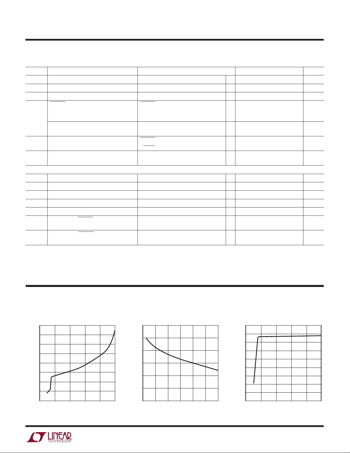
Supply Current vs Supply Voltage
1.8
1.7
1.6
1.5
1.4
1.3
SUPPLY CURRENT (mA)
1.2
1.1
0
20 40 80
0
SUPPLY VOLTAGE (V)
60
100
1640 G01
Supply Current vs Temperature
1.6
1.5
1.4
1.3
1.2
SUPPLY CURRENT (mA)
1.1
1.0
–50 –25
0255075
TEMPERATURE (°C)
1640 G02
100
unless otherwise
EE
Gate Voltage vs Supply Voltage
15
14
13
12
11
10
9
GATE VOLTAGE (V)
8
7
6
0
20 60
40
SUPPLY VOLTAGE (V)
80
100
1640 G03
1640lhfb
3
LT1640L/LT1640H
TEMPERATURE (°C)
–50
2
OUTPUT IMPEDANCE (kΩ)
3
4
5
6
7
8
–25 2505075
1640 G09
100
V
DRAIN
– VEE > 2.4V
UW
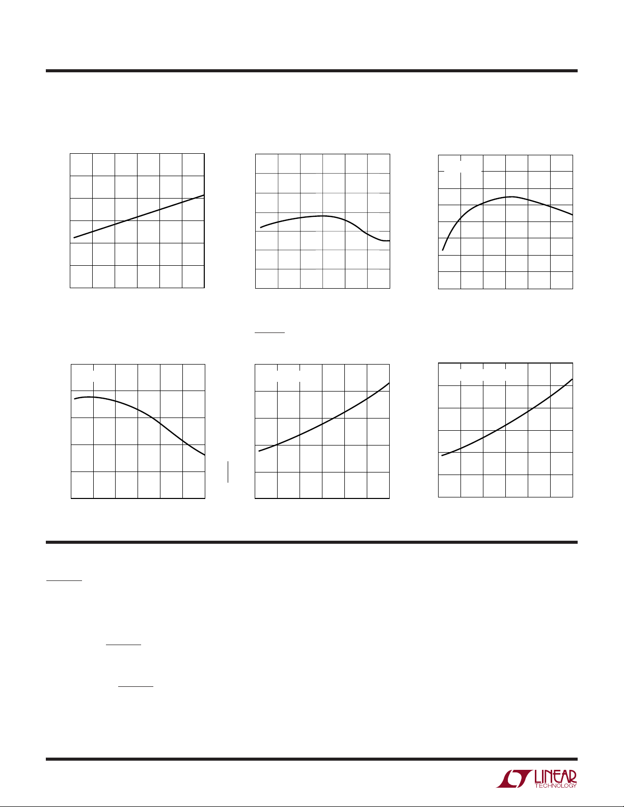
TYPICAL PERFOR A CE CHARACTERISTICS
Gate Voltage vs Temperature
15.0
14.5
14.0
13.5
13.0
GATE VOLTAGE (V)
12.5
12.0
–25 0 75
TEMPERATURE (°C)
Gate Pull-Down Current
vs Temperature
55
V
= 2V
GATE
52
49
1640 G04
Circuit Breaker Trip Voltage
vs Temperature
55
54
53
52
51
TRIP VOLTAGE (mV)
50
49
100–50 25 50
48
–50
–25
TEMPERATURE (°C)
50
250
100
75
1640 G05
PWRGD Output Low Voltage
vs Temperature (LT1640L)
0.5
I
= 1mA
OUT
0.4
0.3
Gate Pull-Up Current
vs Temperature
48
V
= 0V
GATE
47
46
45
44
43
42
GATE PULL-UP CURRENT (µA)
41
40
–25 10050250
–50
TEMPERATURE (°C)
PWRGD Output Impedance
vs Temperature (LT1640H)
75
1640 G06
46
43
GATE PULL-DOWN CURRENT (mA)
40
–25 0
–50
25
TEMPERATURE (°C)
50
75
100
1640 G07
0.2
0.1
PWRGD OUTPUT LOW VOLTAGE (V)
0
–25 25050
–50
TEMPERATURE (°C)
75
100
1640 G08
UUU
PIN FUNCTIONS
PWRGD/PWRGD (Pin 1): Power Good Output Pin. This pin
will toggle when V
is within VPG of VEE. This pin can
DRAIN
be connected directly to the enable pin of a power module.
When the DRAIN pin of the LT1640L is above VEE by more
than VPG, the PWRGD pin will be high impedance, allowing
the pull-up current of the module’s enable pin to pull the
pin high and turn the module off. When V
DRAIN
drops
below VPG, the PWRGD pin sinks current to VEE, pulling
the enable pin low and turning on the module.
When the DRAIN pin of the LT1640H is above VEE by more
than VPG, the PWRGD pin will sink current to the DRAIN
pin which pulls the module’s enable pin low, forcing it off.
When V
drops below VPG, the PWRGD sink current
DRAIN
is turned off and a 6.5k resistor is connected between
PWRGD and DRAIN, allowing the module’s pull-up current to pull the enable pin high and turn on the module.
OV (Pin 2): Analog Overvoltage Input. When OV is pulled
above the 1.223V low to high threshold, an overvoltage
condition is detected and the GATE pin will be immediately
pulled low. The GATE pin will remain low until OV drops
below the 1.203V high to low threshold.
1640lhfb
4

UUU
PIN FUNCTIONS
LT1640L/LT1640H
UV (Pin 3): Analog Undervoltage Input. When UV is
pulled below the 1.223V high to low threshold, an undervoltage condition is detected and the GATE pin will be
immediately pulled low. The GATE pin will remain low
until UV rises above the 1.243 low to high threshold.
The UV pin is also used to reset the electronic circuit
breaker. If the UV pin is cycled low and high following the
trip of the circuit breaker, the circuit breaker is reset and
a normal power-up sequence will occur.
VEE (Pin 4): Negative Supply Voltage Input. Connect to
the lower potential of the power supply.
SENSE (Pin 5): Circuit Breaker Sense Pin. With a sense
resistor placed in the supply path between VEE and
SENSE, the circuit breaker will trip when the voltage
across the resistor exceeds 50mV. Noise spikes of less
than 2µs are filtered out and will not trip the circuit
breaker.
If the circuit breaker trip current is set to twice the normal
operating current, only 25mV is dropped across the
sense resistor during normal operation. To disable the
circuit breaker, VEE and SENSE can be shorted together.
GATE (Pin 6): Gate Drive Output for the External
N-Channel. The GATE pin will go high when the following
start-up conditions are met: the UV pin is high, the OV pin
is low and (V
– VEE) < 50mV. The GATE pin is pulled
SENSE
high by a 45µA current source and pulled low with a
50mA current source.
DRAIN (Pin 7): Analog Drain Sense Input. Connect this
pin to the drain of the external N-channel and the V– pin
of the power module. When the DRAIN pin is below VPG,
the PWRGD or PWRGD pin will toggle.
VDD (Pin 8): Positive Supply Voltage Input. Connect this
pin to the higher potential of the power supply inputs and
the V+ pin of the power module. The input supply voltage
ranges from 10V to 80V.
BLOCK DIAGRA
UV
OV
–
+
REF
–
+
W
V
DD
V
REF
CC
OUTPUT
DRIVE
+
–
+
V
PG
–
V
EE
DRAIN
PWRGD/PWRGD
1640 BD
VCC AND
REFERENCE
GENERATOR
LOGIC
AND
50mV
EE
–
+
–
+
GATE DRIVE
GATESENSEV
1640lhfb
5

LT1640L/LT1640H
2V
1V
1640 F03
t
PHLUV
1.223V
0V
UV
GATE
1V
1.243V
t
PLHUV
1.8V
1V
1640 F05
0V
V
PWRGD
– V
DRAIN
= 0V
DRAIN
PWRGD
1V
1.4V
1.8V
1V
t
PLHPG
V
EE
V
EE
DRAIN
PWRGD
1V
1.4V
t
PHLPG
t
PLHPG
t
PHLPG
TEST CIRCUIT
WUW
TIMING DIAGRAMS
2V
OV
0V
1.223V
t
PHLOV
R
5k
+
V
5V
V
OV
V
UV
PWRGD/PWRGD V
OV
LT1640L/LT1640H
UV GATE
V
EE
DRAIN
SENSE
DD
V
DRAIN
V
SENSE
1640 F01
+
48V
–
Figure 1. Test Circuit
1.203V
t
PLHOV
GATE
SENSE
GATE
1V
Figure 2. OV to GATE Timing
50mV
t
PHLSENSE
1V
Figure 4. SENSE to GATE Timing
1V
1640 F02
Figure 3. UV to GATE Timing
1640 F04
Figure 5. DRAIN to PWRGD/PWRGD Timing
6
1640lhfb

LT1640L/LT1640H
U
WUU
APPLICATIONS INFORMATION
Hot Circuit Insertion
When circuit boards are inserted into a live – 48V backplane,
the bypass capacitors at the input of the board’s power
module or switching power supply can draw huge transient currents as they charge up. The transient currents
can cause permanent damage to the board’s components
and cause glitches on the system power supply.
The LT1640 is designed to turn on a board’s supply
voltage in a controlled manner, allowing the board to be
safely inserted or removed from a live backplane. The chip
also provides undervoltage, overvoltage and overcurrent
protection while keeping the power module off until its
input voltage is stable and within tolerance.
Power Supply Ramping
The input to the power module on a board is controlled by
placing an external N-channel pass transistor (Q1) in the
power path (Figure 6a, all waveforms are with respect to
the VEE pin of the LT1640). R1 provides current fault
detection and R2 prevents high frequency oscillations.
Resistors R4, R5 and R6 provide undervoltage and overvoltage sensing. By ramping the gate of Q1 up at a slow
rate, the surge current charging load capacitors C3 and C4
can be limited to a safe value when the board makes
connection.
Resistor R3 and capacitor C2 act as a feedback network to
accurately control the inrush current. The inrush current
can be calculated with the following equation:
I
INRUSH
= (45µA • CL)/C2
where CL is the total load capacitance, C3 + C4 + module
input capacitance.
(SHORT PIN)
GND
GND
R4
562k
UV = 37V
OV = 71V
–48V
* DIODES INC. SMAT70A
1%
R5
9.09k
1%
R6
10k
1%
*
8
V
3
UV
2
OV
V
EE
4
R1
0.02Ω
5%
SENSE
56
43
21
DD
LT1640H PWRGD
GATE DRAIN
2× 1N4148
Q1
IRF530
R2
10Ω
5%
R3
18k
5%
C2
3.3nF
100V
C1
150nF
25V
7
C3
0.1µF
100V
1
C4
+
100µF
100V
1640 F06a
VI-J3D-CY
+
V
IN
GATE IN
–
V
IN
VICOR
+
V
OUT
–
V
OUT
5V
+
C5
100µF
16V
Figure 6a. Inrush Control Circuitry
1640lhfb
7

LT1640L/LT1640H
U
WUU
APPLICATIONS INFORMATION
Capacitor C1 and resistor R3 prevent Q1 from momentarily turning on when the power pins first make contact.
Without C1 and R3, capacitor C2 would pull the gate of Q1
up to a voltage roughly equal to VEE • C2/CGS(Q1) before
the LT1640 could power up and actively pull the gate low.
By placing capacitor C1 in parallel with the gate capacitance of Q1 and isolating them from C2 using resistor R3
the problem is solved. The value of C1 should be:
VV
INMAX TH
V
TH
where VTH is the MOSFET’s minimum gate threshold and
V
is the maximum operating input voltage.
INMAX
−
2
CC
•+
()
GD
INRUSH
CURRENT
1A/DIV
R3’s value is not critical and is given by (V
INMAX
+ ∆V
GATE
)/
5mA.
The waveforms are shown in Figure 6b. When the power
pins make contact, they bounce several times. While the
contacts are bouncing, the LT1640 senses an undervoltage
condition and the GATE is immediately pulled low when
the power pins are disconnected.
Once the power pins stop bouncing, the GATE pin starts to
ramp up. When Q1 turns on, the GATE voltage is held
constant by the feedback network of R3 and C2. When the
DRAIN voltage has finished ramping, the GATE pin then
ramps to its final value.
GATE – V
10V/DIV
DRAIN
50V/DIV
50V/DIV
EE
V
EE
CONTACT
BOUNCE
5ms/DIV
Figure 6b. Inrush Control Waveforms
1640 F06b
8
1640lhfb

LT1640L/LT1640H
U
WUU
APPLICATIONS INFORMATION
Electronic Circuit Breaker
The LT1640 features an electronic circuit breaker function
that protects against short circuits or excessive supply
currents. By placing a sense resistor between the VEE and
SENSE pin, the circuit breaker will be tripped whenever the
voltage across the sense resistor is greater than 50mV for
more than 3µs as shown in Figure 7.
Note that the circuit breaker threshold should be set
sufficiently high to account for the sum of the load current
and the inrush current. If the load current can be controlled
by the PWRGD/PWRGD pin (as in Figure 6a), the threshold
can be set lower, since it will never need to accommodate
inrush current and load current simultaneously.
When the circuit breaker trips, the GATE pin is immediately
pulled to VEE and the external N-channel turns off. The
GATE pin will remain low until the circuit breaker is reset
by pulling UV low, then high or cycling power to the part.
If more than 3µs deglitching time is needed to reject
current noise, an external resistor and capacitor can be
added to the sense circuit as shown in Figure 8. R7 and C3
act as a lowpass filter that will slow down the SENSE pin
voltage from rising too fast. Since the SENSE pin will
source current, typically 20µA, there will be a voltage drop
on R7. This voltage will be counted into the circuit breaker
trip voltage just as the voltage across the sense resistor.
A small resistor is recommended for R7. A 100Ω for R7
will cause a 2mV error. The following equation can be used
to estimate the delay time at the SENSE pin:
–•• –
1
tRCIn
=
Vt Vt
()– ( )
VVt
–()
iO
O
Where V(t) is the circuit breaker trip voltage, typically
50mV. V(tO) is the voltage drop across the sense resistor
before the short or over current condition occurs. Vi is the
voltage across the sense resistor when the short current
or over current is applied on it.
Example: A system has a 1A current load and a 0.02Ω
sense resistor is used. An extended delay circuit needs to
be designed for a 50µs delay time after the load jumps to
5A. In this case:
V(t) = 50mV
V(tO) = 20mV
Vi = 5A • 0.02Ω = 100mV
If R7 = 100Ω, then C3 = 1µF.
INRUSH
CURRENT
2A/DIV
GATE – V
4V/DIV
50V/DIV
(SHORT PIN)
GND
GND
R4
562k
1%
3
1%
10k
1%
UV
R5
2
OV
R6
V
SENSE
EE
4
C3
R1
0.02Ω
5%
5
R7
43
21
UV = 37V
9.09k
EE
V
EE
4ms/DIV
1640 F07
OV = 71V
*
–48V
* DIODES INC. SMAT70A
8
V
DD
LT1640L
GATE DRAIN
6
R2
C1
10Ω
150nF
5%
25V
Q1
IRF530
1N4148
R3
18k
5%
C2
3.3nF
100V
PWRGD
1
+
C
L
100µF
100V
7
1640 F08
Figure 8. Extending the Short-Circuit Protection DelayFigure 7. Start-Up Into a Short Circuit
1640lhfb
9

LT1640L/LT1640H
U
WUU
APPLICATIONS INFORMATION
Under some conditions, a short circuit at the output can
cause the input supply to dip below the UV threshold,
resetting the circuit breaker immediately.
The LT1640 then cycles on and off repeatedly until the
short is removed. This can be minimized by adding a
deglitching delay to the UV pin with a capacitor from UV to
VEE. This capacitor forms an RC time constant with the
resistors at UV, allowing the input supply to recover before
the UV pin resets the circuit breaker.
A circuit that automatically resets the circuit breaker after
a current fault is shown in Figure 9.
(SHORT PIN)
GND
GND
R6
1%
10k
1%
R4
562k
1%
3
2
R5
R9
19.1k
1%
*
D1
1N4148
–48V
* DIODES INC. SMAT70A
2N2222
1µF
100V
Q2
R7
1M
5%
C4
3
ZVN3310
R8
510k
5%
562k
2
Q3
Transistors Q2 and Q3 along with R7, R8, C4 and D1 form
a programmable one-shot circuit. Before a short occurs,
the GATE pin is pulled high and Q3 is turned on, pulling
node 2 to VEE. Resistor R8 turns off Q2. When a short
occurs, the GATE pin is pulled low and Q3 turns off. Node
2 starts to charge C4 and Q2 turns on, pulling the UV pin
low and resetting the circuit breaker. As soon as C4 is fully
charged, R8 turns off Q2, UV goes high and the GATE
starts to ramp up. Q3 turns back on and quickly pulls node
2 back to VEE. Diode D1 clamps node 3 one diode drop
below VEE. The duty cycle is set to 10% to prevent Q1 from
overheating.
8
V
DD
UV
OV
LT1640L PWRGD
V
SENSE
EE
4
R1
0.02Ω
43
5%
21
GATE DRAIN
56
Q1
IRF530
R2
10Ω
5%
C1
150nF
25V
1N4148
R3
18k
5%
C2
3.3nF
100V
1
C3
+
100µF
100V
7
1640 F09a
10
NODE 2
50V/DIV
GATE
2V/DIV
1s/DIV
1640 F09b
Figure 9. Automatic Restart After Current Fault
1640lhfb

LT1640L/LT1640H
U
WUU
APPLICATIONS INFORMATION
Undervoltage and Overvoltage Detection
The UV (Pin 3) and OV (Pin 2) pins can be used to detect
undervoltage and overvoltage conditions at the power
supply input. The UV and OV pins are internally connected
to analog comparators with 20mV of hysteresis. When the
UV pin falls below its threshold or the OV pin rises above
its threshold, the GATE pin is immediately pulled low. The
GATE pin will be held low until UV is high and OV is low.
The undervoltage and overvoltage trip voltages can be
programmed using a three resistor divider as shown in
Figure 10a. With R4 = 562k, R5 = 9.09k and R6 = 10K, the
(SHORT PIN)
GND
GND
R4
VUV = 1.223
VOV = 1.223
R4 + R5+ R6
()
R5 + R6
R4 + R5+ R6
()
R5
R6
R6
–48V
undervoltage threshold is set to 37V and the overvoltage
threshold is set to 71V. The resistor divider will also gain
up the 20mV hysteresis at the UV pin and OV pin to 0.6V
and 1.2V at the input respectively.
More hysteresis can be added to the UV threshold by
connecting resistor R3 between the UV pin and the GATE
pin as shown in Figure 10b.
8
V
UV
OV
DD
LT1640L
LT1640H
V
EE
4
1640 F10a
3
2
Figure 10a. Undervoltage and Overvoltage Sensing
(SHORT PIN)
GND
GND
8
V
DD
2
OV
UV
V
EE
4
0.02Ω
LT1640L/LT1640H
SENSE
56
R1
43
5%
21
GATE
C1
150nF
25V
IRF530
R6
10Ω
5%
1640 F10b
Q1
3
506k
UV = 37.6V
UV = 43V
OV = 71V
8.87k
*
–48V
* DIODES INC. SMAT70A
1%
1%
R4
R1
562k
1%
R2
R5
16.9k
1%
R3
1.62M
1%
Figure 10b. Programmable Hysteresis for Undervoltage Detection
1640lhfb
11

LT1640L/LT1640H
U
WUU
APPLICATIONS INFORMATION
The new threshold voltage when the input moves from low
to high is:
R R RR RR
•••
++
VV
=
UV LH UVH,
where V
UVH
23 13 12
RR
•
23
is typically 1.243V.
The new threshold voltage when the input moves from
high to low is:
R R RR RR
•••
++
VV
UV HL UVL GATE,
where V
UVL
23 13 12
RR
•
23
is typically 1.223V.
The new hysteresis value will be:
VV
=
HYS UVHY GATE
R R RR RR
++
23 13 12
•••
RR
23
•
With R1 = 562k, R2 = 16.9k and R3 = 1.62M, V
and V
= 20mV, the undervoltage threshold will be 43V
UVHY
(from low to high) and 37.6V (from high to low). The
hysteresis is 5.4V. A separate resistor divider should be
used to set the overvoltage threshold given by:
V
–•=
V
+
GATE
R
1
R
3
R
1
•
R
3
= 13.5V
VV
=
OV OVH
RR
With R4 = 506k, R5 = 8.87k and V
+
45
R
5
= 1.223V, the
OVH
overvoltage threshold will be 71V.
PWRGD/PWRGD Output
The PWRGD/PWRGD output can be used to directly enable a power module when the input voltage to the module
is within tolerance. The LT1640L has a PWRGD output for
modules with an active low enable input, and the LT1640H
has a PWRGD output for modules with an active high
enable input.
When the DRAIN voltage of the LT1640H is high with
respect to VEE (Figure 11), the internal transistor Q3 is
turned off and R7 and Q2 clamp the PWRGD pin one diode
drop (≈0.7V) above the DRAIN pin. Transistor Q2 sinks
the module’s pull-up current and the module turns off.
When the DRAIN voltage drops below VPG, Q3 will turn on,
shorting the bottom of R7 to DRAIN and turning Q2 off.
The pull-up current in the module then flows through R7,
pulling the PWRGD pin high and enabling the module.
12
(SHORT PIN)
GND
GND
R4
3
R5
2
R6
*
–48V
* DIODES INC. SMAT70A
8
LT1640H
UV
+
–
OV
V
4
V
PG
SENSE
EE
R1
21
V
DD
+
–
56
C1
43
6.5k
R7
GATE
Q1
PWRGD
Q2
Q3
V
DRAIN
EE
R3
R2
Figure 11. Active High Enable Module
1
7
C2
2× 1N4148
+
1640 F11
ACTIVE HIGH
ENABLE MODULE
+
V
IN
ON/OFF
C3
–
V
IN
+
V
OUT
–
V
OUT
1640lhfb

LT1640L/LT1640H
U
WUU
APPLICATIONS INFORMATION
When the DRAIN voltage of the LT1640L is high with
respect to VEE, the internal pull-down transistor Q2 is off
and the PWRGD pin is in a high impedance state (Figure␣ 12). The PWRGD pin will be pulled high by the module’s
internal pull-up current source, turning the module off.
When the DRAIN voltage drops below VPG, Q2 will turn on
and the PWRGD pin will pull low, enabling the module.
The PWRGD signal can also be used to turn on an LED or
optoisolator to indicate that the power is good as shown
in Figure 13.
(SHORT PIN)
GND
GND
LT1640L
R4
3
UV
+
V
OV
PG
–
SENSE
V
EE
4
R5
2
R6
*
V
DD
+
–
GATE
56
C1
Gate Pin Voltage Regulation
When the supply voltage to the chip is more than 15.5V,
the GATE pin voltage is regulated at 13.5V above VEE. If the
supply voltage is less than 15.5V, the GATE voltage will be
about 2V below the supply voltage. At the minimum 10V
supply voltage, the gate voltage is guaranteed to be greater
than 6V. The gate voltage will be no greater than 18V for
supply voltages up to 80V.
ACTIVE LOW
ENABLE MODULE
+
+
V
V
OUT
8
PWRGD
R2
Q2
V
EE
DRAIN
R3
1
+
7
1N4148
C2
IN
ON/OFF
C3
–
–
V
V
OUT
IN
–48V
* DIODES INC. SMAT70A
(SHORT PIN)
GND
GND
R4
562k
1%
R5
9.09k
1%
R6
10k
1%
*
–48V
* DIODES INC. SMAT70A
43
R1
21
Q1
1640 F12
Figure 12. Active Low Enable Module
R7
51k
8
V
3
UV
2
OV
V
EE
4
SENSE
56
R1
0.02Ω
43
5%
21
DD
LT1640L PWRGD
GATE DRAIN
Q1
IRF530
R2
10Ω
5%
R3
18k
5%
C2
3.3nF
100V
C1
150nF
25V
7
1N4148
5%
+
MOC207
1
C3
100µF
100V
1640 F13
PWRGD
Figure 13. Using PWRGD to Drive an Optoisolator
1640lhfb
13
LT1640L/LT1640H
PACKAGE DESCRIPTION
U
N8 Package
8-Lead PDIP (Narrow .300 Inch)
(Reference LTC DWG # 05-08-1510)
0.255 ± 0.015*
(6.477 ± 0.381)
0.400*
(10.160)
MAX
876
5
12
0.300 – 0.325
(7.620 – 8.255)
0.065
(1.651)
0.009 – 0.015
(0.229 – 0.381)
+0.035
0.325
–0.015
+0.889
8.255
()
–0.381
*THESE DIMENSIONS DO NOT INCLUDE MOLD FLASH OR PROTRUSIONS.
MOLD FLASH OR PROTRUSIONS SHALL NOT EXCEED 0.010 INCH (0.254mm)
TYP
0.045 – 0.065
(1.143 – 1.651)
0.100
(2.54)
BSC
3
4
0.130 ± 0.005
(3.302 ± 0.127)
0.125
(3.175)
MIN
0.018 ± 0.003
(0.457 ± 0.076)
0.020
(0.508)
MIN
N8 1098
14
1640lhfb

PACKAGE DESCRIPTION
8-Lead Plastic Small Outline (Narrow .150 Inch)
U
S8 Package
(Reference LTC DWG # 05-08-1610)
0.189 – 0.197*
(4.801 – 5.004)
7
8
LT1640L/LT1640H
5
6
0.228 – 0.244
(5.791 – 6.197)
0.010 – 0.020
(0.254 – 0.508)
0.008 – 0.010
(0.203 – 0.254)
*
DIMENSION DOES NOT INCLUDE MOLD FLASH. MOLD FLASH
SHALL NOT EXCEED 0.006" (0.152mm) PER SIDE
**
DIMENSION DOES NOT INCLUDE INTERLEAD FLASH. INTERLEAD
FLASH SHALL NOT EXCEED 0.010" (0.254mm) PER SIDE
×
°
45
0.016 – 0.050
(0.406 – 1.270)
0°– 8° TYP
0.053 – 0.069
(1.346 – 1.752)
0.014 – 0.019
(0.355 – 0.483)
TYP
0.150 – 0.157**
(3.810 – 3.988)
1
3
2
4
0.004 – 0.010
(0.101 – 0.254)
0.050
(1.270)
BSC
SO8 1298
Information furnished by Linear Technology Corporation is believed to be accurate and reliable.
However, no responsibility is assumed for its use. Linear Technology Corporation makes no representation that the interconnection of its circuits as described herein will not infringe on existing patent rights.
1640lhfb
15

LT1640L/LT1640H
TYPICAL APPLICATION
U
Using an EMI Filter Module
Many applications place an EMI filter module in the power
path to prevent switching noise of the module from being
injected back onto the power supply. A typical application
(SHORT PIN)
GND
GND
R4
562k
1%
R5
9.09k
1%
R6
10k
1%
*
–48V
* DIODES INC. SMAT70A
8
V
DD
3
UV
LT1640L
2
OV
V
EE
4
R1
0.02Ω
5%
PWRGD
DRAIN
GATE
SENSE
21
1
1N4148
7
C2
3.3nF
100V
6
C1
5
150nF
25V
43
Q1
IRF530
R3
18k
5%
R2
10Ω
5%
1N4003
C3
0.1µF
100V
Figure 14. Typical Application Using a Filter Module
using the Lucent FLTR100V10 filter module is shown in
Figure 14. When using a filter, an optoisolator is required
to prevent common mode transients from destroying the
PWRGD and ON/OFF pins.
R7
51k
5%
MOC207
+
V
V
OUT
IN
LUCENT
FLTR100V10
–
V
V
OUT
IN
CASE
+
C4
0.1µF
100V
–
C5
+
100µF
100V
C6
0.1µF
100V
1
2
4
LUCENT
JW050A1-E
+
V
IN
ON/OFF
–
V
IN
CASE
V
OUT
SENSE
TRIM
SENSE
V
OUT
3
+
+
–
–
9
8
7
6
5
1640 F14
+
C7
100µF
16V
5V
RELATED PARTS
PART NUMBER DESCRIPTION COMMENTS
LTC®1421 Dual Channel, Hot Swap Controller Operates from 3V to 12V
LTC1422 High Side Drive, Hot Swap Controller in SO-8 System Reset Output with Programmable Delay
LT1640A –48V Hot Swap Controller in SO-8 LT1640 Pin Compatible, Improved Drain Pin Ruggedness
LT1641 48V Hot Swap Controller Foldback Analog Current Limit
LTC1642 Fault Protected Hot Swap Controller Operates Up to 16.5V, Protected to 33V
LTC1643 PCI Hot Swap Controller 3.3V, 5V, 12V, –12V Supplies for PCI Bus
LTC1645 Dual Hot Swap Controller Operates from 1.2V to 12V, Power Sequencing
LTC1646 CompactPCITM Hot Swap Controller 3.3V, 5V Supplies, 1V Precharge, Local PCI Reset Logic
LTC1647 Dual Hot Swap Controller Dual ON Pins for Supplies from 3V to 15V
LTC4211 Low Voltage Hot Swap Controller 2.5V to 16.5V, Dual Level Circuit Breaker, Active Inrush Limiting
LT4250 –48V Hot Swap Controller in SO-8 LT1640 Pin Compatible, Active Current Limiting
LTC4251 –48V Hot Swap Controller in SOT-23 Active Current Limiting, Fast Circuit Breaker for Short-Circuit Faults
CompactPCI is a trademark of the PCI Industrial Computer Manufacturers Group
1640lhfb
LT/TP 1101 1.5K REV B • PRINTED IN USA
LINEAR TECHNOLOGY CORPORATION 1998
16
Linear T echnolog y Corporation
1630 McCarthy Blvd., Milpitas, CA 95035-7417
(408) 432-1900 ● FAX: (408) 434-0507
●
www.linear.com
 Loading...